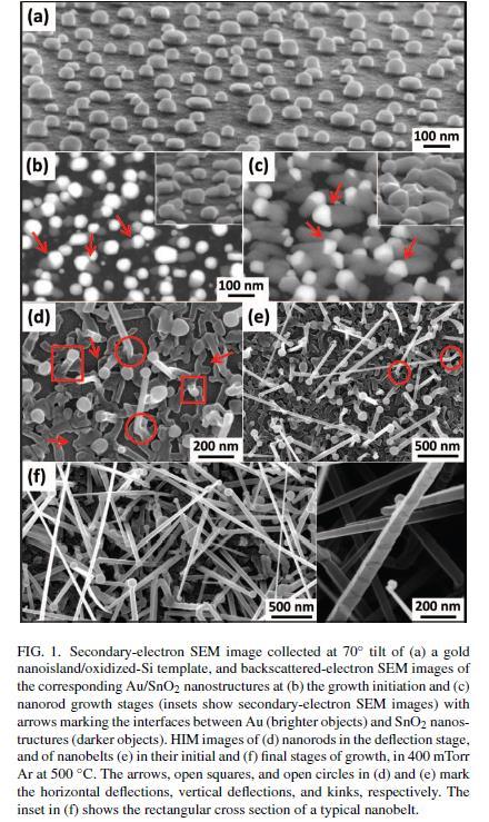
Electron
|
|
|
- Kory Simpson
- 5 years ago
- Views:
Transcription


")
1 Electron 1897: Sir Joseph John Thomson ( ) discovered corpuscles small particles with a charge-to-mass ratio over 1000 times greater than that of protons. Plum pudding model : electrons in a sea of positive charge. Nobel Prize : Sir George Paget Thomson ( ) discovered 10 kv electrons could give diffraction pattern of a 100 nm thick gold foil. Nobel Prize 1937, shared with Clinton Davison (experiment on Ni single crystal). 1924: Doctoral thesis of Louis-Victor Pierre Raymond de Broglie ( ) hypothesized matter waves and the idea of wave- particle duality (only known for photon up to then). Nobel Prize
2 Lecture 24 MNS 102: Techniques for Materials and Nano Sciences Reference: #1 C. R. Brundle, C. A. Evans, S. Wilson, "Encyclopedia of Materials Characterization", Butterworth-Heinemann, Toronto (1992), Ch. 2, Ch. 3. Reference: Electron Electron Microscopy Overview and History Comparison with Light Microscopy Transmission Electron Microscopy (TEM): Instrument and Electron Optics Comparison between TEM and LM Resolution, contributing factors to the resolution Depth of Focus and Depth of Field Modes of operation: Imaging vs Diffraction vs STEM Limitations of TEM 24-2
 can be used as lenses for electrons")
 began serious study of magnetic lenses potentially for EM")
3 History of Electron Microscopy 1926: Hans Busch ( ) demonstrated that electric and magnetic fields of axial symmetry (short magnetic coils) can be used as lenses for electrons and other charged particles father of electron optics? 1928: Ernst Ruska ( ) began serious study of magnetic lenses potentially for EM applications. PhD thesis in 1929 on magnetic lenses. 24-3
 with a 100 micron beam diameter.")
4 History of EM 1931: Max Knoll ( ) and Ruska realized the first but crude transmission electron microscope (TEM). 1932: Davisson and Calbrick studied electrostatic lenses. 1934: Driest and Muller showed EM surpassing LM in resolution. 1935: Knoll built the first scanning electron microscope (SEM) with a 100 micron beam diameter. 1938: Manfred von Ardenne built the first true SEM with a nm resolution. The machine was destroyed in the Berlin air raid in

, and for Scanning Tunnelling Microscopy (STM) to Gerd Binnig and Heinrich Rohrer.")
5 History of EM 1938: Albert Prebus, James Hillier of Professor Eli Franklin Burton s group at U of T Physics built the first TEM in North America. Their design was later adopted by all TEM manufacturers : 1 nm resolution achieved. 1961: First commercial SEM instruments after the invention of the secondary electron detector by Everhart and Thomley (ET). 1965: R.F. Pease and W. Nixon achieved 10 nm SEM resolution. 1986: Nobel Prize for Transmission Electron Microscopy to Ernst Ruska (TEM), and for Scanning Tunnelling Microscopy (STM) to Gerd Binnig and Heinrich Rohrer. 1997/98: Aberration correction 1999: Below 0.1 nm resolution achieved. 24-5

6 Everhart Thomley SE Detector SE = Secondary Electron 24-6


7 Example: Au (a = nm) 24-7

8 Transmission Electron Microscopy vs LM Specimen 24-8

 to select electrons for building the image, and to improve contrast of the")
9 TEM: Electron Optics 1 Double condenser lens: 1 st condenser to create demagnified image of the gun crossover and to minimize the spot size; 2 nd condenser to control beam divergence at the sample and the illumination spot size; condenser lens aperture to control illumination intensity. Objective lens: to form an inverted initial image that can subsequently be magnified, and to form a diffraction pattern in the back focal plane. Plus objective lens aperture (placed in the back focal plane of image) to select electrons for building the image, and to improve contrast of the final image. 24-9

10 TEM: Electron Optics 2 Intermediate lens: to magnify initial image formed by the objective lens, and to focus on initial image or diffraction pattern formed on the back focal plane. Projector lens: to magnify the size of image with various strengths

11 Electrostatic Lens vs Magnetic Lens Electrostatic lenses is used to focus electrons, e.g. in electron source to create a highly focussed e beam. Focussing is independent of the mass, i.e. electron and ions follow the same trajectory, and image is inverted like light optics. Paraxial ray approximation for converging lens. Magnetic lenses is used for condenser lenses and objective lenses Focussing is dependent of the charge-tomass ratio, i.e times less effective at focussing ions, and image is inverted and rotated. Focal length depends on the strength of the magnetic field
12 How sharp is the image? Contrast Conditions Contrast = (Max Signal Min Signal)/Max Signal Based on electron scattering theory quantum mechanics Inelastic scattering: occurs in all materials and leads to absorption Incoherent elastic scattering: particularly important for amorphous materials Coherent elastic scattering: leads to diffraction from single crystal regions 24-12
13 Light Microscopy vs Electron Microscopy Light Microscope Electron Microscope Wavelength = 500 nm (150/V 0 ) = nm at 50 kv Refraction Index = n 1.5 (glass) 1.0 (vacuum) Half-angle = 70 deg 1 deg Resolution = 0.61 / NA where NA = n sin Depth of Focus (DOF) = distance parallel to the optical axis that a feature on the specimen can be displaced without loss of resolution. 200 nm 0.16 nm* DOF = λ n2 NA NA 2 M 2 M = 10, DOF = 60 m M = 100, DOF = 8 m M = 1,000, DOF = 200 nm 0.1 mm DOF = M θ M = 10, DOF = 1,000 m M = 100, DOF = 100 m M = 1,000, DOF = 10 m M = 10,000, DOF = 1 m *Less than 0.05 nm possible with Cs (spherical aberration) and Cc (chromatic aberration) lens correctors. Most TEM specimens are not thin enough to produce images with resolution that could benefit from Cs correction. For thicker specimens, Cc correction via energy filtering is much more useful
14 Resolution Diffraction Limit Diffraction limit gives: Nonrelativistic electron wavelength vs relativistic electron wavelength 24-14
15 Resolution Homework 6A: Calculate the nonrelativistic wavelength, relativistic wavelength, relativistic mass, and speed for an 1, 10, 20, and 80 kev electron. Relativistic mass is the rest mass (m 0 ) multiplied by the highlighted term. For electron, m 0 is 9.1x10⁻³¹ Kg
 Diffraction effects: For = 0.0037 nm (for a 100 kev electron beam), and C S = 1 mm (for TEM objective lens), d min = 0.474 nm. 24-16")
16 Aberration and Diffraction Effects Spherical aberration: For a good magnetic lens design, K S ~ 1 and for an electrostatic lens, K S > 1, must be very small (~ 0.01 rad). Chromatic aberration: d = C C ( E/E) Diffraction effects: For = nm (for a 100 kev electron beam), and C S = 1 mm (for TEM objective lens), d min = nm
17 Resolution: EM vs LM With higher kv (300 kv to 500 kv) and proper C S correction, resolution of 0.05 nm may be realized
18 24-18
19 Light Microscopy vs Electron Microscopy Light Microscope Electron Microscope Wavelength = 500 nm (150/V 0 ) = nm at 50 kv Refraction Index = n 1.5 (glass) 1.0 (vacuum) Half-angle = 70 deg 1 deg Resolution = 0.61 / NA where NA = n sin Depth of Focus (DOF) = distance parallel to the optical axis that a feature on the specimen can be displaced without loss of resolution. 200 nm 0.16 nm* DOF = λ n2 NA NA 2 M 2 M = 10, DOF = 60 m M = 100, DOF = 8 m M = 1,000, DOF = 200 nm 0.1 mm DOF = M θ M = 10, DOF = 1,000 m M = 100, DOF = 100 m M = 1,000, DOF = 10 m M = 10,000, DOF = 1 m *Less than 0.05 nm possible with Cs (spherical aberration) and Cc (chromatic aberration) lens correctors. Most TEM specimens are not thin enough to produce images with resolution that could benefit from Cs correction. For thicker specimens, Cc correction via energy filtering is much more useful


20 DOF Depth of field corresponds to how much of the 3D object remains in focus at the same time. Depth of focus corresponds to the distance over which the image can move relative to the object and still remain in focus
21 Modes of Operation: Imaging vs Diffraction Usually, we do a low resolution imaging scan to get a quick survey image, then we proceed to obtain a high-resolution image (HRTEM) to resolve the fringes. The fringe spacings (between planes of columns of atoms) will tell us directly the interplanar separation between specific planes. We can also obtain a diffraction pattern of a selected area (called SAED = Selected Area Electron Diffraction). Just like XRD (except for the extremely small sampling area), these ED patterns contain detailed info about the crystallography. The third mode is the STEM mode
. Diffraction pattern and image are simultaneously present in the TEM.")
22 Imaging vs Diffraction An objective lens is used to form a diffraction pattern in the back focal plane with electrons scattered by the sample and combine them to generate an image in the image plane (1. intermediate image). Diffraction pattern and image are simultaneously present in the TEM. By controlling the strength of the intermediate lens, they can be made to appear in the plane of the second intermediate image and magnified by the projective lens on the viewing screen. In imaging mode, an objective aperture can be inserted in the back focal plane to select one or more beams that contribute to the final image (BF, DF, HRTEM). For selected area electron diffraction (SAED), an aperture in the plane of the first intermediate image defines the region of which the diffraction is obtained


23 Bright Field vs Dark Field Imaging BF: An aperture is placed in the back focal plane of the objective lens which allows only the direct beam to pass. Image results from a weakening of the direct beam by its interaction with the sample. Therefore, mass-thickness and diffraction contrast contribute to image formation: thick areas, areas in which heavy atoms are enriched, and crystalline areas appear with dark contrast. DF: The direct beam is blocked by the aperture while one or more diffracted beams are allowed to pass the objective aperture. Since diffracted beams have strongly interacted with the specimen, very useful information is present in DF images, e.g., about planar defects, stacking faults or particle size
, some crystals appear with dark contrast since they are")

, some of the microcrystals appear with bright contrast, namely")
24 BF vs DF TEM BF and DF images of the same area of microcrystalline ZrO 2. In the BF image (centre), some crystals appear with dark contrast since they are oriented (almost) parallel to a zone axis (Bragg contrast). Thickness contrast also occurs: areas close to the edge are thinner and thus appear brighter (lower right side) than those far of the edge (upper left side). In the DF image (right), some of the microcrystals appear with bright contrast, namely such whose diffracted beams partly pass the objective aperture
.")
 images are obtained. In many cases, the atomic structure of a specimen can directly be investigated by HRTEM.")
25 High-Resolution TEM Imaging HRTEM: A large objective aperture has to be selected that allows many beams including the direct beam to pass. The image is formed by the interference of the diffracted beams with the direct beam (phase contrast). If the point resolution of the microscope is sufficiently high and a suitable crystalline sample oriented along a zone axis, then high-resolution TEM (HRTEM) images are obtained. In many cases, the atomic structure of a specimen can directly be investigated by HRTEM. This corresponds to columns of atoms along the zone axis
26 24-26
 detectors. Undiffracted beam is detected by the Bright Field (BF) detector.")
, orientation")
27 TEM vs STEM (Scanning TEM) Specimen STEM mode: The electron beam is rastered across the specimen and the transmitted electrons are detected by various (annular) detectors. Undiffracted beam is detected by the Bright Field (BF) detector. Diffracted beams are detected either by the Annular Dark Field (ADF) detector or High Angle ADF (HAADF) detector. Signals from BF, ADF, HAADF can be used to provide info about material type (composition and structure), orientation (diffraction) and topography


28 FePt Alloy Nanoparticles for Biosensing: Enhancement of Vitamin C Sensor Performance and Selectivity by Nanoalloying Nafiseh Moghimi, K.T. Leung* WATLab, and Department of Chemistry University of Waterloo Waterloo, Ontario, Canada N2L3G
29 Limitations of TEM Sampling: The higher the resolution, the smaller the amount of materials that the TEM examines. The total amount of materials sampled by TEM in the past 15 years is no more than 0.3 mm 3 very tiny! 2D projection of a 3D specimen: The image contains columns of atoms from the top surface, middle section, and the bottom surface. Not really true 2D and definitely not 3D Tomography is being developed to overcome this problem but this requires large specimen rotation (> 120 deg) to get full 3D info. Electron beam damage: The energy of the e-beam is large enough to displace atoms in the specimen. Most materials (organic, biological, polymer, many ceramics) will suffer radiation damage above 80 kev. Specimen preparation: The quality of the info obtained greatly depends on how and how good the specimen is prepared. Specimen thickness should be less than 100 nm generally, but the thinner the specimen the better the quality of the image. Methods include slicing, fracturing, ion milling, electrochemical polishing, focussed ion beam (FIB) preparation 24-29

30 WATLab TEM: Zeiss Libra 200MC for-materials.html 24-30
Chapter 2 Instrumentation for Analytical Electron Microscopy Lecture 7. Chapter 2 CHEM Fall L. Ma
 Chapter 2 Instrumentation for Analytical Electron Microscopy Lecture 7 Outline Electron Sources (Electron Guns) Thermionic: LaB 6 or W Field emission gun: cold or Schottky Lenses Focusing Aberration Probe
Introduction to Electron Microscopy
 Introduction to Electron Microscopy Prof. David Muller, dm24@cornell.edu Rm 274 Clark Hall, 255-4065 Ernst Ruska and Max Knoll built the first electron microscope in 1931 (Nobel Prize to Ruska in 1986)
NANO 703-Notes. Chapter 9-The Instrument
 1 Chapter 9-The Instrument Illumination (condenser) system Before (above) the sample, the purpose of electron lenses is to form the beam/probe that will illuminate the sample. Our electron source is macroscopic
Chapter 1. Basic Electron Optics (Lecture 2)
") Chapter 1. Basic Electron Optics (Lecture 2) Basic concepts of microscope (Cont ) Fundamental properties of electrons Electron Scattering Instrumentation Basic conceptions of microscope (Cont ) Ray diagram
Chapter 1. Basic Electron Optics (Lecture 2) Basic concepts of microscope (Cont ) Fundamental properties of electrons Electron Scattering Instrumentation Basic conceptions of microscope (Cont ) Ray diagram
Chapter 4 Imaging Lecture 17
 Chapter 4 Imaging Lecture 17 d (110) Imaging Imaging in the TEM Diffraction Contrast in TEM Image HRTEM (High Resolution Transmission Electron Microscopy) Imaging STEM imaging Imaging in the TEM What is
NanoSpective, Inc Progress Drive Suite 137 Orlando, Florida
 TEM Techniques Summary The TEM is an analytical instrument in which a thin membrane (typically < 100nm) is placed in the path of an energetic and highly coherent beam of electrons. Typical operating voltages
Transmission electron Microscopy
 Transmission electron Microscopy Image formation of a concave lens in geometrical optics Some basic features of the transmission electron microscope (TEM) can be understood from by analogy with the operation
Transmission Electron Microscopy 9. The Instrument. Outline
 Transmission Electron Microscopy 9. The Instrument EMA 6518 Spring 2009 02/25/09 Outline The Illumination System The Objective Lens and Stage Forming Diffraction Patterns and Images Alignment and Stigmation
ELECTRON MICROSCOPY. 13:10 16:00, Oct. 6, 2008 Institute of Physics, Academia Sinica. Tung Hsu
 ELECTRON MICROSCOPY 13:10 16:00, Oct. 6, 2008 Institute of Physics, Academia Sinica Tung Hsu Department of Materials Science and Engineering National Tsing Hua University Hsinchu 300, TAIWAN Tel. 03-5742564
ELECTRON MICROSCOPY. 14:10 17:00, Apr. 3, 2007 Department of Physics, National Taiwan University. Tung Hsu
 ELECTRON MICROSCOPY 14:10 17:00, Apr. 3, 2007 Department of Physics, National Taiwan University Tung Hsu Department of Materials Science and Engineering National Tsinghua University Hsinchu 300, TAIWAN
Transmissions Electron Microscopy (TEM)
") Transmissions Electron Microscopy (TEM) Basic principles Diffraction Imaging Specimen preparation A.E. Gunnæs MENA3100 V17 TEM is based on three possible set of techniqes Diffraction From regions down
Transmissions Electron Microscopy (TEM) Basic principles Diffraction Imaging Specimen preparation A.E. Gunnæs MENA3100 V17 TEM is based on three possible set of techniqes Diffraction From regions down
Nanotechnology in Consumer Products
 Nanotechnology in Consumer Products Advances in Transmission Electron Microscopy Friday, April 21, 2017 October 31, 2014 The webinar will begin at 1pm Eastern Time Click here to watch the webinar recording
Introduction to Transmission Electron Microscopy (Physical Sciences)
") Introduction to Transmission Electron Microscopy (Physical Sciences) Centre for Advanced Microscopy Program 9:30 10:45 Lecture 1 Basics of TEM 10:45 11:00 Morning tea 11:00 12:15 Lecture 2 Diffraction
Introduction to Transmission Electron Microscopy (Physical Sciences) Centre for Advanced Microscopy Program 9:30 10:45 Lecture 1 Basics of TEM 10:45 11:00 Morning tea 11:00 12:15 Lecture 2 Diffraction
VISUAL PHYSICS ONLINE DEPTH STUDY: ELECTRON MICROSCOPES
 VISUAL PHYSICS ONLINE DEPTH STUDY: ELECTRON MICROSCOPES Shortly after the experimental confirmation of the wave properties of the electron, it was suggested that the electron could be used to examine objects
Introduction of New Products
 Field Emission Electron Microscope JEM-3100F For evaluation of materials in the fields of nanoscience and nanomaterials science, TEM is required to provide resolution and analytical capabilities that can
Lecture 23 MNS 102: Techniques for Materials and Nano Sciences
 Lecture 23 MNS 102: Techniques for Materials and Nano Sciences Reference: #1 C. R. Brundle, C. A. Evans, S. Wilson, "Encyclopedia of Materials Characterization", Butterworth-Heinemann, Toronto (1992),
Low Voltage Electron Microscope
 LVEM5 Low Voltage Electron Microscope Nanoscale from your benchtop LVEM5 Delong America DELONG INSTRUMENTS COMPACT BUT POWERFUL The LVEM5 is designed to excel across a broad range of applications in material
Cs-corrector. Felix de Haas
 Cs-corrector. Felix de Haas Content Non corrector systems Lens aberrations and how to minimize? Corrector systems How is it done? Lens aberrations Spherical aberration Astigmatism Coma Chromatic Quality
ELECTRON MICROSCOPY AN OVERVIEW
 ELECTRON MICROSCOPY AN OVERVIEW Anjali Priya 1, Abhishek Singh 2, Nikhil Anand Srivastava 3 1,2,3 Department of Electrical & Instrumentation, Sant Longowal Institute of Engg. & Technology, Sangrur, India.
MODULE I SCANNING ELECTRON MICROSCOPE (SEM)
") MODULE I SCANNING ELECTRON MICROSCOPE (SEM) Scanning Electron Microscope (SEM) Initially, the plan of SEM was offered by H. Stintzing in 1927 (a German patent application). His suggested procedure was
MODULE I SCANNING ELECTRON MICROSCOPE (SEM) Scanning Electron Microscope (SEM) Initially, the plan of SEM was offered by H. Stintzing in 1927 (a German patent application). His suggested procedure was
2.Components of an electron microscope. a) vacuum systems, b) electron guns, c) electron optics, d) detectors. Marco Cantoni 021/
 vacuum systems, b) electron guns, c) electron optics, d) detectors. Marco Cantoni 021/") 2.Components of an electron microscope a) vacuum systems, b) electron guns, c) electron optics, d) detectors, 021/693.48.16 Centre Interdisciplinaire de Microscopie Electronique CIME Summary Electron propagation
2.Components of an electron microscope a) vacuum systems, b) electron guns, c) electron optics, d) detectors, 021/693.48.16 Centre Interdisciplinaire de Microscopie Electronique CIME Summary Electron propagation
Nanotechnology and material science Lecture V
 Most widely used nanoscale microscopy. Based on possibility to create bright electron beam with sub-nm spot size. History: Ernst Ruska (1931), Nobel Prize (1986) For visible light λ=400-700nm, for electrons
Low-energy Electron Diffractive Imaging for Three dimensional Light-element Materials
 Low-energy Electron Diffractive Imaging for Three dimensional Light-element Materials Hitachi Review Vol. 61 (2012), No. 6 269 Osamu Kamimura, Ph. D. Takashi Dobashi OVERVIEW: Hitachi has been developing
Introduction to Electron Microscopy-II
 Introduction to Electron Microscopy-II Prof. David Muller, dm24@cornell.edu Rm 274 Clark Hall, 255-4065 Ernst Ruska and Max Knoll built the first electron microscope in 1931 (Nobel Prize to Ruska in 1986)
Low Voltage Electron Microscope. Nanoscale from your benchtop LVEM5. Delong America
 LVEM5 Low Voltage Electron Microscope Nanoscale from your benchtop LVEM5 Delong America DELONG INSTRUMENTS COMPACT BUT POWERFUL The LVEM5 is designed to excel across a broad range of applications in material
2.Components of an electron microscope. a) vacuum systems, b) electron guns, c) electron optics, d) detectors. Marco Cantoni, 021/
 vacuum systems, b) electron guns, c) electron optics, d) detectors. Marco Cantoni, 021/") 2.Components of an electron microscope a) vacuum systems, b) electron guns, c) electron optics, d) detectors Marco Cantoni, 021/693.48.16 Centre Interdisciplinaire de Microscopie Electronique CIME MSE-603
2.Components of an electron microscope a) vacuum systems, b) electron guns, c) electron optics, d) detectors Marco Cantoni, 021/693.48.16 Centre Interdisciplinaire de Microscopie Electronique CIME MSE-603
S200 Course LECTURE 1 TEM
 S200 Course LECTURE 1 TEM Development of Electron Microscopy 1897 Discovery of the electron (J.J. Thompson) 1924 Particle and wave theory (L. de Broglie) 1926 Electromagnetic Lens (H. Busch) 1932 Construction
Scanning electron microscope
 Scanning electron microscope 6 th CEMM workshop Maja Koblar, Sc. Eng. Physics Outline The basic principle? What is an electron? Parts of the SEM Electron gun Electromagnetic lenses Apertures Chamber and
ELECTRON MICROSCOPY. 09:10 12:00, Oct. 27, 2006 Institute of Physics, Academia Sinica. Tung Hsu
 ELECTRON MICROSCOPY 09:10 12:00, Oct. 27, 2006 Institute of Physics, Academia Sinica Tung Hsu Department of Materials Science and Engineering National Tsinghua University Hsinchu 300, TAIWAN Tel. 03-5742564
Chapter Ray and Wave Optics
 109 Chapter Ray and Wave Optics 1. An astronomical telescope has a large aperture to [2002] reduce spherical aberration have high resolution increase span of observation have low dispersion. 2. If two
CHAPTER TWO METALLOGRAPHY & MICROSCOPY
 CHAPTER TWO METALLOGRAPHY & MICROSCOPY 1. INTRODUCTION: Materials characterisation has two main aspects: Accurately measuring the physical, mechanical and chemical properties of materials Accurately measuring
Low Voltage Electron Microscope
 LVEM 25 Low Voltage Electron Microscope fast compact powerful Delong America FAST, COMPACT AND POWERFUL The LVEM 25 offers a high-contrast, high-throughput, and compact solution with nanometer resolutions.
LVEM 25. Low Voltage Electron Mictoscope. fast compact powerful
 LVEM 25 Low Voltage Electron Mictoscope fast compact powerful FAST, COMPACT AND POWERFUL The LVEM 25 offers a high-contrast, high-throughput, and compact solution with nanometer resolutions. All the benefits
High Resolution Transmission Electron Microscopy (HRTEM) Summary 4/11/2018. Thomas LaGrange Faculty Lecturer and Senior Staff Scientist
 Summary 4/11/2018. Thomas LaGrange Faculty Lecturer and Senior Staff Scientist") Thomas LaGrange Faculty Lecturer and Senior Staff Scientist High Resolution Transmission Electron Microscopy (HRTEM) Doctoral Course MS-637 April 16-18th, 2018 Summary Contrast in TEM images results from
Thomas LaGrange Faculty Lecturer and Senior Staff Scientist High Resolution Transmission Electron Microscopy (HRTEM) Doctoral Course MS-637 April 16-18th, 2018 Summary Contrast in TEM images results from
Scanning electron microscope
 Scanning electron microscope 5 th CEMM workshop Maja Koblar, Sc. Eng. Physics Outline The basic principle? What is an electron? Parts of the SEM Electron gun Electromagnetic lenses Apertures Detectors
The Resolution in the Electron Microscopy
 Volume 3, Issue, February 1 ISSN 319-87 The Resolution in the Electron Microscopy ABSTRACT Benefit from the group's equations, especially the resolution limits in the transmission electron microscope (TEM)
Introduction to Light Microscopy. (Image: T. Wittman, Scripps)
") Introduction to Light Microscopy (Image: T. Wittman, Scripps) The Light Microscope Four centuries of history Vibrant current development One of the most widely used research tools A. Khodjakov et al. Major
Introduction to Light Microscopy (Image: T. Wittman, Scripps) The Light Microscope Four centuries of history Vibrant current development One of the most widely used research tools A. Khodjakov et al. Major
Applied Optics. , Physics Department (Room #36-401) , ,
 , ,") Applied Optics Professor, Physics Department (Room #36-401) 2290-0923, 019-539-0923, shsong@hanyang.ac.kr Office Hours Mondays 15:00-16:30, Wednesdays 15:00-16:30 TA (Ph.D. student, Room #36-415) 2290-0921,
Applied Optics Professor, Physics Department (Room #36-401) 2290-0923, 019-539-0923, shsong@hanyang.ac.kr Office Hours Mondays 15:00-16:30, Wednesdays 15:00-16:30 TA (Ph.D. student, Room #36-415) 2290-0921,
(Refer Slide Time: 00:10)
") Fundamentals of optical and scanning electron microscopy Dr. S. Sankaran Department of Metallurgical and Materials Engineering Indian Institute of Technology, Madras Module 03 Unit-6 Instrumental details
Fundamentals of optical and scanning electron microscopy Dr. S. Sankaran Department of Metallurgical and Materials Engineering Indian Institute of Technology, Madras Module 03 Unit-6 Instrumental details
Microscopy. ( greek mikros = small; skopein = to observe)
") Microscopy ( greek mikros = small; skopein = to observe) Zacharias Jansen put several lenses in a tube (first compound microscope) and the object near the end of tube appeared to be greatly enlarged, much
Microscopy ( greek mikros = small; skopein = to observe) Zacharias Jansen put several lenses in a tube (first compound microscope) and the object near the end of tube appeared to be greatly enlarged, much
Electron Sources, Optics and Detectors
 Thomas LaGrange, Ph.D. Faculty Lecturer and Senior Staff Scientist Electron Sources, Optics and Detectors TEM Doctoral Course MS-637 April 16 th -18 th, 2018 Summary Electron propagation is only possible
TEM theory Basic optics, image formation and key elements
 Workshop series of Chinese 3DEM community Get acquainted with Cryo-Electron Microscopy: First Chinese Workshop for Structural Biologists TEM theory Basic optics, image formation and key elements Jianlin
INTRODUCTION THIN LENSES. Introduction. given by the paraxial refraction equation derived last lecture: Thin lenses (19.1) = 1. Double-lens systems
 = 1. Double-lens systems") Chapter 9 OPTICAL INSTRUMENTS Introduction Thin lenses Double-lens systems Aberrations Camera Human eye Compound microscope Summary INTRODUCTION Knowledge of geometrical optics, diffraction and interference,
Chapter 9 OPTICAL INSTRUMENTS Introduction Thin lenses Double-lens systems Aberrations Camera Human eye Compound microscope Summary INTRODUCTION Knowledge of geometrical optics, diffraction and interference,
The Wave Nature of Light
 The Wave Nature of Light Physics 102 Lecture 7 4 April 2002 Pick up Grating & Foil & Pin 4 Apr 2002 Physics 102 Lecture 7 1 Light acts like a wave! Last week we saw that light travels from place to place
Scanning Electron Microscopy. EMSE-515 F. Ernst
 Scanning Electron Microscopy EMSE-515 F. Ernst 1 2 Scanning Electron Microscopy Max Knoll Manfred von Ardenne Manfred von Ardenne Principle of Scanning Electron Microscopy 3 Principle of Scanning Electron
Lecture 20: Optical Tools for MEMS Imaging
 MECH 466 Microelectromechanical Systems University of Victoria Dept. of Mechanical Engineering Lecture 20: Optical Tools for MEMS Imaging 1 Overview Optical Microscopes Video Microscopes Scanning Electron
ABC Math Student Copy. N. May ABC Math Student Copy. Physics Week 13(Sem. 2) Name. Light Chapter Summary Cont d 2
 Name. Light Chapter Summary Cont d 2") Page 1 of 12 Physics Week 13(Sem. 2) Name Light Chapter Summary Cont d 2 Lens Abberation Lenses can have two types of abberation, spherical and chromic. Abberation occurs when the rays forming an image
Page 1 of 12 Physics Week 13(Sem. 2) Name Light Chapter Summary Cont d 2 Lens Abberation Lenses can have two types of abberation, spherical and chromic. Abberation occurs when the rays forming an image
Confocal Imaging Through Scattering Media with a Volume Holographic Filter
 Confocal Imaging Through Scattering Media with a Volume Holographic Filter Michal Balberg +, George Barbastathis*, Sergio Fantini % and David J. Brady University of Illinois at Urbana-Champaign, Urbana,
No part of this material may be reproduced without explicit written permission.
 This material is provided for educational use only. The information in these slides including all data, images and related materials are the property of : Robert M. Glaeser Department of Molecular & Cell
Topics 3b,c Electron Microscopy
 Topics 3b,c Electron Microscopy 1.0 Introduction and History 1.1 Characteristic Information 2.0 Basic Principles 2.1 Electron-Solid Interactions 2.2 Electromagnetic Lenses 2.3 Breakdown of an Electron
Fabrication of Probes for High Resolution Optical Microscopy
 Fabrication of Probes for High Resolution Optical Microscopy Physics 564 Applied Optics Professor Andrès La Rosa David Logan May 27, 2010 Abstract Near Field Scanning Optical Microscopy (NSOM) is a technique
microscopy A great online resource Molecular Expressions, a Microscope Primer Partha Roy
 Fundamentals of optical microscopy A great online resource Molecular Expressions, a Microscope Primer http://micro.magnet.fsu.edu/primer/index.html Partha Roy 1 Why microscopy Topics Functions of a microscope
The Compound Microscope. Brightfield: Köhler Illumination
 Outline History of Microscopy The Magnifying Glass The Compound Microscope Brightfield: Köhler Illumination Microscopy µικροσ (mikros): small σκοπειν (skopein): to observe History of Microscopy Well :
Introduction to Scanning Electron Microscopy
 Introduction to Scanning Electron Microscopy By: Brandon Cheney Ant s Leg Integrated Circuit Nano-composite This document was created as part of a Senior Project in the Materials Engineering Department
A few concepts in TEM and STEM explained
 A few concepts in TEM and STEM explained Martin Ek November 23, 2011 1 Introduction This is a collection of short, qualitative explanations of key concepts in TEM and STEM. Most of them are beyond what
Reflection! Reflection and Virtual Image!
 1/30/14 Reflection - wave hits non-absorptive surface surface of a smooth water pool - incident vs. reflected wave law of reflection - concept for all electromagnetic waves - wave theory: reflected back
Observing Microorganisms through a Microscope LIGHT MICROSCOPY: This type of microscope uses visible light to observe specimens. Compound Light Micros
 PHARMACEUTICAL MICROBIOLOGY JIGAR SHAH INSTITUTE OF PHARMACY NIRMA UNIVERSITY Observing Microorganisms through a Microscope LIGHT MICROSCOPY: This type of microscope uses visible light to observe specimens.
Resolution. Diffraction from apertures limits resolution. Rayleigh criterion θ Rayleigh = 1.22 λ/d 1 peak at 2 nd minimum. θ f D
 Microscopy Outline 1. Resolution and Simple Optical Microscope 2. Contrast enhancement: Dark field, Fluorescence (Chelsea & Peter), Phase Contrast, DIC 3. Newer Methods: Scanning Tunneling microscopy (STM),
Microscope anatomy, image formation and resolution
 Microscope anatomy, image formation and resolution Ian Dobbie Buy this book for your lab: D.B. Murphy, "Fundamentals of light microscopy and electronic imaging", ISBN 0-471-25391-X Visit these websites:
--> Buy True-PDF --> Auto-delivered in 0~10 minutes. JY/T
 Translated English of Chinese Standard: JY/T011-1996 www.chinesestandard.net Sales@ChineseStandard.net INDUSTRY STANDARD OF THE JY PEOPLE S REPUBLIC OF CHINA General rules for transmission electron microscopy
Functions of the SEM subsystems
 Functions of the SEM subsystems Electronic column It consists of an electron gun and two or more electron lenses, which influence the path of electrons traveling down an evacuated tube. The base of the
OPAC 202 Optical Design and Instrumentation. Topic 3 Review Of Geometrical and Wave Optics. Department of
 OPAC 202 Optical Design and Instrumentation Topic 3 Review Of Geometrical and Wave Optics Department of http://www.gantep.edu.tr/~bingul/opac202 Optical & Acustical Engineering Gaziantep University Feb
Microscopy Techniques that make it easy to see things this small.
 Microscopy Techniques that make it easy to see things this small. What is a Microscope? An instrument for viewing objects that are too small to be seen easily by the naked eye. Dutch spectacle-makers Hans
Point Spread Function. Confocal Laser Scanning Microscopy. Confocal Aperture. Optical aberrations. Alternative Scanning Microscopy
 Bi177 Lecture 5 Adding the Third Dimension Wide-field Imaging Point Spread Function Deconvolution Confocal Laser Scanning Microscopy Confocal Aperture Optical aberrations Alternative Scanning Microscopy
Oct. 30th- Nov. 1st, 2017
 Thomas LaGrange, Ph.D. Faculty Lecturer and Senior Staff Scientist Electron Sources, Optics and Detectors SEM Doctoral Course MS-636 Oct. 30th- Nov. 1st, 2017 Summary Electron propagation is only possible
Introduction: Why electrons?
 Introduction: Why electrons? 1 Radiations Visible light X-rays Electrons Neutrons Advantages Not very damaging Easily focused Eye wonderful detector Small wavelength (Angstroms) Good penetration Small
EE119 Introduction to Optical Engineering Spring 2003 Final Exam. Name:
 EE119 Introduction to Optical Engineering Spring 2003 Final Exam Name: SID: CLOSED BOOK. THREE 8 1/2 X 11 SHEETS OF NOTES, AND SCIENTIFIC POCKET CALCULATOR PERMITTED. TIME ALLOTTED: 180 MINUTES Fundamental
Full-screen mode Popup controls. Overview of the microscope user interface, TEM User Interface and TIA on the left and EDS on the right
 Quick Guide to Operating FEI Titan Themis G2 200 (S)TEM: TEM mode Susheng Tan Nanoscale Fabrication and Characterization Facility, University of Pittsburgh Office: M104/B01 Benedum Hall, 412-383-5978,
OPTICAL PRINCIPLES OF MICROSCOPY. Interuniversity Course 28 December 2003 Aryeh M. Weiss Bar Ilan University
 OPTICAL PRINCIPLES OF MICROSCOPY Interuniversity Course 28 December 2003 Aryeh M. Weiss Bar Ilan University FOREWORD This slide set was originally presented at the ISM Workshop on Theoretical and Experimental
GBS765 Hybrid methods
 GBS765 Hybrid methods Lecture 3 Contrast and image formation 10/20/14 4:37 PM The lens ray diagram Magnification M = A/a = v/u and 1/u + 1/v = 1/f where f is the focal length The lens ray diagram So we
Chapter 25. Optical Instruments
 Chapter 25 Optical Instruments Optical Instruments Analysis generally involves the laws of reflection and refraction Analysis uses the procedures of geometric optics To explain certain phenomena, the wave
PHYSICS. Chapter 35 Lecture FOR SCIENTISTS AND ENGINEERS A STRATEGIC APPROACH 4/E RANDALL D. KNIGHT
 PHYSICS FOR SCIENTISTS AND ENGINEERS A STRATEGIC APPROACH 4/E Chapter 35 Lecture RANDALL D. KNIGHT Chapter 35 Optical Instruments IN THIS CHAPTER, you will learn about some common optical instruments and
CS-TEM vs CS-STEM. FEI Titan CIME EPFL. Duncan Alexander EPFL-CIME
 CS-TEM vs CS-STEM Duncan Alexander EPFL-CIME 1 FEI Titan Themis @ CIME EPFL 60 300 kv Monochromator High brightness X-FEG Probe Cs-corrected: 0.7 Å @ 300 kv Image Cs-corrected: 0.7 Å @ 300 kv Super-X EDX
Scanning Electron Microscopy Basics and Applications
 Scanning Electron Microscopy Basics and Applications Dr. Julia Deuschle Stuttgart Center for Electron Microscopy MPI for Solid State Research Room: 1E15, phone: 0711/ 689-1193 email: j.deuschle@fkf.mpg.de
Optical Components for Laser Applications. Günter Toesko - Laserseminar BLZ im Dezember
 Günter Toesko - Laserseminar BLZ im Dezember 2009 1 Aberrations An optical aberration is a distortion in the image formed by an optical system compared to the original. It can arise for a number of reasons
EE119 Introduction to Optical Engineering Fall 2009 Final Exam. Name:
 EE119 Introduction to Optical Engineering Fall 2009 Final Exam Name: SID: CLOSED BOOK. THREE 8 1/2 X 11 SHEETS OF NOTES, AND SCIENTIFIC POCKET CALCULATOR PERMITTED. TIME ALLOTTED: 180 MINUTES Fundamental
Chapter 1. Introduction
 Chapter 1 Introduction 1.1 Where are the Atoms? Uncovering objects that are too small to be seen by eye: this is the primary purpose of microscopy. The human eye enables us to resolve objects that are
FYS 4340/FYS Diffraction Methods & Electron Microscopy. Lecture 9. Imaging Part I. Sandeep Gorantla. FYS 4340/9340 course Autumn
 FYS 4340/FYS 9340 Diffraction Methods & Electron Microscopy Lecture 9 Imaging Part I Sandeep Gorantla FYS 4340/9340 course Autumn 2016 1 Imaging 2 Abbe s principle of imaging Unlike with visible light,
Name. Light Chapter Summary Cont d. Refraction
 Page 1 of 17 Physics Week 12(Sem. 2) Name Light Chapter Summary Cont d with a smaller index of refraction to a material with a larger index of refraction, the light refracts towards the normal line. Also,
Oct. 30th- Nov. 1st, 2017
 Thomas LaGrange, Ph.D. Faculty Lecturer and Senior Staff Scientist Electron Sources, Optics and Detectors SEM Doctoral Course MS-636 Oct. 30th- Nov. 1st, 2017 Summary Electron propagation is only possible
The Nature of Light. Light and Energy
 The Nature of Light Light and Energy - dependent on energy from the sun, directly and indirectly - solar energy intimately associated with existence of life -light absorption: dissipate as heat emitted
Mirrors and Lenses. Images can be formed by reflection from mirrors. Images can be formed by refraction through lenses.
 Mirrors and Lenses Images can be formed by reflection from mirrors. Images can be formed by refraction through lenses. Notation for Mirrors and Lenses The object distance is the distance from the object
TSBB09 Image Sensors 2018-HT2. Image Formation Part 1
 TSBB09 Image Sensors 2018-HT2 Image Formation Part 1 Basic physics Electromagnetic radiation consists of electromagnetic waves With energy That propagate through space The waves consist of transversal
Microscopy: Fundamental Principles and Practical Approaches
 Microscopy: Fundamental Principles and Practical Approaches Simon Atkinson Online Resource: http://micro.magnet.fsu.edu/primer/index.html Book: Murphy, D.B. Fundamentals of Light Microscopy and Electronic
CCAM Microscope Objectives
 CCAM Microscope Objectives Things to consider when selecting an objective Magnification Numerical Aperture (NA) resolving power and light intensity of the objective Working Distance distance between the
Microscopy techniques for biomaterials. Engenharia Biomédica. Patrícia Almeida Carvalho
 Microscopy techniques for biomaterials Engenharia Biomédica Patrícia Almeida Carvalho 1 2 Why microscopy? http://www.cellsalive.com/howbig.htm 3 Why microscopy? Resolution of an optical system Diffraction
Scanning Electron Microscopy
 Scanning Electron Microscopy For the semiconductor industry A tutorial Titel Vorname Nachname Titel Jobtitle, Bereich/Abteilung Overview Scanning Electron microscopy Scanning Electron Microscopy (SEM)
Lecture 21. Physics 1202: Lecture 21 Today s Agenda
 Physics 1202: Lecture 21 Today s Agenda Announcements: Team problems today Team 14: Gregory Desautels, Benjamin Hallisey, Kyle Mcginnis Team 15: Austin Dion, Nicholas Gandza, Paul Macgillis-Falcon Homework
attocfm I for Surface Quality Inspection NANOSCOPY APPLICATION NOTE M01 RELATED PRODUCTS G
 APPLICATION NOTE M01 attocfm I for Surface Quality Inspection Confocal microscopes work by scanning a tiny light spot on a sample and by measuring the scattered light in the illuminated volume. First,
Chapter 2 The Study of Microbial Structure: Microscopy and Specimen Preparation
 Chapter 2 The Study of Microbial Structure: Microscopy and Specimen Preparation 1 Lenses and the Bending of Light light is refracted (bent) when passing from one medium to another refractive index a measure
Observing Microorganisms through a Microscope
 2016/2/19 PowerPoint Lecture Presentations prepared by Bradley W. Christian, McLennan Community College CHAPTER 3 Observing Microorganisms through a Microscope 1 Figure 3.2 Microscopes and Magnification.
High-resolution imaging on C s -corrected Titan
 High-resolution imaging on C s -corrected Titan 80-300 A new era for new results In NanoResearch a detailed knowledge of the structure of the material down to the atomic level is crucial for understanding
CS-TEM vs CS-STEM. FEI Titan CIME EPFL. Duncan Alexander EPFL-CIME
 CS-TEM vs CS-STEM Duncan Alexander EPFL-CIME 1 FEI Titan Themis @ CIME EPFL 60 300 kv Monochromator High brightness X-FEG Probe Cs-corrected: 0.7 Å @ 300 kv Image Cs-corrected: 0.7 Å @ 300 kv Super-X EDX
Applications of Optics
 Nicholas J. Giordano www.cengage.com/physics/giordano Chapter 26 Applications of Optics Marilyn Akins, PhD Broome Community College Applications of Optics Many devices are based on the principles of optics
Numerical analysis to verifying the performance of condenser magnetic lens in the scanning electron microscope.
 Numerical analysis to verifying the performance of condenser magnetic lens in the scanning electron microscope. Mohammed Abdullah Hussein Dept. of mechanization and agricultural equipment, College of agriculture
Lithography. 3 rd. lecture: introduction. Prof. Yosi Shacham-Diamand. Fall 2004
 Lithography 3 rd lecture: introduction Prof. Yosi Shacham-Diamand Fall 2004 1 List of content Fundamental principles Characteristics parameters Exposure systems 2 Fundamental principles Aerial Image Exposure
Atomic Resolution Imaging with a sub-50 pm Electron Probe
 Atomic Resolution Imaging with a sub-50 pm Electron Probe Rolf Erni, Marta D. Rossell, Christian Kisielowski, Ulrich Dahmen National Center for Electron Microscopy, Lawrence Berkeley National Laboratory
Lens Design I Seminar 5
 Y. Sekman, X. Lu, H. Gross Friedrich Schiller University Jena Institute of Applied Physics Albert-Einstein-Str 15 07745 Jena Lens Design I Seminar 5 Exercise 5-1: PSF scaling (Homework) To check the Airy
Converging and Diverging Surfaces. Lenses. Converging Surface
 Lenses Sandy Skoglund 2 Converging and Diverging s AIR Converging If the surface is convex, it is a converging surface in the sense that the parallel rays bend toward each other after passing through the
A Tutorial on Electron Microscopy
 A Tutorial on Electron Microscopy Jian-Min (Jim) Zuo Mat. Sci. Eng. and Seitz-Materials Research Lab., UIUC Outline of This Tutorial I. Science and opportunities of electron microscopy II. The basic TEM,