Microscopy techniques for biomaterials. Engenharia Biomédica. Patrícia Almeida Carvalho
|
|
|
- Rafe O’Connor’
- 6 years ago
- Views:
Transcription

1 Microscopy techniques for biomaterials Engenharia Biomédica Patrícia Almeida Carvalho 1


2 2 Why microscopy?
3 3 Why microscopy?

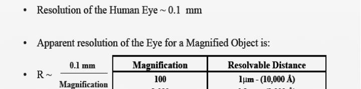
4 Resolution of an optical system Diffraction at an aperture - Rayleigh criterion The Rayleigh criterion for the resolution of an optical system states that two points will be resolvable if the maximum of the intensity of the Airy ring from one of them coincides with the first minimum intensity of the Airy ring of the other. This implies that the resolution, ρ (strictly resolving power) is given by: ρ = 0.6λ/η /ηsinα where λ is the wavelength, η the refractive index and α is the semi-angle at the specimen. 4
 are not deflected. 3. Parallel rays diverge from and converge to the focal points. 4.")
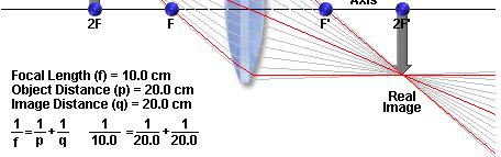
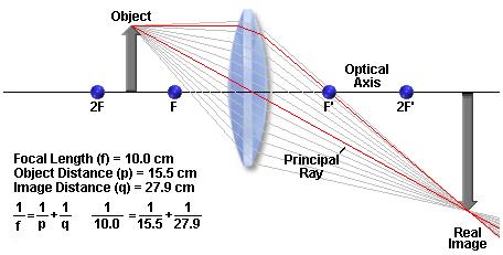
5 Introduction to lenses Ray diagrams (geometrical optics): 1. The optical axis contains the object focal point and the image focal point. 2. Rays going through the lens optical center (principal rays) are not deflected. 3. Parallel rays diverge from and converge to the focal points. 4. For identical optical media on both sides: f object = f image 1/a + 1/b = 1/f M = b/a 5

6 Image Formation 6

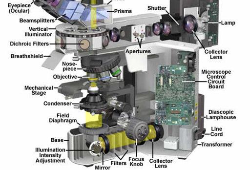
7 Compound Microscope 7

")

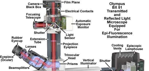
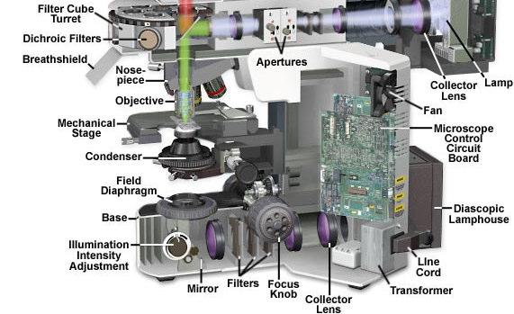
8 Compound Microscope Transmission (Diascopic) Transmission (Diascopic)
9 Compound Microscope Transmission (Diascopic) Reflection (Episcopic)
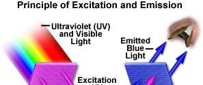
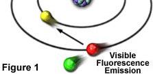
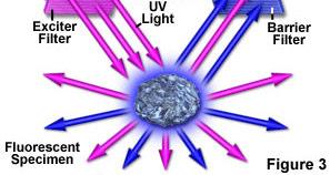
10 Fluorescence Microscopy 10
11 Fluorescence Microscopy 11
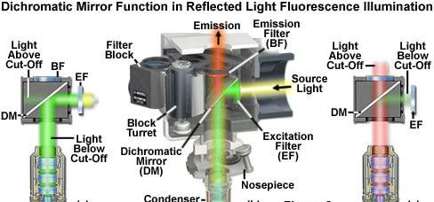
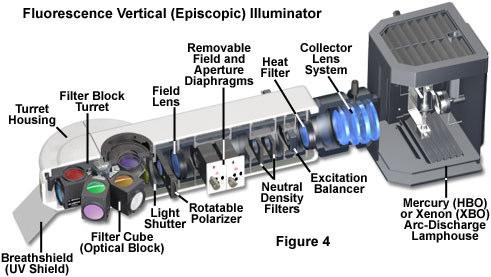
12 Fluorescence Microscopy 12


13 Confocal microscopy The Instrument (Laser Scanning confocal microscope) Confocal or conjugate planes ρ = 0.6λ/ηsinα ρ = 0.41λ/ηsinα Reflection mode: surface topography 13

.")

14 Confocal microscopy Samples are stained with fluorochromes that stain specific phases or organelles (labeling). Corresponding images are collected in the red, green, and blue channels and recombined. 14


15 Confocal microscopy 15

16 Confocal microscopy Tomography 16
17 17 Microscope working principles

18 Image Types JEOL images 18
19 Light vs electrons ρ = 0.61λ/ηsinα 19
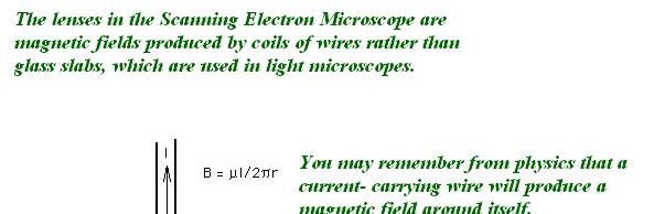
20 20 Electromagnetic Lenses
21 21 Electromagnetic Lenses
22 22 Electromagnetic Lenses
23 23 Electromagnetic Lenses
24 24 Electromagnetic Lenses
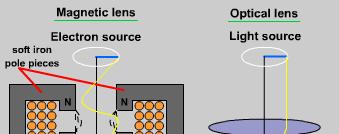
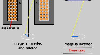
25 Electromagnetic Lenses Electromagnetic lenses 25


26 Scanning Electron Microscopy working principles 26

27 Scanning Electron Microscopy The Microscope Hitachi S 2400


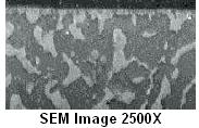
28 Scanning Electron Microscopy Depth of field - Light vs electrons (JEOL) Optical Microscope Image SEM Image of Same Object 28

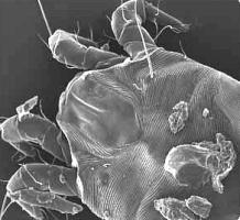
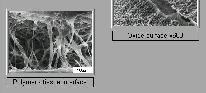
29 Scanning Electron Microscopy Woven polyester-fiber cloth House dust mite
30 Scanning Electron Microscopy The instrument Electron gun Gun alignment coils Condenser lens Secondary electron detector Deflection coils Objective lens Backscatter electron detector Specimen goniometer stage Oil diffusion vacuum pump Specimen chamber 30


31 Scanning Electron Microscopy Tungsten Hairpin Filament LaB 6 Pointed Rod Electron Gun - Cathodes Tungsten field-emission cathode 31


32 Scanning Electron Microscopy Electron Gun - Thermionic vs Field Emission 32
33 Scanning Electron Microscopy The condenser lens, often composed of a series of condensers, is primarily responsible for the production of the small probe diameter. With the demagnification of the probe, there is an unavoidable loss in current from the probe. Condenser and Objective (lenses) The purpose of the objective lens is to obtain the smallest diameter beam at the surface of the sample. It achieves this operating in the very same manner as the condenser lens. However, it received the name "objective" in analogy to the focusing done by the objective lens in the light microscope. 33
34 Scanning Electron Microscopy Scanning Coils Deflection Coils The scanning coils serve many functions, all related to the placement of the electron beam on the sample: -raster scanning, coupled to the image CRT. This is the mechanism for image formation and magnification. -fine positioning of the raster on the sample, by applying a DC voltage to the coils (electronic imageshift). -selected area electron channeling patterns, by rocking the beam about a point on the specimen. -x-ray analysis of a single feature or spot, by shutting off the rastering and using the scanning coils to position the beam on the sample. 34

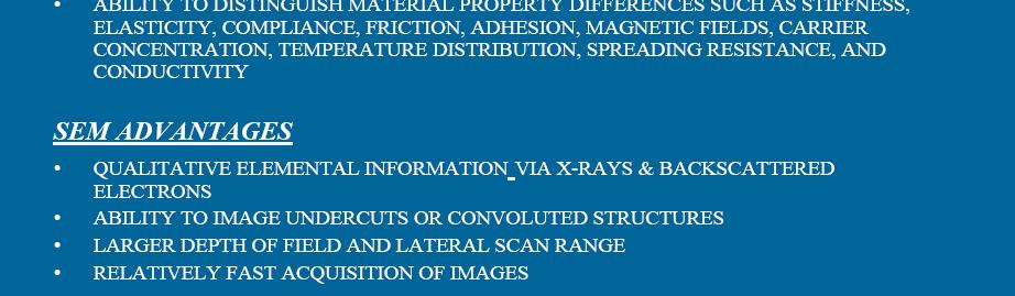
35 Scanning Electron Microscopy Beam-specimen interactions (signal types) 35

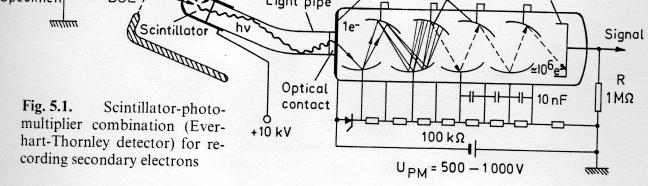
36 Scanning Electron Microscopy Everhart-Thornley Electron Detector 36
 The effect of surface topography on the escape of secondary electrons from within the")
37 Scanning Electron Microscopy Topographic contrast (where do the shades come from?) The effect of surface topography on the escape of secondary electrons from within the sample 37
38 Scanning Electron Microscopy Backscattered electron detector 38
39 Scanning Electron Microscopy Secondary vs Backscattered electron images (JEOL) Topographic contrast (SE mode) Atomic number contrast (BSE mode) 39


40 Scanning Electron Microscopy BSE images 40
41 41 Energy Dispersive Spectroscopy


42 Energy Dispersive Spectroscopy Background Deconvolution Corrections ZAF Z atomic number A Absorption F Fluorescence 42
43 Energy Dispersive Spectroscopy Analyses Types Qualitative Semi-quantitative (standardless) Quantitative Semi-quantitative (standardless) Element Atomic % Weight % Al Si Ti Cr Mn Fe Ni Nb Mo
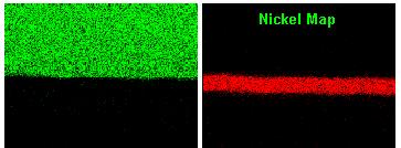
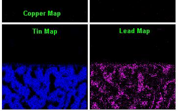
44 Energy Dispersive Spectroscopy X-Ray maps 44
45 Advantages vs Disadvantages of SEM Advantages - high depth of field - direct observation of the external form of real objects at high magnifications - wide range of magnifications (below 50 x to over x) Disadvantages of SEM - high vacuum environment of the specimen (porous, biological samples ) - inability to show internal detail - inability to obtain highest resolution - conductive layer 45
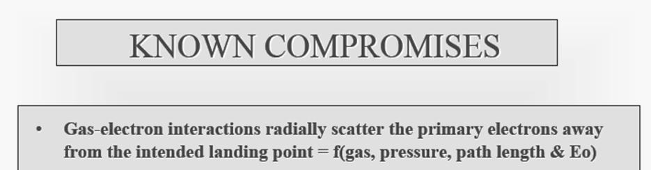
46 Environmental SEM Beam-Gas Interactions 46


47 Environmental SEM Environmental Secondary Detector The environmental Secondary Detector uses gas ionization to amplify the secondary electron signal. In non-conductive samples, positive ions are attracted to the sample surface where negative charges from the beam tend to accumulate. The positive ions effectively suppress charge artifacts!!! What are the implications for ceramic, polymer and biological samples observation? 47
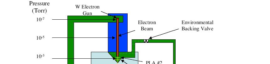
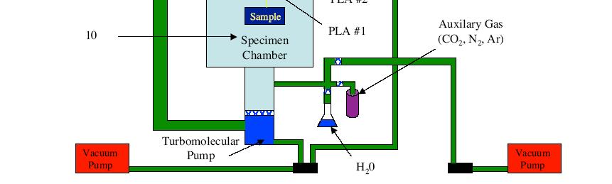
48 Environmental SEM PLA Pressure Limiting Aperture 48
49 49 Environmental SEM
50 Transmission electron microscopy TEM is an analytical tool that allows detailed investigation of the morphology, structure, and local chemistry of metals, ceramics, polymers, biological materials and minerals. It also enables the investigation of crystal structures, crystallographic orientations through electron diffraction, as well as second phase, precipitates and contaminants distribution by x-ray and electron-energy analysis. Magnifications of up to 500,000x and detail resolution below 1 nm are achieved routinely. Quantitative and qualitative elemental analysis can be provided from features smaller than 30 nm. For crystals with interplanar spacing greater than 0.12 nm, crystal structure, symmetry and orientation can be determined. Structural identification of defects, including stacking faults and dislocations is possible. 50


51 Transmission electron microscopy The Instrument A TEM usually operates at 10-6 Torr in the column and 10-7 Torr in the electron gun chamber. These are the important parts of a TEM and their general interaction. 51


.")
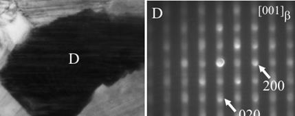
52 Transmission electron microscopy Ray Diagram The optical system of the TEM: The objective lens simultaneously generates the diffraction pattern and the first intermediate image. Note that the ray paths are identical until the intermediate lens, where the field strengths are changed, depending on the desired operation mode. The field strengths can be changed by setting the focal lengths (the distance from the lens to the ray crossover). A higher field strength (shorter focal length) is used for imaging, whereas a weaker field strength (longer focal length) is used for diffraction. 52

53 Transmission electron microscopy What results from a higher field strength for a fixed final image plane? 53
54 Transmission electron microscopy Imaging Techniques Bright field Bright-field imaging is used for examination of most microstructural imaging. In order to examine samples in bright-field, the objective aperture must be inserted. The objective aperture is a metal plate with holes of various sizes machined into it. The aperture is inserted into the back focal plane, the same plane at which the diffraction pattern is formed. The back focal plane is located just below the sample and objective lens. When the aperture is inserted, it only allows the electrons in the transmitted beam to pass and contribute to the resulting bright-field image. 54
55 Transmission electron microscopy Imaging Techniques Dark field Dark-field images occur when the objective aperture is positioned off-axis from the transmitted beam in order to allow only a diffracted beam to pass. In order to minimize the effects of lens aberrations, the diffracted beam is deflected along the optic axis 55
56 Transmission electron microscopy Bright Field Images When an electron beam strikes a sample, some of the electrons pass directly through while others may undergo slight inelastic scattering from the transmitted beam. Contrast in an image is created by differences in scattering. By inserting an aperture in the back focal plane, an image can be produced with these transmitted electrons. The resulting image is known as a bright field image. Bright field images are commonly used to examine micro-structural related features. BF image of a twinned crystal in strong contrast. Crystalline defects shown in a BF image 56


57 Transmission electron microscopy Dark Field Images If a sample is crystalline, many of the electrons will undergo elastic scattering from the various (hkl) planes. This scattering produces many diffracted beams. If any of these diffracted beams is allowed to pass through the objective aperture a dark field image is obtained. In order to reduce spherical aberration and astigmatism and to improve overall image resolution, the diffracted beam will be deflected such that it lies parallel the optic axis of the microscope. This type of image is said to be a centered dark field image. Dark field images are particularly useful in examining micro-structural detail in a single crystalline phases. DF image of a twinned crystal in strong contrast. Crystalline defects shown in a DF image 57


 Stained")
58 Transmission electron microscopy Bright Field Images (J.S.J. Vastenhout, Microsc Microanal 8 Suppl. 2, 2002) Stained with OsO 4 and RuO 4 vapors 58
")
 - (cellular")


59 Transmission electron microscopy (more examples) acrylonitril-butadiene-styrene copolymer (ABS) - (cellular rubber particles) (LEICA) Schierholz JU, Hellmann GP. In situ graft copolymerization: salami morphologies in PMMA/EP blends: part I. Polymer 2003;44:
 Copolymer stained with iodine")

60 Transmission electron microscopy (more examples) Copolymer stained with iodine vapor. The insert shows the FFT of the image (Akora, Briber, Kofinas, Polymer 47 (2006) 2018) 60


61 Transmission electron microscopy High-Resolution An atomic resolution image is formed by the "phase contrast" technique, which exploits the differences in phase among the various electron beams scattered by the sample in order to produce contrast. A large objective lens aperture allows the transmitted beam and at least four diffracted beams to form an image. 61


62 Transmission electron microscopy (more examples) HRETM 62


63 Transmission electron microscopy Electron tomography Imaging technique combines many images taken from different perspectives to create a three dimensional model of the sample. Data collection involves collecting images while tilting the specimen around a single axis. Software is used to combine the images into a 3-D representation. Nephrin at a porous slit diaphragm (Sidec Technologies ) 100 nm 5 nm 63

64 Transmission electron microscopy Diffraction Techniques Spot Patterns (Selected area diffraction SAD) are created when electrons are diffracted in a single crystal region of a given specimen. The center spot corresponds to the transmitted electron beam. Other spots are diffracted portions of the initial electron beam. Spot Patterns can be used for unknown phase identification and identification of crystal structure and orientation. The location of the spots are again governed by Bragg's law. SAD is a technique to reduce both the area and intensity of the beam contributing to a diffraction pattern by the insertion of an aperture into the image plane of the objective lens. This produces a virtual diaphragm in the plane of the specimen. Diffraction pattern from a single crystal of silicon in the <111> orientation. 64
 atomic planes. Two cones of diffracted electrons are created by each set of (hkl) planes.")
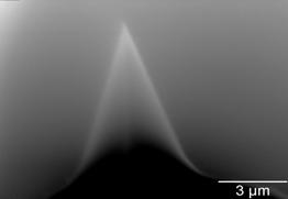
65 Transmission electron microscopy Diffraction Techniques Kikuchi Patterns created when a selected area diffraction pattern is taken from a thick region of the thin foil. Some electrons will be elastically scattered by Bragg diffraction from the various (hkl) atomic planes. Two cones of diffracted electrons are created by each set of (hkl) planes. The Kikuchi lines are actually arcs of intersection from these large radii diffraction cones. One cone will be more intense than the general background and produce a bright line. This is the excess line. The second cone will be less intense and produce a dark line (see arrows). This is the deficit line. Kikuchi Patterns allow for very accurate determination of crystal orientation and are an important factor in establishing the proper diffracting conditions for generating high-contrast images. Kikuchi Pattern from a thick sample of silicon. The six-fold symmetrical distribution in this pattern is a good indicator that the sample is very close to the <111> orientation. 65

66 Transmission electron microscopy Diffraction Techniques Convergent-Beam Electron Diffraction CBED Patterns allow examination of diffraction patterns from specimen volumes less than 0.5 mm in diameter. In order to generate a diffraction pattern from such a small area, an electron beam must be focused. The resulting diffraction pattern will be a series of disks rather than sharp spots due to highly convergent electron probe. The diameter of these disks is then proportional to the beam convergence angle. CBED patterns are routinely used to do crystallographic analysis of small volumes, such as fine precipitates in thin foil specimens. CBED pattern taken from a stainless steel single crystal viewing along the [111] zone axis. 66
67 Transmission electron microscopy Diffraction Techniques Ring Patterns created when electron diffraction occurs simultaneously from many grains with different orientations relative to the incident electron beam. Analogous to x-ray powder diffraction, ring patterns, can be used to identify unknown phases or characterize the crystallography of a material. The radii and spacing of the rings are governed by: Rd = λl where d is the interplanar spacing, R is the ring radius, and L is known as the camera constant. Ring diffraction patterns from polycrystalline gold indexed to show which atomic planes (hkl) are contributing to the ring. 67

68 Transmission electron microscopy Structural and chemical diversity of sialoliths Calcification Hydroxyapatite 500 nm


69 Transmission electron microscopy Structural and chemical diversity of sialoliths Calcification 100 nm 250 nm [0001] - [1010] Hydroxyapatite
70 Transmission electron microscopy (more examples) Bright-Field TEM 70

71 Transmission electron microscopy (more examples) Ring Diffraction patterns Crystalline with planar defects Partially amorphous 71


72 Transmission electron microscopy (more examples) Structure identification?? Simulations 72
73 Transmission electron microscopy (more examples) Structure identification Simulations?? 73
74 Transmission electron microscopy Sample Requisites Specimens for examination by TEM must meet the following requirements: Thin enough for electrons to penetrate without excessive energy loss. Be representative of the structure and composition. For penetration of a 200 kv electron beam, a typical metal, ceramic, or semiconductor specimen must be less than 100 nm thick. However, the specimen is required to represent the unaltered bulk material in terms of structure, chemistry, and content of defects. If one also wishes this specimen to have large amounts of electrontransparent thin area, be flat and unbent, and be strong enough to be easily handled, the task of making such a specimen from an arbitrary material is very difficult. Some specimens such as thin films may be examined directly with very little specimen preparation. 74
75 Transmission electron microscopy Sample Requisites Specimens for examination by TEM must meet the following requirements: Thin enough for electrons to penetrate without excessive energy loss. Be representative of the structure and composition. For penetration of a 200 kv electron beam, a typical metal, ceramic, or semiconductor specimen must be less than 100 nm thick. However, the specimen is required to represent the unaltered bulk material in terms of structure, chemistry, and content of defects. If one also wishes this specimen to have large amounts of electrontransparent thin area, be flat and unbent, and be strong enough to be easily handled, the task of making such a specimen from an arbitrary material is very difficult. Some specimens such as thin films may be examined directly with very little specimen preparation. 75


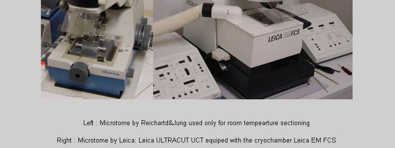
76 Transmission electron microscopy Sample Preparation Bulk/Interfaces - ceramics or metals Powder Samples prepared by suspension in a liquid. The suspension is dropped onto a mounting grid disperses the powder across it. The solvent, which is unreactive with the sample material evaporates and leaves the powder ready for investigation. Methanol and Acetone are two such solvents commonly used 76 (Cryo)Ultra-microtomy used to be a standard technique in biology, but is now a more general and especially important for polymers. Preparation by Ultra-microtomy means cutting thin pieces of a specimen with the aid of a diamond knife. These shaves are already thin enough to be electron-transparent. It is often used when the material is too hard, too soft (polymer, biological samples) or when the damage of the sample may occur with other final thinning methods.

77 Transmission electron microscopy Mechanical + Ion-Thinning Sample Preparation Takes between 1 and 30 h and involving the following steps: The bulk material is reduced to a disc of 3 mm diameter by sanding, cutting, electro-erosion, crushing or repeated cleaving. The preparation of a transparent area on the edge of a specimen by polishing it at a slight (less than 5 ) angle is called wedge polishing and is a very common method. Dimpling is another common preparation technique. The sample is pre-thinned to µm and a bowl-shaped dimple is polished in the center. One way of achieving the electron-transparent thickness of 5 µm is ion-milling at a low angle (10 to 15 ) to create a transparent area with a centered hole in the specimen. 77

78 Transmission electron microscopy Ultra-cryomicrotomy 78
79 Transmission electron microscopy Advantages Highest spatial resolution (atomic scale resolution (sub Å) Quantitative identification of structural defects (determination of the Burgers vector Disadvantages TEM is an expensive and destructive technique Some materials are sensitive to electron beam radiation, resulting in a loss of crystallinity and mass Sample preparation is time consuming Sample dimension is small (3 mm diameter, less than ~100 nm thick for transparency) 79
80 Atomic force microscopy Working principles 80
81 Atomic force microscopy Operation modes Contact Tapping (intermitent, noncontact) 81

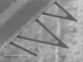
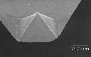
82 Si 3 N 4 Si 3 N 4 Atomic force microscopy Probes: cantilever and tip Si Si 82

83 Atomic force microscopy Contact mode (repulsive mode) F = nn-µn Topography F = k. z - Constant height - Constant load 83
84 Atomic force microscopy Force spectroscopy Repulsive Pull-out force Adhesive 84
85 Atomic force microscopy Tapping mode f ~ f R A = nm 85
")
86 Atomic force microscopy TEM Examples Cork cell walls (contact) A B 86


87 Atomic force microscopy Examples PVD TiN coatings on stainless steel (tapping) 87

 Tip")


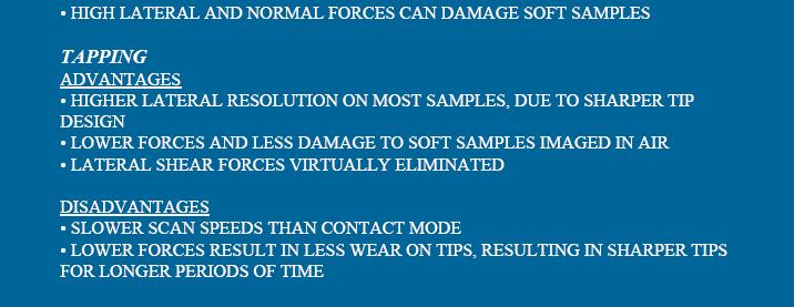
88 Atomic force microscopy Contact vs tapping Hard samples (contact/taping) Soft samples(tapping) Tip damage (tapping) Adsorption layers e.g. water (contact) High scanning speed (contact slow feedback in dynamic mode) 88

89 89 Atomic force microscopy
90 Atomic force microscopy Lateral Force Microscopy (LFM) Cantilever torsion is proportional to height and to friction 90


91 Atomic force microscopy Magnetic/ Electric Force Microscopy (MFM and EFM) Step 1 In a first scan topography is measured under tapping mode Step 2 In a second scan phase, amplitude or frequency changes of the cantilever caused by magnetic or electric interactions are measured. V + - MFM EFM 91


92 Atomic force microscopy MFM example Recording tape CrO 2 Topographic Image Magnetic Force Image 92
93 Atomic force microscopy EFM example - two-component LB-film (NT-MDT) Topography Electric field distribution 93

94 94 Atomic force microscopy
 http://micro.magnet.fsu.")
95 95 Near-Field Scanning Optical Microscopy (NSOM or SNOM)

")


96 Near-Field Scanning Optical Microscopy (NSOM or SNOM) Shear Force Microscopy DNA Scan size: 1.25 µm x1.25 µm 96
 http://www.ntmdt.")
97 Near-Field Scanning Optical Microscopy (NSOM or SNOM) Transmission mode 97
 http://www.ntmdt.")
98 Near-Field Scanning Optical Microscopy (NSOM or SNOM) Reflection mode 98
 http://www.ntmdt.")
99 Near-Field Scanning Optical Microscopy (NSOM or SNOM) Fluorescence mode 99
100 Microscopy techniques for biomaterials Discussion 100 Engenharia Biomédica
SCANNING ELECTRON MICROSCOPY AND X-RAY MICROANALYSIS
 SCANNING ELECTRON MICROSCOPY AND X-RAY MICROANALYSIS Robert Edward Lee Electron Microscopy Center Department of Anatomy and Neurobiology Colorado State University P T R Prentice Hall, Englewood Cliffs,
NanoSpective, Inc Progress Drive Suite 137 Orlando, Florida
 TEM Techniques Summary The TEM is an analytical instrument in which a thin membrane (typically < 100nm) is placed in the path of an energetic and highly coherent beam of electrons. Typical operating voltages
ELECTRON MICROSCOPY. 13:10 16:00, Oct. 6, 2008 Institute of Physics, Academia Sinica. Tung Hsu
 ELECTRON MICROSCOPY 13:10 16:00, Oct. 6, 2008 Institute of Physics, Academia Sinica Tung Hsu Department of Materials Science and Engineering National Tsing Hua University Hsinchu 300, TAIWAN Tel. 03-5742564
Introduction to Transmission Electron Microscopy (Physical Sciences)
") Introduction to Transmission Electron Microscopy (Physical Sciences) Centre for Advanced Microscopy Program 9:30 10:45 Lecture 1 Basics of TEM 10:45 11:00 Morning tea 11:00 12:15 Lecture 2 Diffraction
Introduction to Transmission Electron Microscopy (Physical Sciences) Centre for Advanced Microscopy Program 9:30 10:45 Lecture 1 Basics of TEM 10:45 11:00 Morning tea 11:00 12:15 Lecture 2 Diffraction
NANO 703-Notes. Chapter 9-The Instrument
 1 Chapter 9-The Instrument Illumination (condenser) system Before (above) the sample, the purpose of electron lenses is to form the beam/probe that will illuminate the sample. Our electron source is macroscopic
S200 Course LECTURE 1 TEM
 S200 Course LECTURE 1 TEM Development of Electron Microscopy 1897 Discovery of the electron (J.J. Thompson) 1924 Particle and wave theory (L. de Broglie) 1926 Electromagnetic Lens (H. Busch) 1932 Construction
Chapter 2 Instrumentation for Analytical Electron Microscopy Lecture 7. Chapter 2 CHEM Fall L. Ma
 Chapter 2 Instrumentation for Analytical Electron Microscopy Lecture 7 Outline Electron Sources (Electron Guns) Thermionic: LaB 6 or W Field emission gun: cold or Schottky Lenses Focusing Aberration Probe
Chapter 4 Imaging Lecture 17
 Chapter 4 Imaging Lecture 17 d (110) Imaging Imaging in the TEM Diffraction Contrast in TEM Image HRTEM (High Resolution Transmission Electron Microscopy) Imaging STEM imaging Imaging in the TEM What is
--> Buy True-PDF --> Auto-delivered in 0~10 minutes. JY/T
 Translated English of Chinese Standard: JY/T011-1996 www.chinesestandard.net Sales@ChineseStandard.net INDUSTRY STANDARD OF THE JY PEOPLE S REPUBLIC OF CHINA General rules for transmission electron microscopy
MODULE I SCANNING ELECTRON MICROSCOPE (SEM)
") MODULE I SCANNING ELECTRON MICROSCOPE (SEM) Scanning Electron Microscope (SEM) Initially, the plan of SEM was offered by H. Stintzing in 1927 (a German patent application). His suggested procedure was
MODULE I SCANNING ELECTRON MICROSCOPE (SEM) Scanning Electron Microscope (SEM) Initially, the plan of SEM was offered by H. Stintzing in 1927 (a German patent application). His suggested procedure was
Transmission Electron Microscopy 9. The Instrument. Outline
 Transmission Electron Microscopy 9. The Instrument EMA 6518 Spring 2009 02/25/09 Outline The Illumination System The Objective Lens and Stage Forming Diffraction Patterns and Images Alignment and Stigmation
Transmissions Electron Microscopy (TEM)
") Transmissions Electron Microscopy (TEM) Basic principles Diffraction Imaging Specimen preparation A.E. Gunnæs MENA3100 V17 TEM is based on three possible set of techniqes Diffraction From regions down
Transmissions Electron Microscopy (TEM) Basic principles Diffraction Imaging Specimen preparation A.E. Gunnæs MENA3100 V17 TEM is based on three possible set of techniqes Diffraction From regions down
Transmission electron Microscopy
 Transmission electron Microscopy Image formation of a concave lens in geometrical optics Some basic features of the transmission electron microscope (TEM) can be understood from by analogy with the operation
Observing Microorganisms through a Microscope LIGHT MICROSCOPY: This type of microscope uses visible light to observe specimens. Compound Light Micros
 PHARMACEUTICAL MICROBIOLOGY JIGAR SHAH INSTITUTE OF PHARMACY NIRMA UNIVERSITY Observing Microorganisms through a Microscope LIGHT MICROSCOPY: This type of microscope uses visible light to observe specimens.
VISUAL PHYSICS ONLINE DEPTH STUDY: ELECTRON MICROSCOPES
 VISUAL PHYSICS ONLINE DEPTH STUDY: ELECTRON MICROSCOPES Shortly after the experimental confirmation of the wave properties of the electron, it was suggested that the electron could be used to examine objects
Introduction of New Products
 Field Emission Electron Microscope JEM-3100F For evaluation of materials in the fields of nanoscience and nanomaterials science, TEM is required to provide resolution and analytical capabilities that can
ELECTRON MICROSCOPY AN OVERVIEW
 ELECTRON MICROSCOPY AN OVERVIEW Anjali Priya 1, Abhishek Singh 2, Nikhil Anand Srivastava 3 1,2,3 Department of Electrical & Instrumentation, Sant Longowal Institute of Engg. & Technology, Sangrur, India.
Scanning electron microscope
 Scanning electron microscope 6 th CEMM workshop Maja Koblar, Sc. Eng. Physics Outline The basic principle? What is an electron? Parts of the SEM Electron gun Electromagnetic lenses Apertures Chamber and
Scanning electron microscope
 Scanning electron microscope 5 th CEMM workshop Maja Koblar, Sc. Eng. Physics Outline The basic principle? What is an electron? Parts of the SEM Electron gun Electromagnetic lenses Apertures Detectors
2.Components of an electron microscope. a) vacuum systems, b) electron guns, c) electron optics, d) detectors. Marco Cantoni 021/
 vacuum systems, b) electron guns, c) electron optics, d) detectors. Marco Cantoni 021/") 2.Components of an electron microscope a) vacuum systems, b) electron guns, c) electron optics, d) detectors, 021/693.48.16 Centre Interdisciplinaire de Microscopie Electronique CIME Summary Electron propagation
2.Components of an electron microscope a) vacuum systems, b) electron guns, c) electron optics, d) detectors, 021/693.48.16 Centre Interdisciplinaire de Microscopie Electronique CIME Summary Electron propagation
Introduction to Scanning Electron Microscopy
 Introduction to Scanning Electron Microscopy By: Brandon Cheney Ant s Leg Integrated Circuit Nano-composite This document was created as part of a Senior Project in the Materials Engineering Department
ELECTRON MICROSCOPY. 14:10 17:00, Apr. 3, 2007 Department of Physics, National Taiwan University. Tung Hsu
 ELECTRON MICROSCOPY 14:10 17:00, Apr. 3, 2007 Department of Physics, National Taiwan University Tung Hsu Department of Materials Science and Engineering National Tsinghua University Hsinchu 300, TAIWAN
CHAPTER TWO METALLOGRAPHY & MICROSCOPY
 CHAPTER TWO METALLOGRAPHY & MICROSCOPY 1. INTRODUCTION: Materials characterisation has two main aspects: Accurately measuring the physical, mechanical and chemical properties of materials Accurately measuring
Topics 3b,c Electron Microscopy
 Topics 3b,c Electron Microscopy 1.0 Introduction and History 1.1 Characteristic Information 2.0 Basic Principles 2.1 Electron-Solid Interactions 2.2 Electromagnetic Lenses 2.3 Breakdown of an Electron
2.Components of an electron microscope. a) vacuum systems, b) electron guns, c) electron optics, d) detectors. Marco Cantoni, 021/
 vacuum systems, b) electron guns, c) electron optics, d) detectors. Marco Cantoni, 021/") 2.Components of an electron microscope a) vacuum systems, b) electron guns, c) electron optics, d) detectors Marco Cantoni, 021/693.48.16 Centre Interdisciplinaire de Microscopie Electronique CIME MSE-603
2.Components of an electron microscope a) vacuum systems, b) electron guns, c) electron optics, d) detectors Marco Cantoni, 021/693.48.16 Centre Interdisciplinaire de Microscopie Electronique CIME MSE-603
Scanning Electron Microscopy Basics and Applications
 Scanning Electron Microscopy Basics and Applications Dr. Julia Deuschle Stuttgart Center for Electron Microscopy MPI for Solid State Research Room: 1E15, phone: 0711/ 689-1193 email: j.deuschle@fkf.mpg.de
Chapter 1. Basic Electron Optics (Lecture 2)
") Chapter 1. Basic Electron Optics (Lecture 2) Basic concepts of microscope (Cont ) Fundamental properties of electrons Electron Scattering Instrumentation Basic conceptions of microscope (Cont ) Ray diagram
Chapter 1. Basic Electron Optics (Lecture 2) Basic concepts of microscope (Cont ) Fundamental properties of electrons Electron Scattering Instrumentation Basic conceptions of microscope (Cont ) Ray diagram
Introduction to Electron Microscopy
 Introduction to Electron Microscopy Prof. David Muller, dm24@cornell.edu Rm 274 Clark Hall, 255-4065 Ernst Ruska and Max Knoll built the first electron microscope in 1931 (Nobel Prize to Ruska in 1986)
Microscopy Techniques that make it easy to see things this small.
 Microscopy Techniques that make it easy to see things this small. What is a Microscope? An instrument for viewing objects that are too small to be seen easily by the naked eye. Dutch spectacle-makers Hans
Functions of the SEM subsystems
 Functions of the SEM subsystems Electronic column It consists of an electron gun and two or more electron lenses, which influence the path of electrons traveling down an evacuated tube. The base of the
Fabrication of Probes for High Resolution Optical Microscopy
 Fabrication of Probes for High Resolution Optical Microscopy Physics 564 Applied Optics Professor Andrès La Rosa David Logan May 27, 2010 Abstract Near Field Scanning Optical Microscopy (NSOM) is a technique
Scanning Electron Microscopy. EMSE-515 F. Ernst
 Scanning Electron Microscopy EMSE-515 F. Ernst 1 2 Scanning Electron Microscopy Max Knoll Manfred von Ardenne Manfred von Ardenne Principle of Scanning Electron Microscopy 3 Principle of Scanning Electron
Introduction: Why electrons?
 Introduction: Why electrons? 1 Radiations Visible light X-rays Electrons Neutrons Advantages Not very damaging Easily focused Eye wonderful detector Small wavelength (Angstroms) Good penetration Small
Microscopic Structures
 Microscopic Structures Image Analysis Metal, 3D Image (Red-Green) The microscopic methods range from dark field / bright field microscopy through polarisation- and inverse microscopy to techniques like
Electron
 Electron 1897: Sir Joseph John Thomson (1856-1940) discovered corpuscles small particles with a charge-to-mass ratio over 1000 times greater than that of protons. Plum pudding model : electrons in a sea
Low Voltage Electron Microscope
 LVEM5 Low Voltage Electron Microscope Nanoscale from your benchtop LVEM5 Delong America DELONG INSTRUMENTS COMPACT BUT POWERFUL The LVEM5 is designed to excel across a broad range of applications in material
Microscope anatomy, image formation and resolution
 Microscope anatomy, image formation and resolution Ian Dobbie Buy this book for your lab: D.B. Murphy, "Fundamentals of light microscopy and electronic imaging", ISBN 0-471-25391-X Visit these websites:
Lecture 20: Optical Tools for MEMS Imaging
 MECH 466 Microelectromechanical Systems University of Victoria Dept. of Mechanical Engineering Lecture 20: Optical Tools for MEMS Imaging 1 Overview Optical Microscopes Video Microscopes Scanning Electron
(Refer Slide Time: 00:10)
") Fundamentals of optical and scanning electron microscopy Dr. S. Sankaran Department of Metallurgical and Materials Engineering Indian Institute of Technology, Madras Module 03 Unit-6 Instrumental details
Fundamentals of optical and scanning electron microscopy Dr. S. Sankaran Department of Metallurgical and Materials Engineering Indian Institute of Technology, Madras Module 03 Unit-6 Instrumental details
Chapter Ray and Wave Optics
 109 Chapter Ray and Wave Optics 1. An astronomical telescope has a large aperture to [2002] reduce spherical aberration have high resolution increase span of observation have low dispersion. 2. If two
ELECTRON MICROSCOPY. 09:10 12:00, Oct. 27, 2006 Institute of Physics, Academia Sinica. Tung Hsu
 ELECTRON MICROSCOPY 09:10 12:00, Oct. 27, 2006 Institute of Physics, Academia Sinica Tung Hsu Department of Materials Science and Engineering National Tsinghua University Hsinchu 300, TAIWAN Tel. 03-5742564
Basics of Light Microscopy and Metallography
 ENGR45: Introduction to Materials Spring 2012 Laboratory 8 Basics of Light Microscopy and Metallography In this exercise you will: gain familiarity with the proper use of a research-grade light microscope
Electron Sources, Optics and Detectors
 Thomas LaGrange, Ph.D. Faculty Lecturer and Senior Staff Scientist Electron Sources, Optics and Detectors TEM Doctoral Course MS-637 April 16 th -18 th, 2018 Summary Electron propagation is only possible
The Wave Nature of Light
 The Wave Nature of Light Physics 102 Lecture 7 4 April 2002 Pick up Grating & Foil & Pin 4 Apr 2002 Physics 102 Lecture 7 1 Light acts like a wave! Last week we saw that light travels from place to place
TEM theory Basic optics, image formation and key elements
 Workshop series of Chinese 3DEM community Get acquainted with Cryo-Electron Microscopy: First Chinese Workshop for Structural Biologists TEM theory Basic optics, image formation and key elements Jianlin
SCIENTIFIC INSTRUMENT NEWS. Introduction. Design of the FlexSEM 1000
 SCIENTIFIC INSTRUMENT NEWS 2017 Vol. 9 SEPTEMBER Technical magazine of Electron Microscope and Analytical Instruments. Technical Explanation The FlexSEM 1000: A Scanning Electron Microscope Specializing
OPTICAL SYSTEMS OBJECTIVES
 101 L7 OPTICAL SYSTEMS OBJECTIVES Aims Your aim here should be to acquire a working knowledge of the basic components of optical systems and understand their purpose, function and limitations in terms
Resolution. Diffraction from apertures limits resolution. Rayleigh criterion θ Rayleigh = 1.22 λ/d 1 peak at 2 nd minimum. θ f D
 Microscopy Outline 1. Resolution and Simple Optical Microscope 2. Contrast enhancement: Dark field, Fluorescence (Chelsea & Peter), Phase Contrast, DIC 3. Newer Methods: Scanning Tunneling microscopy (STM),
5. The Scanning Electron Microscope
 Physical Principles of Electron Microscopy 5. The Scanning Electron Microscope Ray Egerton University of Alberta and National Institute of Nanotechnology Edmonton, Canada www.tem-eels.ca regerton@ualberta.ca
Chapter 25. Optical Instruments
 Chapter 25 Optical Instruments Optical Instruments Analysis generally involves the laws of reflection and refraction Analysis uses the procedures of geometric optics To explain certain phenomena, the wave
attosnom I: Topography and Force Images NANOSCOPY APPLICATION NOTE M06 RELATED PRODUCTS G
 APPLICATION NOTE M06 attosnom I: Topography and Force Images Scanning near-field optical microscopy is the outstanding technique to simultaneously measure the topography and the optical contrast of a sample.
Observing Microorganisms through a Microscope
 2016/2/19 PowerPoint Lecture Presentations prepared by Bradley W. Christian, McLennan Community College CHAPTER 3 Observing Microorganisms through a Microscope 1 Figure 3.2 Microscopes and Magnification.
Light Microscopy. Upon completion of this lecture, the student should be able to:
 Light Light microscopy is based on the interaction of light and tissue components and can be used to study tissue features. Upon completion of this lecture, the student should be able to: 1- Explain the
Oct. 30th- Nov. 1st, 2017
 Thomas LaGrange, Ph.D. Faculty Lecturer and Senior Staff Scientist Electron Sources, Optics and Detectors SEM Doctoral Course MS-636 Oct. 30th- Nov. 1st, 2017 Summary Electron propagation is only possible
microscopy A great online resource Molecular Expressions, a Microscope Primer Partha Roy
 Fundamentals of optical microscopy A great online resource Molecular Expressions, a Microscope Primer http://micro.magnet.fsu.edu/primer/index.html Partha Roy 1 Why microscopy Topics Functions of a microscope
Introduction to Light Microscopy. (Image: T. Wittman, Scripps)
") Introduction to Light Microscopy (Image: T. Wittman, Scripps) The Light Microscope Four centuries of history Vibrant current development One of the most widely used research tools A. Khodjakov et al. Major
Introduction to Light Microscopy (Image: T. Wittman, Scripps) The Light Microscope Four centuries of history Vibrant current development One of the most widely used research tools A. Khodjakov et al. Major
Reflection! Reflection and Virtual Image!
 1/30/14 Reflection - wave hits non-absorptive surface surface of a smooth water pool - incident vs. reflected wave law of reflection - concept for all electromagnetic waves - wave theory: reflected back
SECONDARY ELECTRON DETECTION
 SECONDARY ELECTRON DETECTION CAMTEC Workshop Presentation Haitian Xu June 14 th 2010 Introduction SEM Raster scan specimen surface with focused high energy e- beam Signal produced by beam interaction with
OPERATION OF THE HITACHI S-450 SCANNING ELECTRON MICROSCOPE. by Doug Bray Department of Biological Sciences University of Lethbridge
 OPERATION OF THE HITACHI S-450 SCANNING ELECTRON MICROSCOPE by Doug Bray Department of Biological Sciences University of Lethbridge Revised September, 2000 Note: The terms in bold in this document represent
The Nature of Light. Light and Energy
 The Nature of Light Light and Energy - dependent on energy from the sun, directly and indirectly - solar energy intimately associated with existence of life -light absorption: dissipate as heat emitted
Point Spread Function. Confocal Laser Scanning Microscopy. Confocal Aperture. Optical aberrations. Alternative Scanning Microscopy
 Bi177 Lecture 5 Adding the Third Dimension Wide-field Imaging Point Spread Function Deconvolution Confocal Laser Scanning Microscopy Confocal Aperture Optical aberrations Alternative Scanning Microscopy
MSE 460 TEM Lab 2: Basic Alignment and Operation of Microscope
 MSE 460 TEM Lab 2: Basic Alignment and Operation of Microscope Last updated on 1/8/2018 Jinsong Wu, jinsong-wu@northwestern.edu Aims: The aim of this lab is to familiarize you with basic TEM alignment
Chapter 2 The Study of Microbial Structure: Microscopy and Specimen Preparation
 Chapter 2 The Study of Microbial Structure: Microscopy and Specimen Preparation 1 Lenses and the Bending of Light light is refracted (bent) when passing from one medium to another refractive index a measure
Applications of Optics
 Nicholas J. Giordano www.cengage.com/physics/giordano Chapter 26 Applications of Optics Marilyn Akins, PhD Broome Community College Applications of Optics Many devices are based on the principles of optics
Low Voltage Electron Microscope. Nanoscale from your benchtop LVEM5. Delong America
 LVEM5 Low Voltage Electron Microscope Nanoscale from your benchtop LVEM5 Delong America DELONG INSTRUMENTS COMPACT BUT POWERFUL The LVEM5 is designed to excel across a broad range of applications in material
Secondary Electron Detector
 Secondary Electron Detector Fig. 17 Everhart-Thornley Detector (Fig. 7-9, p. 215, Bozzola and Russell) Secondary electrons (SE) are attracted to Faraday cage because of its positive charge. Detector surface
Measurement of Microscopic Three-dimensional Profiles with High Accuracy and Simple Operation
 238 Hitachi Review Vol. 65 (2016), No. 7 Featured Articles Measurement of Microscopic Three-dimensional Profiles with High Accuracy and Simple Operation AFM5500M Scanning Probe Microscope Satoshi Hasumura
Low Voltage Electron Microscope
 LVEM 25 Low Voltage Electron Microscope fast compact powerful Delong America FAST, COMPACT AND POWERFUL The LVEM 25 offers a high-contrast, high-throughput, and compact solution with nanometer resolutions.
Katarina Logg, Kristofer Bodvard, Mikael Käll. Dept. of Applied Physics. 12 September Optical Microscopy. Supervisor s signature:...
 Katarina Logg, Kristofer Bodvard, Mikael Käll Dept. of Applied Physics 12 September 2007 O1 Optical Microscopy Name:.. Date:... Supervisor s signature:... Introduction Over the past decades, the number
Scanning Electron Microscopy
 Scanning Electron Microscopy For the semiconductor industry A tutorial Titel Vorname Nachname Titel Jobtitle, Bereich/Abteilung Overview Scanning Electron microscopy Scanning Electron Microscopy (SEM)
LVEM 25. Low Voltage Electron Mictoscope. fast compact powerful
 LVEM 25 Low Voltage Electron Mictoscope fast compact powerful FAST, COMPACT AND POWERFUL The LVEM 25 offers a high-contrast, high-throughput, and compact solution with nanometer resolutions. All the benefits
Image Formation. Light from distant things. Geometrical optics. Pinhole camera. Chapter 36
 Light from distant things Chapter 36 We learn about a distant thing from the light it generates or redirects. The lenses in our eyes create images of objects our brains can process. This chapter concerns
2014 HTD-E with options
 with options The HT7700 : a user-friendly, ergonomic digital TEM with options User-Friendly r end Design Ambient light operation. Multiple automated functions for alignment, focus and stigmation as standard
FYS 4340/FYS Diffraction Methods & Electron Microscopy. Lecture 9. Imaging Part I. Sandeep Gorantla. FYS 4340/9340 course Autumn
 FYS 4340/FYS 9340 Diffraction Methods & Electron Microscopy Lecture 9 Imaging Part I Sandeep Gorantla FYS 4340/9340 course Autumn 2016 1 Imaging 2 Abbe s principle of imaging Unlike with visible light,
Oct. 30th- Nov. 1st, 2017
 Thomas LaGrange, Ph.D. Faculty Lecturer and Senior Staff Scientist Electron Sources, Optics and Detectors SEM Doctoral Course MS-636 Oct. 30th- Nov. 1st, 2017 Summary Electron propagation is only possible
Scanning Electron Microscopy SEM. Warren Straszheim, PhD MARL, 23 Town Engineering
 Scanning Electron Microscopy SEM Warren Straszheim, PhD MARL, 23 Town Engineering wesaia@iastate.edu 515-294-8187 How it works Create a focused electron beam Accelerate it Scan it across the sample Map
; A=4π(2m) 1/2 /h. exp (Fowler Nordheim Eq.) 2 const
 1/2 /h. exp (Fowler Nordheim Eq.) 2 const") Scanning Tunneling Microscopy (STM) Brief background: In 1981, G. Binnig, H. Rohrer, Ch. Gerber and J. Weibel observed vacuum tunneling of electrons between a sharp tip and a platinum surface. The tunnel
Scanning Tunneling Microscopy (STM) Brief background: In 1981, G. Binnig, H. Rohrer, Ch. Gerber and J. Weibel observed vacuum tunneling of electrons between a sharp tip and a platinum surface. The tunnel
INTRODUCTION THIN LENSES. Introduction. given by the paraxial refraction equation derived last lecture: Thin lenses (19.1) = 1. Double-lens systems
 = 1. Double-lens systems") Chapter 9 OPTICAL INSTRUMENTS Introduction Thin lenses Double-lens systems Aberrations Camera Human eye Compound microscope Summary INTRODUCTION Knowledge of geometrical optics, diffraction and interference,
Chapter 9 OPTICAL INSTRUMENTS Introduction Thin lenses Double-lens systems Aberrations Camera Human eye Compound microscope Summary INTRODUCTION Knowledge of geometrical optics, diffraction and interference,
Tissue Preparation ORGANISM IMAGE TISSUE PREPARATION. 1) Fixation: halts cell metabolism, preserves cell/tissue structure
 Fixation: halts cell metabolism, preserves cell/tissue structure") Lab starts this week! ANNOUNCEMENTS - Tuesday or Wednesday 1:25 ISB 264 - Read Lab 1: Microscopy and Imaging (see Web Page) - Getting started on Lab Group project - Organ for investigation - Lab project
Lab starts this week! ANNOUNCEMENTS - Tuesday or Wednesday 1:25 ISB 264 - Read Lab 1: Microscopy and Imaging (see Web Page) - Getting started on Lab Group project - Organ for investigation - Lab project
Spectroscopy in the UV and Visible: Instrumentation. Spectroscopy in the UV and Visible: Instrumentation
 Spectroscopy in the UV and Visible: Instrumentation Typical UV-VIS instrument 1 Source - Disperser Sample (Blank) Detector Readout Monitor the relative response of the sample signal to the blank Transmittance
Full-screen mode Popup controls. Overview of the microscope user interface, TEM User Interface and TIA on the left and EDS on the right
 Quick Guide to Operating FEI Titan Themis G2 200 (S)TEM: TEM mode Susheng Tan Nanoscale Fabrication and Characterization Facility, University of Pittsburgh Office: M104/B01 Benedum Hall, 412-383-5978,
attocfm I for Surface Quality Inspection NANOSCOPY APPLICATION NOTE M01 RELATED PRODUCTS G
 APPLICATION NOTE M01 attocfm I for Surface Quality Inspection Confocal microscopes work by scanning a tiny light spot on a sample and by measuring the scattered light in the illuminated volume. First,
ECEN 4606, UNDERGRADUATE OPTICS LAB
 ECEN 4606, UNDERGRADUATE OPTICS LAB Lab 2: Imaging 1 the Telescope Original Version: Prof. McLeod SUMMARY: In this lab you will become familiar with the use of one or more lenses to create images of distant
Test Review # 8. Physics R: Form TR8.17A. Primary colors of light
 Physics R: Form TR8.17A TEST 8 REVIEW Name Date Period Test Review # 8 Light and Color. Color comes from light, an electromagnetic wave that travels in straight lines in all directions from a light source
Confocal Imaging Through Scattering Media with a Volume Holographic Filter
 Confocal Imaging Through Scattering Media with a Volume Holographic Filter Michal Balberg +, George Barbastathis*, Sergio Fantini % and David J. Brady University of Illinois at Urbana-Champaign, Urbana,
Recent results from the JEOL JEM-3000F FEGTEM in Oxford
 Recent results from the JEOL JEM-3000F FEGTEM in Oxford R.E. Dunin-Borkowski a, J. Sloan b, R.R. Meyer c, A.I. Kirkland c,d and J. L. Hutchison a a b c d Department of Materials, Parks Road, Oxford OX1
Applied Optics. , Physics Department (Room #36-401) , ,
 , ,") Applied Optics Professor, Physics Department (Room #36-401) 2290-0923, 019-539-0923, shsong@hanyang.ac.kr Office Hours Mondays 15:00-16:30, Wednesdays 15:00-16:30 TA (Ph.D. student, Room #36-415) 2290-0921,
Applied Optics Professor, Physics Department (Room #36-401) 2290-0923, 019-539-0923, shsong@hanyang.ac.kr Office Hours Mondays 15:00-16:30, Wednesdays 15:00-16:30 TA (Ph.D. student, Room #36-415) 2290-0921,
GIST OF THE UNIT BASED ON DIFFERENT CONCEPTS IN THE UNIT (BRIEFLY AS POINT WISE). RAY OPTICS
. RAY OPTICS") 209 GIST OF THE UNIT BASED ON DIFFERENT CONCEPTS IN THE UNIT (BRIEFLY AS POINT WISE). RAY OPTICS Reflection of light: - The bouncing of light back into the same medium from a surface is called reflection
209 GIST OF THE UNIT BASED ON DIFFERENT CONCEPTS IN THE UNIT (BRIEFLY AS POINT WISE). RAY OPTICS Reflection of light: - The bouncing of light back into the same medium from a surface is called reflection
Outline: Introduction: What is SPM, history STM AFM Image treatment Advanced SPM techniques Applications in semiconductor research and industry
 1 Outline: Introduction: What is SPM, history STM AFM Image treatment Advanced SPM techniques Applications in semiconductor research and industry 2 Back to our solutions: The main problem: How to get nm
Manufacturing Metrology Team
 The Team has a range of state-of-the-art equipment for the measurement of surface texture and form. We are happy to discuss potential measurement issues and collaborative research Manufacturing Metrology
Lateral Force: F L = k L * x
 Scanning Force Microscopy (SFM): Conventional SFM Application: Topography measurements Force: F N = k N * k N Ppring constant: Spring deflection: Pieo Scanner Interaction or force dampening field Contact
Heisenberg) relation applied to space and transverse wavevector
 relation applied to space and transverse wavevector") 2. Optical Microscopy 2.1 Principles A microscope is in principle nothing else than a simple lens system for magnifying small objects. The first lens, called the objective, has a short focal length (a
2. Optical Microscopy 2.1 Principles A microscope is in principle nothing else than a simple lens system for magnifying small objects. The first lens, called the objective, has a short focal length (a
Microscopy. Matti Hotokka Department of Physical Chemistry Åbo Akademi University
 Microscopy Matti Hotokka Department of Physical Chemistry Åbo Akademi University What s coming Anatomy of a microscope Modes of illumination Practicalities Special applications Basic microscope Ocular
Very short introduction to light microscopy and digital imaging
 Very short introduction to light microscopy and digital imaging Hernan G. Garcia August 1, 2005 1 Light Microscopy Basics In this section we will briefly describe the basic principles of operation and
PHY 431 Homework Set #5 Due Nov. 20 at the start of class
 PHY 431 Homework Set #5 Due Nov. 0 at the start of class 1) Newton s rings (10%) The radius of curvature of the convex surface of a plano-convex lens is 30 cm. The lens is placed with its convex side down
ABC Math Student Copy. N. May ABC Math Student Copy. Physics Week 13(Sem. 2) Name. Light Chapter Summary Cont d 2
 Name. Light Chapter Summary Cont d 2") Page 1 of 12 Physics Week 13(Sem. 2) Name Light Chapter Summary Cont d 2 Lens Abberation Lenses can have two types of abberation, spherical and chromic. Abberation occurs when the rays forming an image
Page 1 of 12 Physics Week 13(Sem. 2) Name Light Chapter Summary Cont d 2 Lens Abberation Lenses can have two types of abberation, spherical and chromic. Abberation occurs when the rays forming an image
OPTICAL PRINCIPLES OF MICROSCOPY. Interuniversity Course 28 December 2003 Aryeh M. Weiss Bar Ilan University
 OPTICAL PRINCIPLES OF MICROSCOPY Interuniversity Course 28 December 2003 Aryeh M. Weiss Bar Ilan University FOREWORD This slide set was originally presented at the ISM Workshop on Theoretical and Experimental
Lecture 2: Geometrical Optics. Geometrical Approximation. Lenses. Mirrors. Optical Systems. Images and Pupils. Aberrations.
 Lecture 2: Geometrical Optics Outline 1 Geometrical Approximation 2 Lenses 3 Mirrors 4 Optical Systems 5 Images and Pupils 6 Aberrations Christoph U. Keller, Leiden Observatory, keller@strw.leidenuniv.nl
A few concepts in TEM and STEM explained
 A few concepts in TEM and STEM explained Martin Ek November 23, 2011 1 Introduction This is a collection of short, qualitative explanations of key concepts in TEM and STEM. Most of them are beyond what
:... resolution is about 1.4 μm, assumed an excitation wavelength of 633 nm and a numerical aperture of 0.65 at 633 nm.
 PAGE 30 & 2008 2007 PRODUCT CATALOG Confocal Microscopy - CFM fundamentals :... Over the years, confocal microscopy has become the method of choice for obtaining clear, three-dimensional optical images