2.Components of an electron microscope. a) vacuum systems, b) electron guns, c) electron optics, d) detectors. Marco Cantoni 021/
|
|
|
- Ariel Henry
- 5 years ago
- Views:
Transcription
1 2.Components of an electron microscope a) vacuum systems, b) electron guns, c) electron optics, d) detectors, 021/ Centre Interdisciplinaire de Microscopie Electronique CIME Summary Electron propagation is only possible through vacuum. The vacuum level varies in the different areas of an electron microscope. The highest vacuum level (<10-7 Pa or 10-9 mbar) is required in the gun where electrons are emitted through field emission. Also the specimen area requires a high vacuum level especially for chemical analysis when the electron beam is resting for a longer time in the same area. Hydrocarbon build up (contamination) on the observed area is often the result of a low system vacuum level. Turbomolecular and oil-diffusion pumps for high vaccum cannot work against atmospheric pressure and need a mechanical prevaccum pump in order to function. Electron beams can either be generated by thermal emission (thermionic sources, cheap) or field emission. Only field emission sources can provide the necessary low energy spread and coherence for modern high resolution electron microscopy and electron spectroscopy. Electrons are focused by simple round magnetic lenses which properties resemble the optical properties of a wine glass. Unlike in light optics the wavelength (2pm for 300kV) is not the resolution limiting factor. However lens aberrations and instabilities of the electronics (lens currents etc.) limit the resolution of even the best and most expensive transmission electron microscopes to about 50pm. Recording an image means detecting electrons. Depending on their energy electrons can be detected by different detectors. A high detector efficiency and a high signal to noise ratio allows faster recording and reduces the exposure (beam damage) of the sample to the electron beam. A high linearity and high dynamic range permits to quantify images and to record high and low intensities in one image (important for diffraction experiments).
 Detector(s) common SEM and TEM Specific for")
 Mechanical pump Secondary vacuum (<10-4 Pa) Oil diffusion pump Turbomolecular pump High and ultra-high")
2 Components of an electron microscope Vacuum system! Source: electron gun Lenses and apertures Sample holder (stage) Detector(s) common SEM and TEM Specific for each technique Pumping system Primary vacuum (>0.1 Pa) Mechanical pump Secondary vacuum (<10-4 Pa) Oil diffusion pump Turbomolecular pump High and ultra-high vacuum Gun & specimen area (<10-6 Pa) Ion getter pump Cold trap Vaccum level in space: 1 Pa at 100km above earth surface


")
3 Primary vacuum Rotary vane pump Uses oil noisy Secondary vacuum Oil diffusion pump Vibration free Contamination possible oil vapor High pumping capacity (>500 l/s) Best with cold trap


4 Secondary vacuum Turbomolecular pump Rotation speed rpm Magnetic bearings Pumping volumes l/s High / Ultra-high vacuum Ion getter pump no vibrations No exit: improves vacuum!
 Electric field")

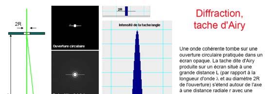
5 SOURCES (gun) LaB 6 Cathode Emission of electrons metal vacuum (with electrical field) Electric field Thermionic emission Shottky emission field-enhanced thermionic emission (10 8 V/m) Extended Shottky emission thermally assisted field emission Cold field emission tunnel effect (quantum tunnelling) temperature
 temperature Electron gun Important parameters Emitted current, energy Energy dispersion Brightness current per surface")
6 Emission of electrons metal vacuum (with electrical field) Electric field Thermionic emission Shottky emission field-enhanced thermionic emission (10 8 V/m) Extended Shottky emission thermally assisted field emission Cold field emission tunnel effect (quantum tunnelling) temperature Electron gun Important parameters Emitted current, energy Energy dispersion Brightness current per surface unit and solid angle Coupling to the column the gun incorporates often a first lens (Wehnelt, gun lens)


7 Thermionic gun Tungsten wire heated up to 2800K LaB 6 crystal heated to 1900K Advantage simple, cheap no high vacuum required maintenance friendly Disadvantages low brightness high energy dispersion large source size (30um)

 after 8 hrs Field emission guns First anode (extractor) Some kv 5.")
8 Field emission guns Cathods Cold field emission (E 10 9 V/m) W monocristal with sharp tip tip radius ~100nm Thermally assisted emission: Shottky effect W/Zr tip at K Advantages Small energy dispersion (<0.4eV) high coherence, high brightness -> higher resolution at lower energies Disadvantages expensive high vacuum necessary cold emission needs flushing (cleaning) after 8 hrs Field emission guns First anode (extractor) Some kv V/m Second anode Final acceleration Grounded Characteristics Tip and anodes form an electrostatic condensor Cross-over (source) is virtual Ø~5nm


9 Ion gun (FIB) Most common: LIMS Liquid Metal Ion Source W tip Liquid metal wets the tip through surface tension and electrostatic force Ionization and emission by field effect (~10 10 V/m) High brightness Small emitting surface (Taylor cone) Small Ion probes (~5nm) possible: FIB Focused Ion Beam LMIS Source: FEI Beam Technology Division


10 Optics, basics tiré de Carter/Williams Optics, basics Object plane Focal plane Image plane Carter/Williams
 mode DIFFRACTION mode")
11 Optics, basics tiré de Carter/Williams TEM: transmitted beam, diffracted beams Projector lens system, TEM TEM: Intermediate and projector lenses Projection of the back focal plane to the screen diffraction mode Projection of the image plane to the screen image mode (haute resolution) mode DIFFRACTION mode IMAGE
 mode DIFFRACTION mode")

12 Projector lens system, TEM TEM: Intermediate and projector lenses Projection of the back focal plane to the screen diffraction mode Projection of the image plane to the screen image mode (haute resolution) mode DIFFRACTION mode IMAGE Lenses for electrons Light: glass lenses deflection of light through changing refraction index Charged particles Lorentz Force! Electrostatic lenses Magnetic lenses Particularity: Variable focus Tunable correctors (astigmatisme)

13 Electrons in a magnetic field Optical axis Homogeneus field, small Component of v // B almost unchanged Component of v B: v r << v Spiral with radius r = m vr/eb All electrons crossing the axis in one point are focused into the same point, v r Focal length depends on B increasing B lowers f Magnetic lens Field with rotational symmetry Lorenz Force : F = -e v ^ B e on optical axis: F = 0 e not on optical axis : deviated optical axis: symmetry axis Scherzer 1936: Magnetic lens with rotational symmetry: Aberration coefficients: C s : spherical C c : chromatical Always positive!! Resolution limit: D res 3/ 4 1/ Cs Example: = nm, C s = 1 mm D res = = 1.8Å


14 Magnetic lens iron e-beam Electron optics: no sharp interface at lens «surface» No divergent lens! Electron beam diverges by itself Electrostatic repulsion Pole piece coil multi-poles lenses Correction of aberrations Pole piece metal cone that confines the magnetic field Image rotation! Aberrations: Lens aberrations sperical and chromatical aberrations Astigmatism Can be corrected or minimised Physical limits Diffraction effect Clichés: P.-A. Buffat

 Spherical aberration")


15 chromatical aberration Focal length varies with energy critical for non-monochromatic beams (advantage for FE guns) Spherical aberration Focal length depends on the distance from optical axis Image of the object is dispersed along the optical axis Circle of least confusion d s = ½ C s 3


16 Aberrations: astigmatism Astigmatism: focal length varies in different planes. correctors Astigmatism: Light optics: correction with cylindrical lenses Electron optics: Correction with quadrupole lenses: 2 quadrupole lenses under 45 degree allow to control strenght and direction of correction Spherical Aberration: Light optics: correction with combination of convergent and divergent lenses Electron optics: Correction with hexapole or quadrupole and octopole lenses Cs-corrector
17 Aberrations: diffraction Résolution SEM Limite SEM modèrne
18 Resolution: SEM Résolution (nm) Low voltage, high resolution Basse tension/haute résolution: - Observation observation of de the la surface real surface réelle - Uncoated échantillons samples non-métallisés - faible endommagement dû au Very faisceau little beam damage FE 1985 LaB 6 W Haute High voltage, tension/haute high resolution résolution: - effets de bord Edge effects, fine details not - resolved détails fins non-résolus - fort endommagement dû au Beam faisceau damage Tension d'accélération (kv)
2.Components of an electron microscope. a) vacuum systems, b) electron guns, c) electron optics, d) detectors. Marco Cantoni, 021/
 vacuum systems, b) electron guns, c) electron optics, d) detectors. Marco Cantoni, 021/") 2.Components of an electron microscope a) vacuum systems, b) electron guns, c) electron optics, d) detectors Marco Cantoni, 021/693.48.16 Centre Interdisciplinaire de Microscopie Electronique CIME MSE-603
2.Components of an electron microscope a) vacuum systems, b) electron guns, c) electron optics, d) detectors Marco Cantoni, 021/693.48.16 Centre Interdisciplinaire de Microscopie Electronique CIME MSE-603
Oct. 30th- Nov. 1st, 2017
 Thomas LaGrange, Ph.D. Faculty Lecturer and Senior Staff Scientist Electron Sources, Optics and Detectors SEM Doctoral Course MS-636 Oct. 30th- Nov. 1st, 2017 Summary Electron propagation is only possible
Oct. 30th- Nov. 1st, 2017
 Thomas LaGrange, Ph.D. Faculty Lecturer and Senior Staff Scientist Electron Sources, Optics and Detectors SEM Doctoral Course MS-636 Oct. 30th- Nov. 1st, 2017 Summary Electron propagation is only possible
Electron Sources, Optics and Detectors
 Thomas LaGrange, Ph.D. Faculty Lecturer and Senior Staff Scientist Electron Sources, Optics and Detectors TEM Doctoral Course MS-637 April 16 th -18 th, 2018 Summary Electron propagation is only possible
Scanning electron microscope
 Scanning electron microscope 6 th CEMM workshop Maja Koblar, Sc. Eng. Physics Outline The basic principle? What is an electron? Parts of the SEM Electron gun Electromagnetic lenses Apertures Chamber and
Scanning electron microscope
 Scanning electron microscope 5 th CEMM workshop Maja Koblar, Sc. Eng. Physics Outline The basic principle? What is an electron? Parts of the SEM Electron gun Electromagnetic lenses Apertures Detectors
SCANNING ELECTRON MICROSCOPY AND X-RAY MICROANALYSIS
 SCANNING ELECTRON MICROSCOPY AND X-RAY MICROANALYSIS Robert Edward Lee Electron Microscopy Center Department of Anatomy and Neurobiology Colorado State University P T R Prentice Hall, Englewood Cliffs,
Scanning Electron Microscopy. EMSE-515 F. Ernst
 Scanning Electron Microscopy EMSE-515 F. Ernst 1 2 Scanning Electron Microscopy Max Knoll Manfred von Ardenne Manfred von Ardenne Principle of Scanning Electron Microscopy 3 Principle of Scanning Electron
S200 Course LECTURE 1 TEM
 S200 Course LECTURE 1 TEM Development of Electron Microscopy 1897 Discovery of the electron (J.J. Thompson) 1924 Particle and wave theory (L. de Broglie) 1926 Electromagnetic Lens (H. Busch) 1932 Construction
Cs-corrector. Felix de Haas
 Cs-corrector. Felix de Haas Content Non corrector systems Lens aberrations and how to minimize? Corrector systems How is it done? Lens aberrations Spherical aberration Astigmatism Coma Chromatic Quality
Introduction: Why electrons?
 Introduction: Why electrons? 1 Radiations Visible light X-rays Electrons Neutrons Advantages Not very damaging Easily focused Eye wonderful detector Small wavelength (Angstroms) Good penetration Small
p q p f f f q f p q f NANO 703-Notes Chapter 5-Magnification and Electron Sources
 Chapter 5-agnification and Electron Sources Lens equation Let s first consider the properties of an ideal lens. We want rays diverging from a point on an object in front of the lens to converge to a corresponding
Transmissions Electron Microscopy (TEM)
") Transmissions Electron Microscopy (TEM) Basic principles Diffraction Imaging Specimen preparation A.E. Gunnæs MENA3100 V17 TEM is based on three possible set of techniqes Diffraction From regions down
Transmissions Electron Microscopy (TEM) Basic principles Diffraction Imaging Specimen preparation A.E. Gunnæs MENA3100 V17 TEM is based on three possible set of techniqes Diffraction From regions down
Chapter Ray and Wave Optics
 109 Chapter Ray and Wave Optics 1. An astronomical telescope has a large aperture to [2002] reduce spherical aberration have high resolution increase span of observation have low dispersion. 2. If two
Scanning Electron Microscopy Basics and Applications
 Scanning Electron Microscopy Basics and Applications Dr. Julia Deuschle Stuttgart Center for Electron Microscopy MPI for Solid State Research Room: 1E15, phone: 0711/ 689-1193 email: j.deuschle@fkf.mpg.de
Tecnai on-line help manual --
 Tecnai on-line help Alignments 1 Tecnai on-line help manual -- Alignments Table of Contents 1 Alignments in the Tecnai microscope...5 2 Alignment procedures...6 3 Introduction to electron optics...11 3.1
Transmission Electron Microscopy 9. The Instrument. Outline
 Transmission Electron Microscopy 9. The Instrument EMA 6518 Spring 2009 02/25/09 Outline The Illumination System The Objective Lens and Stage Forming Diffraction Patterns and Images Alignment and Stigmation
Low Voltage Electron Microscope
 LVEM5 Low Voltage Electron Microscope Nanoscale from your benchtop LVEM5 Delong America DELONG INSTRUMENTS COMPACT BUT POWERFUL The LVEM5 is designed to excel across a broad range of applications in material
Introduction to Scanning Electron Microscopy
 Introduction to Scanning Electron Microscopy By: Brandon Cheney Ant s Leg Integrated Circuit Nano-composite This document was created as part of a Senior Project in the Materials Engineering Department
MODULE I SCANNING ELECTRON MICROSCOPE (SEM)
") MODULE I SCANNING ELECTRON MICROSCOPE (SEM) Scanning Electron Microscope (SEM) Initially, the plan of SEM was offered by H. Stintzing in 1927 (a German patent application). His suggested procedure was
MODULE I SCANNING ELECTRON MICROSCOPE (SEM) Scanning Electron Microscope (SEM) Initially, the plan of SEM was offered by H. Stintzing in 1927 (a German patent application). His suggested procedure was
Nanotechnology and material science Lecture V
 Most widely used nanoscale microscopy. Based on possibility to create bright electron beam with sub-nm spot size. History: Ernst Ruska (1931), Nobel Prize (1986) For visible light λ=400-700nm, for electrons
Introduction of New Products
 Field Emission Electron Microscope JEM-3100F For evaluation of materials in the fields of nanoscience and nanomaterials science, TEM is required to provide resolution and analytical capabilities that can
Low Voltage Electron Microscope
 LVEM 25 Low Voltage Electron Microscope fast compact powerful Delong America FAST, COMPACT AND POWERFUL The LVEM 25 offers a high-contrast, high-throughput, and compact solution with nanometer resolutions.
Fabrication of Probes for High Resolution Optical Microscopy
 Fabrication of Probes for High Resolution Optical Microscopy Physics 564 Applied Optics Professor Andrès La Rosa David Logan May 27, 2010 Abstract Near Field Scanning Optical Microscopy (NSOM) is a technique
LVEM 25. Low Voltage Electron Mictoscope. fast compact powerful
 LVEM 25 Low Voltage Electron Mictoscope fast compact powerful FAST, COMPACT AND POWERFUL The LVEM 25 offers a high-contrast, high-throughput, and compact solution with nanometer resolutions. All the benefits
Chapter 1. Basic Electron Optics (Lecture 2)
") Chapter 1. Basic Electron Optics (Lecture 2) Basic concepts of microscope (Cont ) Fundamental properties of electrons Electron Scattering Instrumentation Basic conceptions of microscope (Cont ) Ray diagram
Chapter 1. Basic Electron Optics (Lecture 2) Basic concepts of microscope (Cont ) Fundamental properties of electrons Electron Scattering Instrumentation Basic conceptions of microscope (Cont ) Ray diagram
Low Voltage Electron Microscope. Nanoscale from your benchtop LVEM5. Delong America
 LVEM5 Low Voltage Electron Microscope Nanoscale from your benchtop LVEM5 Delong America DELONG INSTRUMENTS COMPACT BUT POWERFUL The LVEM5 is designed to excel across a broad range of applications in material
ELECTRON MICROSCOPY. 13:10 16:00, Oct. 6, 2008 Institute of Physics, Academia Sinica. Tung Hsu
 ELECTRON MICROSCOPY 13:10 16:00, Oct. 6, 2008 Institute of Physics, Academia Sinica Tung Hsu Department of Materials Science and Engineering National Tsing Hua University Hsinchu 300, TAIWAN Tel. 03-5742564
WIEN Software for Design of Columns Containing Wien Filters and Multipole Lenses
 WIEN Software for Design of Columns Containing Wien Filters and Multipole Lenses An integrated workplace for analysing and optimising the column optics Base Package (WIEN) Handles round lenses, quadrupoles,
ELECTRON MICROSCOPY AN OVERVIEW
 ELECTRON MICROSCOPY AN OVERVIEW Anjali Priya 1, Abhishek Singh 2, Nikhil Anand Srivastava 3 1,2,3 Department of Electrical & Instrumentation, Sant Longowal Institute of Engg. & Technology, Sangrur, India.
25 cm. 60 cm. 50 cm. 40 cm.
 Geometrical Optics 7. The image formed by a plane mirror is: (a) Real. (b) Virtual. (c) Erect and of equal size. (d) Laterally inverted. (e) B, c, and d. (f) A, b and c. 8. A real image is that: (a) Which
ELECTRON MICROSCOPY. 14:10 17:00, Apr. 3, 2007 Department of Physics, National Taiwan University. Tung Hsu
 ELECTRON MICROSCOPY 14:10 17:00, Apr. 3, 2007 Department of Physics, National Taiwan University Tung Hsu Department of Materials Science and Engineering National Tsinghua University Hsinchu 300, TAIWAN
Design and Application of a Quadrupole Detector for Low-Voltage Scanning Electron Mcroscopy
 SCANNING Vol. 8, 294-299 (1986) 0 FACM. Inc. Received: August 29, 1986 Original Paper Design and Application of a Quadrupole Detector for Low-Voltage Scanning Electron Mcroscopy R. Schmid and M. Brunner"
Design and fabrication of a scanning electron microscope using a finite element analysis for electron optical system
 Journal of Mechanical Science and Technology 22 (2008) 1734~1746 Journal of Mechanical Science and Technology www.springerlink.com/content/1738-494x DOI 10.1007/s12206-008-0317-9 Design and fabrication
Functions of the SEM subsystems
 Functions of the SEM subsystems Electronic column It consists of an electron gun and two or more electron lenses, which influence the path of electrons traveling down an evacuated tube. The base of the
Big League Cryogenics and Vacuum The LHC at CERN
 Big League Cryogenics and Vacuum The LHC at CERN A typical astronomical instrument must maintain about one cubic meter at a pressure of
High Resolution Transmission Electron Microscopy (HRTEM) Summary 4/11/2018. Thomas LaGrange Faculty Lecturer and Senior Staff Scientist
 Summary 4/11/2018. Thomas LaGrange Faculty Lecturer and Senior Staff Scientist") Thomas LaGrange Faculty Lecturer and Senior Staff Scientist High Resolution Transmission Electron Microscopy (HRTEM) Doctoral Course MS-637 April 16-18th, 2018 Summary Contrast in TEM images results from
Thomas LaGrange Faculty Lecturer and Senior Staff Scientist High Resolution Transmission Electron Microscopy (HRTEM) Doctoral Course MS-637 April 16-18th, 2018 Summary Contrast in TEM images results from
Reflection! Reflection and Virtual Image!
 1/30/14 Reflection - wave hits non-absorptive surface surface of a smooth water pool - incident vs. reflected wave law of reflection - concept for all electromagnetic waves - wave theory: reflected back
Introduction to Electron Microscopy
 Introduction to Electron Microscopy Prof. David Muller, dm24@cornell.edu Rm 274 Clark Hall, 255-4065 Ernst Ruska and Max Knoll built the first electron microscope in 1931 (Nobel Prize to Ruska in 1986)
A Tutorial on Electron Microscopy
 A Tutorial on Electron Microscopy Jian-Min (Jim) Zuo Mat. Sci. Eng. and Seitz-Materials Research Lab., UIUC Outline of This Tutorial I. Science and opportunities of electron microscopy II. The basic TEM,
CHAPTER TWO METALLOGRAPHY & MICROSCOPY
 CHAPTER TWO METALLOGRAPHY & MICROSCOPY 1. INTRODUCTION: Materials characterisation has two main aspects: Accurately measuring the physical, mechanical and chemical properties of materials Accurately measuring
MSE 460 TEM Lab 2: Basic Alignment and Operation of Microscope
 MSE 460 TEM Lab 2: Basic Alignment and Operation of Microscope Last updated on 1/8/2018 Jinsong Wu, jinsong-wu@northwestern.edu Aims: The aim of this lab is to familiarize you with basic TEM alignment
VISUAL PHYSICS ONLINE DEPTH STUDY: ELECTRON MICROSCOPES
 VISUAL PHYSICS ONLINE DEPTH STUDY: ELECTRON MICROSCOPES Shortly after the experimental confirmation of the wave properties of the electron, it was suggested that the electron could be used to examine objects
Chapter 2 Instrumentation for Analytical Electron Microscopy Lecture 7. Chapter 2 CHEM Fall L. Ma
 Chapter 2 Instrumentation for Analytical Electron Microscopy Lecture 7 Outline Electron Sources (Electron Guns) Thermionic: LaB 6 or W Field emission gun: cold or Schottky Lenses Focusing Aberration Probe
Introduction to Transmission Electron Microscopy (Physical Sciences)
") Introduction to Transmission Electron Microscopy (Physical Sciences) Centre for Advanced Microscopy Program 9:30 10:45 Lecture 1 Basics of TEM 10:45 11:00 Morning tea 11:00 12:15 Lecture 2 Diffraction
Introduction to Transmission Electron Microscopy (Physical Sciences) Centre for Advanced Microscopy Program 9:30 10:45 Lecture 1 Basics of TEM 10:45 11:00 Morning tea 11:00 12:15 Lecture 2 Diffraction
ELECTRON MICROSCOPY. 09:10 12:00, Oct. 27, 2006 Institute of Physics, Academia Sinica. Tung Hsu
 ELECTRON MICROSCOPY 09:10 12:00, Oct. 27, 2006 Institute of Physics, Academia Sinica Tung Hsu Department of Materials Science and Engineering National Tsinghua University Hsinchu 300, TAIWAN Tel. 03-5742564
Electron
 Electron 1897: Sir Joseph John Thomson (1856-1940) discovered corpuscles small particles with a charge-to-mass ratio over 1000 times greater than that of protons. Plum pudding model : electrons in a sea
TEM theory Basic optics, image formation and key elements
 Workshop series of Chinese 3DEM community Get acquainted with Cryo-Electron Microscopy: First Chinese Workshop for Structural Biologists TEM theory Basic optics, image formation and key elements Jianlin
The Nature of Light. Light and Energy
 The Nature of Light Light and Energy - dependent on energy from the sun, directly and indirectly - solar energy intimately associated with existence of life -light absorption: dissipate as heat emitted
Applied Optics. , Physics Department (Room #36-401) , ,
 , ,") Applied Optics Professor, Physics Department (Room #36-401) 2290-0923, 019-539-0923, shsong@hanyang.ac.kr Office Hours Mondays 15:00-16:30, Wednesdays 15:00-16:30 TA (Ph.D. student, Room #36-415) 2290-0921,
Applied Optics Professor, Physics Department (Room #36-401) 2290-0923, 019-539-0923, shsong@hanyang.ac.kr Office Hours Mondays 15:00-16:30, Wednesdays 15:00-16:30 TA (Ph.D. student, Room #36-415) 2290-0921,
Introduction to Electron Microscopy-II
 Introduction to Electron Microscopy-II Prof. David Muller, dm24@cornell.edu Rm 274 Clark Hall, 255-4065 Ernst Ruska and Max Knoll built the first electron microscope in 1931 (Nobel Prize to Ruska in 1986)
Topics 3b,c Electron Microscopy
 Topics 3b,c Electron Microscopy 1.0 Introduction and History 1.1 Characteristic Information 2.0 Basic Principles 2.1 Electron-Solid Interactions 2.2 Electromagnetic Lenses 2.3 Breakdown of an Electron
Recent results from the JEOL JEM-3000F FEGTEM in Oxford
 Recent results from the JEOL JEM-3000F FEGTEM in Oxford R.E. Dunin-Borkowski a, J. Sloan b, R.R. Meyer c, A.I. Kirkland c,d and J. L. Hutchison a a b c d Department of Materials, Parks Road, Oxford OX1
EE119 Introduction to Optical Engineering Fall 2009 Final Exam. Name:
 EE119 Introduction to Optical Engineering Fall 2009 Final Exam Name: SID: CLOSED BOOK. THREE 8 1/2 X 11 SHEETS OF NOTES, AND SCIENTIFIC POCKET CALCULATOR PERMITTED. TIME ALLOTTED: 180 MINUTES Fundamental
Filter & Spectrometer Electron Optics
 Filter & Spectrometer Electron Optics Parameters Affecting Practical Performance Daniel Moonen & Harold A. Brink Did Something Go Wrong? 30 20 10 0 500 600 700 800 900 1000 1100 ev 1 Content The Prism
Lenses. A transparent object used to change the path of light Examples: Human eye Eye glasses Camera Microscope Telescope
 SNC2D Lenses A transparent object used to change the path of light Examples: Human eye Eye glasses Camera Microscope Telescope Reading stones used by monks, nuns, and scholars ~1000 C.E. Lenses THERE ARE
CS-TEM vs CS-STEM. FEI Titan CIME EPFL. Duncan Alexander EPFL-CIME
 CS-TEM vs CS-STEM Duncan Alexander EPFL-CIME 1 FEI Titan Themis @ CIME EPFL 60 300 kv Monochromator High brightness X-FEG Probe Cs-corrected: 0.7 Å @ 300 kv Image Cs-corrected: 0.7 Å @ 300 kv Super-X EDX
NANO 703-Notes. Chapter 9-The Instrument
 1 Chapter 9-The Instrument Illumination (condenser) system Before (above) the sample, the purpose of electron lenses is to form the beam/probe that will illuminate the sample. Our electron source is macroscopic
Transmission electron Microscopy
 Transmission electron Microscopy Image formation of a concave lens in geometrical optics Some basic features of the transmission electron microscope (TEM) can be understood from by analogy with the operation
SUBJECT: PHYSICS. Use and Succeed.
 SUBJECT: PHYSICS I hope this collection of questions will help to test your preparation level and useful to recall the concepts in different areas of all the chapters. Use and Succeed. Navaneethakrishnan.V
Mohammed A. Hussein *
 International Journal of Physics, 216, Vol. 4, No. 5, 13-134 Available online at http://pubs.sciepub.com/ijp/4/5/3 Science and Education Publishing DOI:1.12691/ijp-4-5-3 Effect of the Geometrical Shape
Microscope. Dr. Leena Barhate Department of Microbiology M.J.College, Jalgaon
 Microscope Dr. Leena Barhate Department of Microbiology M.J.College, Jalgaon Acknowledgement http://www.cerebromente.org.br/n17/histor y/neurons1_i.htm Google Images http://science.howstuffworks.com/lightmicroscope1.htm
Name. Light Chapter Summary Cont d. Refraction
 Page 1 of 17 Physics Week 12(Sem. 2) Name Light Chapter Summary Cont d with a smaller index of refraction to a material with a larger index of refraction, the light refracts towards the normal line. Also,
CS-TEM vs CS-STEM. FEI Titan CIME EPFL. Duncan Alexander EPFL-CIME
 CS-TEM vs CS-STEM Duncan Alexander EPFL-CIME 1 FEI Titan Themis @ CIME EPFL 60 300 kv Monochromator High brightness X-FEG Probe Cs-corrected: 0.7 Å @ 300 kv Image Cs-corrected: 0.7 Å @ 300 kv Super-X EDX
Study on Imaging Quality of Water Ball Lens
 2017 2nd International Conference on Mechatronics and Information Technology (ICMIT 2017) Study on Imaging Quality of Water Ball Lens Haiyan Yang1,a,*, Xiaopan Li 1,b, 1,c Hao Kong, 1,d Guangyang Xu and1,eyan
ELECTRON OPTICS. Prof. John G. King Dr. John W. Coleman Dr. Edward H. Jacobsen. Graduate Students. Steven R. Jost Norman D. Punsky
 II. ELECTRON OPTICS Academic and Research Staff Prof. John G. King Dr. John W. Coleman Dr. Edward H. Jacobsen Graduate Students Steven R. Jost Norman D. Punsky A. HIGH-RESOLUTION HIGH-CONTRAST ELECTRON
Section A Conceptual and application type questions. 1 Which is more observable diffraction of light or sound? Justify. (1)
") INDIAN SCHOOL MUSCAT Department of Physics Class : XII Physics Worksheet - 6 (2017-2018) Chapter 9 and 10 : Ray Optics and wave Optics Section A Conceptual and application type questions 1 Which is more
INDIAN SCHOOL MUSCAT Department of Physics Class : XII Physics Worksheet - 6 (2017-2018) Chapter 9 and 10 : Ray Optics and wave Optics Section A Conceptual and application type questions 1 Which is more
Observing Microorganisms through a Microscope LIGHT MICROSCOPY: This type of microscope uses visible light to observe specimens. Compound Light Micros
 PHARMACEUTICAL MICROBIOLOGY JIGAR SHAH INSTITUTE OF PHARMACY NIRMA UNIVERSITY Observing Microorganisms through a Microscope LIGHT MICROSCOPY: This type of microscope uses visible light to observe specimens.
A Portable Scanning Electron Microscope Column Design Based on the Use of Permanent Magnets
 SCANNING VOL. 20, 87 91 (1998) Received October 8, 1997 FAMS, Inc. Accepted with revision November 9, 1997 A Portable Scanning Electron Microscope Column Design Based on the Use of Permanent Magnets A.
NanoSpective, Inc Progress Drive Suite 137 Orlando, Florida
 TEM Techniques Summary The TEM is an analytical instrument in which a thin membrane (typically < 100nm) is placed in the path of an energetic and highly coherent beam of electrons. Typical operating voltages
ECEN 4606, UNDERGRADUATE OPTICS LAB
 ECEN 4606, UNDERGRADUATE OPTICS LAB Lab 2: Imaging 1 the Telescope Original Version: Prof. McLeod SUMMARY: In this lab you will become familiar with the use of one or more lenses to create images of distant
PHYS 160 Astronomy. When analyzing light s behavior in a mirror or lens, it is helpful to use a technique called ray tracing.
 Optics Introduction In this lab, we will be exploring several properties of light including diffraction, reflection, geometric optics, and interference. There are two sections to this lab and they may
How to choose a Scanning Electron Microscope (SEM)
") www.lambdaphoto.co.uk E-guide How to choose a Scanning Electron Microscope (SEM) Providing guidance in the selection of the right microscope for your research Distribution in the UK & Ireland Table of
www.lambdaphoto.co.uk E-guide How to choose a Scanning Electron Microscope (SEM) Providing guidance in the selection of the right microscope for your research Distribution in the UK & Ireland Table of
Lecture 4: Geometrical Optics 2. Optical Systems. Images and Pupils. Rays. Wavefronts. Aberrations. Outline
 Lecture 4: Geometrical Optics 2 Outline 1 Optical Systems 2 Images and Pupils 3 Rays 4 Wavefronts 5 Aberrations Christoph U. Keller, Leiden University, keller@strw.leidenuniv.nl Lecture 4: Geometrical
MSE 595T Transmission Electron Microscopy. Laboratory III TEM Imaging - I
 MSE 595T Basic Transmission Electron Microscopy TEM Imaging - I Purpose The purpose of this lab is to: 1. Make fine adjustments to the microscope alignment 2. Obtain a diffraction pattern 3. Obtain an
TSBB09 Image Sensors 2018-HT2. Image Formation Part 1
 TSBB09 Image Sensors 2018-HT2 Image Formation Part 1 Basic physics Electromagnetic radiation consists of electromagnetic waves With energy That propagate through space The waves consist of transversal
--> Buy True-PDF --> Auto-delivered in 0~10 minutes. JY/T
 Translated English of Chinese Standard: JY/T011-1996 www.chinesestandard.net Sales@ChineseStandard.net INDUSTRY STANDARD OF THE JY PEOPLE S REPUBLIC OF CHINA General rules for transmission electron microscopy
NANO MODIFICATION OF THE W(100)/ZrO ELECTRON EMITTER TIP USING REACTIVE ION ETCHING
/ZrO ELECTRON EMITTER TIP USING REACTIVE ION ETCHING") NANO MODIFICATION OF THE W(100)/ZrO ELECTRON EMITTER TIP USING REACTIVE ION ETCHING Miroslav HORÁČEK, František MATĚJKA, Vladimír KOLAŘÍK, Milan MATĚJKA, Michal URBÁNEK Ústav přístrojové techniky AV ČR,
NANO MODIFICATION OF THE W(100)/ZrO ELECTRON EMITTER TIP USING REACTIVE ION ETCHING Miroslav HORÁČEK, František MATĚJKA, Vladimír KOLAŘÍK, Milan MATĚJKA, Michal URBÁNEK Ústav přístrojové techniky AV ČR,
Nanotechnology in Consumer Products
 Nanotechnology in Consumer Products Advances in Transmission Electron Microscopy Friday, April 21, 2017 October 31, 2014 The webinar will begin at 1pm Eastern Time Click here to watch the webinar recording
Indiana University JEM-3200FS
 Indiana University JEM-3200FS Installation Specification Model: JEM 3200FS Serial Number: EM 15000013 Objective Lens Configuration: High Resolution Pole Piece (HRP) JEOL Engineer: Michael P. Van Etten
Scanning Electron Microscopy SEM. Warren Straszheim, PhD MARL, 23 Town Engineering
 Scanning Electron Microscopy SEM Warren Straszheim, PhD MARL, 23 Town Engineering wesaia@iastate.edu 515-294-8187 How it works Create a focused electron beam Accelerate it Scan it across the sample Map
CH. 23 Mirrors and Lenses HW# 6, 7, 9, 11, 13, 21, 25, 31, 33, 35
 CH. 23 Mirrors and Lenses HW# 6, 7, 9, 11, 13, 21, 25, 31, 33, 35 Mirrors Rays of light reflect off of mirrors, and where the reflected rays either intersect or appear to originate from, will be the location
Schottky Emission VP FE-SEM
 Schottky Emission VP FE-SEM Variable Pressure The Scanning Electron Microscope (SEM) has played an important role for many years for research and development of advanced materials in the leading edge of
Lecture 20: Optical Tools for MEMS Imaging
 MECH 466 Microelectromechanical Systems University of Victoria Dept. of Mechanical Engineering Lecture 20: Optical Tools for MEMS Imaging 1 Overview Optical Microscopes Video Microscopes Scanning Electron
Chapter 18 Optical Elements
 Chapter 18 Optical Elements GOALS When you have mastered the content of this chapter, you will be able to achieve the following goals: Definitions Define each of the following terms and use it in an operational
Lab 2 Geometrical Optics
 Lab 2 Geometrical Optics March 22, 202 This material will span much of 2 lab periods. Get through section 5.4 and time permitting, 5.5 in the first lab. Basic Equations Lensmaker s Equation for a thin
LVEM 25. Low Voltage Electron Microscope Fast Compact Powerful.... your way to electron microscopy
 LVEM 25 Low Voltage Electron Microscope Fast Compact Powerful... your way to electron microscopy INTRODUCING THE LVEM 25 High Contrast & High Resolution Unmatched contrast of biologic and light material
1) An electromagnetic wave is a result of electric and magnetic fields acting together. T 1)
 An electromagnetic wave is a result of electric and magnetic fields acting together. T 1)") Exam 3 Review Name TRUE/FALSE. Write 'T' if the statement is true and 'F' if the statement is false. 1) An electromagnetic wave is a result of electric and magnetic fields acting together. T 1) 2) Electromagnetic
Exam 3 Review Name TRUE/FALSE. Write 'T' if the statement is true and 'F' if the statement is false. 1) An electromagnetic wave is a result of electric and magnetic fields acting together. T 1) 2) Electromagnetic
Full-screen mode Popup controls. Overview of the microscope user interface, TEM User Interface and TIA on the left and EDS on the right
 Quick Guide to Operating FEI Titan Themis G2 200 (S)TEM: TEM mode Susheng Tan Nanoscale Fabrication and Characterization Facility, University of Pittsburgh Office: M104/B01 Benedum Hall, 412-383-5978,
INDEX OF REFRACTION index of refraction n = c/v material index of refraction n
 INDEX OF REFRACTION The index of refraction (n) of a material is the ratio of the speed of light in vacuuo (c) to the speed of light in the material (v). n = c/v Indices of refraction for any materials
Titan on-line help manual -- Working with a FEG
 1 manual -- Working with a FEG Table of Contents 1 FEG Safety... 2 1.1 The column valves... 2 2 FEG States... 2 3 Starting the FEG... 4 4 Shutting the FEG down... 6 5 FEG Design... 6 5.1 Electron source...
OPTICAL SYSTEMS OBJECTIVES
 101 L7 OPTICAL SYSTEMS OBJECTIVES Aims Your aim here should be to acquire a working knowledge of the basic components of optical systems and understand their purpose, function and limitations in terms
Test Review # 8. Physics R: Form TR8.17A. Primary colors of light
 Physics R: Form TR8.17A TEST 8 REVIEW Name Date Period Test Review # 8 Light and Color. Color comes from light, an electromagnetic wave that travels in straight lines in all directions from a light source
Introduction to Light Microscopy. (Image: T. Wittman, Scripps)
") Introduction to Light Microscopy (Image: T. Wittman, Scripps) The Light Microscope Four centuries of history Vibrant current development One of the most widely used research tools A. Khodjakov et al. Major
Introduction to Light Microscopy (Image: T. Wittman, Scripps) The Light Microscope Four centuries of history Vibrant current development One of the most widely used research tools A. Khodjakov et al. Major
HOLIDAY HOME WORK PHYSICS CLASS-12B AUTUMN BREAK 2018
 HOLIDAY HOME WK PHYSICS CLASS-12B AUTUMN BREAK 2018 NOTE: 1. THESE QUESTIONS ARE FROM PREVIOUS YEAR BOARD PAPERS FROM 2009-2018 CHAPTERS EMI,AC,OPTICS(BUT TRY TO SOLVE ONLY NON-REPEATED QUESTION) QUESTION
EE119 Introduction to Optical Engineering Spring 2002 Final Exam. Name:
 EE119 Introduction to Optical Engineering Spring 2002 Final Exam Name: SID: CLOSED BOOK. FOUR 8 1/2 X 11 SHEETS OF NOTES, AND SCIENTIFIC POCKET CALCULATOR PERMITTED. TIME ALLOTTED: 180 MINUTES Fundamental
Chapter 25. Optical Instruments
 Chapter 25 Optical Instruments Optical Instruments Analysis generally involves the laws of reflection and refraction Analysis uses the procedures of geometric optics To explain certain phenomena, the wave
Mirrors, Lenses &Imaging Systems
 Mirrors, Lenses &Imaging Systems We describe the path of light as straight-line rays And light rays from a very distant point arrive parallel 145 Phys 24.1 Mirrors Standing away from a plane mirror shows
Lecture PowerPoint. Chapter 25 Physics: Principles with Applications, 6 th edition Giancoli
 Lecture PowerPoint Chapter 25 Physics: Principles with Applications, 6 th edition Giancoli 2005 Pearson Prentice Hall This work is protected by United States copyright laws and is provided solely for the
APPLICATION NOTE
 THE PHYSICS BEHIND TAG OPTICS TECHNOLOGY AND THE MECHANISM OF ACTION OF APPLICATION NOTE 12-001 USING SOUND TO SHAPE LIGHT Page 1 of 6 Tutorial on How the TAG Lens Works This brief tutorial explains the