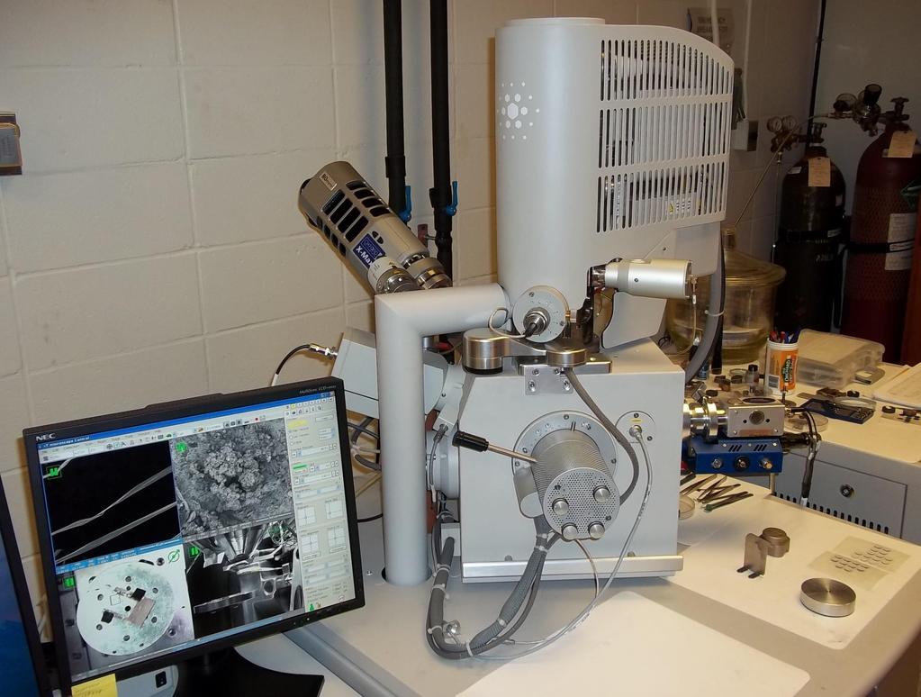
Scanning Electron Microscopy SEM. Warren Straszheim, PhD MARL, 23 Town Engineering
|
|
|
- Jade Leonard
- 5 years ago
- Views:
Transcription
1 Scanning Electron Microscopy SEM Warren Straszheim, PhD MARL, 23 Town Engineering
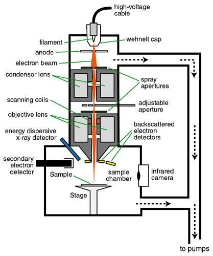
2 How it works Create a focused electron beam Accelerate it Scan it across the sample Map detector output to screen
3
4
5 Create an electron beam Three main types of guns of increasing brightness and coherence Tungsten LaB6 Field Emission
6 Accelerate the beam Requires vacuum to support the voltage to prevent scattering
7 Focus the beam lenses and apertures Wehnelt/Gun Condenser lens Objective lens
8 Benefits of SEM Shorter wavelength higher resolution (0.1 nm electron at 10 kev vs 500 nm for light) Longer working distance greater depth of focus Generally intuitive image interpretation (super magnifying glass) Scanned beam perfect parfocality Wealth of signals: SE BSE, X-ray, voltage Energetic beam - microanalysis
9 Limitations of SEM First surface technique limited penetration (can t see through contamination) Vacuum requirement Conductivity requirement
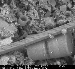
10 Sample preparation Generally minimal Clean and dry Cut sample to fit and show structure of interest Secure sample (tape, glue, clamp) Embed or polish for cross sections Coat with metal or carbon (optional)

11 Auger electrons Secondary electrons Backscattered electrons Characteristic x-rays Continuum x-rays Cathodoluminescence Absorbed current Available signals
 allows more to escape brighter")
12 Contrast mechanism: Topography Secondary electrons have a limited escape depth many are created but few escape A tilted (more vertical surface) allows more to escape brighter signal

13 Extended depth of focus

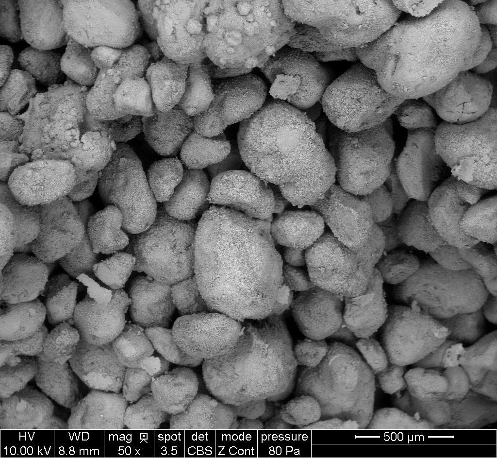
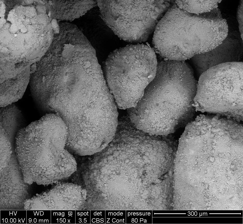
14 Magnification range of less than 50x to 100s of kx
15 Continuous zoom from low magnification to high magnification
16
17
18
19
20
21
, and")
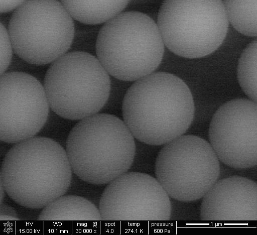
22 By the way, this was a non-conductive sample High-vac, low-vac (variable pressure), and environmental modes
23


24 Image Interpretation Illumination Detection Line of sight
25 Contrast mechanism: Atomic number Higher atomic number/electron density leads to greater secondary electron yield (coat samples with metal) greater backscattering coefficient Atomic number is the only contrast mechanism for polished samples

26 What signal should you use? SE or BSE
27

28 What is the magnification? 240,000x...
29 or 127,000x?

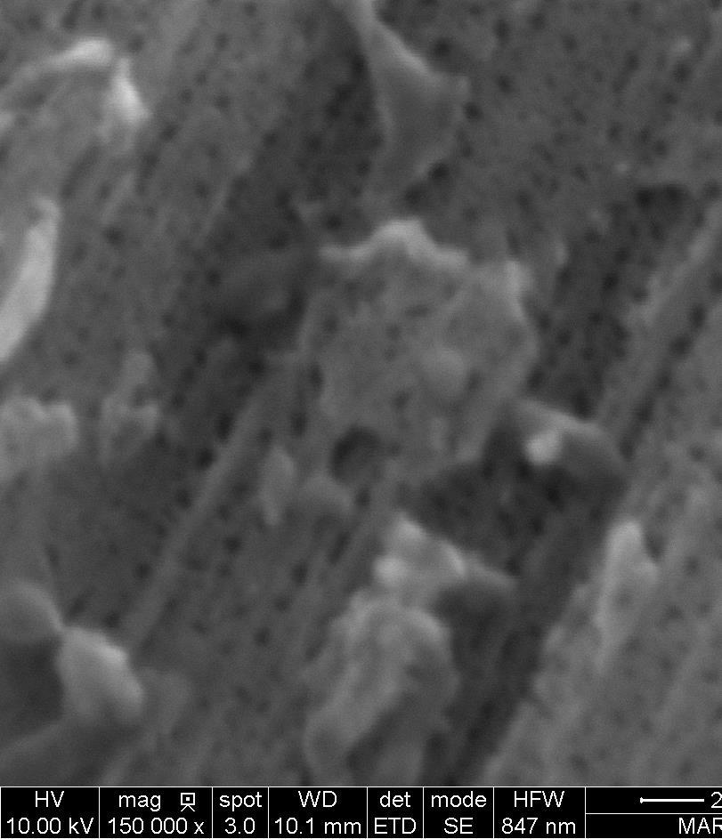
30 Horizontal field width (HFW) = 1000um Magnification = Display width/hfw Mag * HFW = Display width 240,000 x 1000um = 240 mm = 9.5 inches 127,000 x 1000um = 127 mm = 5.0 inches I use a 5-inch Polaroid print as the standard. Other sizes are fake magnification.
31 Resolution/Quality/Speed Pick two Small beam (spot size) leads to better spatial resolution but fewer electrons Bigger beam leads to more signal quality (less noise) but also less resolution Dwell time can be adjusted widely High resolution images are worthless if you can t see the detail through all of the noise
32 Other issues Astigmatism - range of focal lengths Charging - unstable imaging Contamination obscures features of interest Unstable specimens moving targets

33 Charging leading to flattening of SE image

34 BSE image is somewhat more immune to charging

35 Oil leftover from cleaning

36 SEM images the first surface, be that sample, contamination, or surfactant
37 The Importance of Cleanliness Any organic residue left on the sample will build up and obscure the sample with time.

38 BSE imaging may be better at showing the true size

39 Contamination layer builds up and shows in SE

40 Contamination build-up after examination at 150kx

41 Contamination is still visible at 15kx

42 Residue is visible even at 5000x. Longer exposure leads to more build up. Even short exposures lead to contamination.
43 As-received 100kx Cleaned with plasma
44 As-received 150kx Cleaned with plasma

45 Anatomic considerations: bit depth Where can you distinguish gray levels?
46 256 levels, 8-bit
47 128 levels, 7-bit
48 64 levels, 6-bit
49 32 levels, 5 bit
50 16 levels, 4-bit
51 8 levels, 3-bit
52 Anatomic considerations: Pixel density How many pixels are enough? What s the difference between pixels and dots per inch?
53 1024 pixels
54 512 pixels
55 256 pixels
56 128 pixels
57
58 PPI versus DPI (for when editors gets fussy) PPI = pixels per inch, how we describe images DPI = dots per inch, how printers describe files It takes about 8x8 dots to render 1 gray pixel Therefore a 1600 dpi requirement is met by a 1024-pixel image printed no more than 5 inches wide.
59 Environmental Mode Variable pressure mode used for nonconductive or out-gassing samples Environmental mode used to maintain sample at equilibrium (micro-grapes) Various gas choices (water, air, reducing) Heating and cooling options (-25C to 1000C)
60
61
Scanning Electron Microscopy. EMSE-515 F. Ernst
 Scanning Electron Microscopy EMSE-515 F. Ernst 1 2 Scanning Electron Microscopy Max Knoll Manfred von Ardenne Manfred von Ardenne Principle of Scanning Electron Microscopy 3 Principle of Scanning Electron
SCANNING ELECTRON MICROSCOPY AND X-RAY MICROANALYSIS
 SCANNING ELECTRON MICROSCOPY AND X-RAY MICROANALYSIS Robert Edward Lee Electron Microscopy Center Department of Anatomy and Neurobiology Colorado State University P T R Prentice Hall, Englewood Cliffs,
Functions of the SEM subsystems
 Functions of the SEM subsystems Electronic column It consists of an electron gun and two or more electron lenses, which influence the path of electrons traveling down an evacuated tube. The base of the
Secondary Electron Detector
 Secondary Electron Detector Fig. 17 Everhart-Thornley Detector (Fig. 7-9, p. 215, Bozzola and Russell) Secondary electrons (SE) are attracted to Faraday cage because of its positive charge. Detector surface
MODULE I SCANNING ELECTRON MICROSCOPE (SEM)
") MODULE I SCANNING ELECTRON MICROSCOPE (SEM) Scanning Electron Microscope (SEM) Initially, the plan of SEM was offered by H. Stintzing in 1927 (a German patent application). His suggested procedure was
MODULE I SCANNING ELECTRON MICROSCOPE (SEM) Scanning Electron Microscope (SEM) Initially, the plan of SEM was offered by H. Stintzing in 1927 (a German patent application). His suggested procedure was
Scanning electron microscope
 Scanning electron microscope 5 th CEMM workshop Maja Koblar, Sc. Eng. Physics Outline The basic principle? What is an electron? Parts of the SEM Electron gun Electromagnetic lenses Apertures Detectors
Scanning electron microscope
 Scanning electron microscope 6 th CEMM workshop Maja Koblar, Sc. Eng. Physics Outline The basic principle? What is an electron? Parts of the SEM Electron gun Electromagnetic lenses Apertures Chamber and
SECONDARY ELECTRON DETECTION
 SECONDARY ELECTRON DETECTION CAMTEC Workshop Presentation Haitian Xu June 14 th 2010 Introduction SEM Raster scan specimen surface with focused high energy e- beam Signal produced by beam interaction with
Chapter 1. Basic Electron Optics (Lecture 2)
") Chapter 1. Basic Electron Optics (Lecture 2) Basic concepts of microscope (Cont ) Fundamental properties of electrons Electron Scattering Instrumentation Basic conceptions of microscope (Cont ) Ray diagram
Chapter 1. Basic Electron Optics (Lecture 2) Basic concepts of microscope (Cont ) Fundamental properties of electrons Electron Scattering Instrumentation Basic conceptions of microscope (Cont ) Ray diagram
Low Voltage Electron Microscope
 LVEM5 Low Voltage Electron Microscope Nanoscale from your benchtop LVEM5 Delong America DELONG INSTRUMENTS COMPACT BUT POWERFUL The LVEM5 is designed to excel across a broad range of applications in material
Standard Operating Procedure for the Amray 1810 Scanning Electron Microscope Version: 29 NOVEMBER 2014
 Standard Operating Procedure for the Amray 1810 Scanning Electron Microscope Version: 29 NOVEMBER 2014 1. Utility Requirements a. System power is supplied by two 120 VAC/20 A circuits. When doing maintenance
Introduction: Why electrons?
 Introduction: Why electrons? 1 Radiations Visible light X-rays Electrons Neutrons Advantages Not very damaging Easily focused Eye wonderful detector Small wavelength (Angstroms) Good penetration Small
ZEISS EVO SOP. May 2017 ELECTRON OPTICS
 ZEISS EVO SOP May 2017 ELECTRON OPTICS The patented EVO column is the area of the SEM, where electrons are emitted, accelerated, deflected, focused, and scanned. Main characteristics of the EVO optics
ELECTRON MICROSCOPY. 13:10 16:00, Oct. 6, 2008 Institute of Physics, Academia Sinica. Tung Hsu
 ELECTRON MICROSCOPY 13:10 16:00, Oct. 6, 2008 Institute of Physics, Academia Sinica Tung Hsu Department of Materials Science and Engineering National Tsing Hua University Hsinchu 300, TAIWAN Tel. 03-5742564
S200 Course LECTURE 1 TEM
 S200 Course LECTURE 1 TEM Development of Electron Microscopy 1897 Discovery of the electron (J.J. Thompson) 1924 Particle and wave theory (L. de Broglie) 1926 Electromagnetic Lens (H. Busch) 1932 Construction
Low Voltage Electron Microscope. Nanoscale from your benchtop LVEM5. Delong America
 LVEM5 Low Voltage Electron Microscope Nanoscale from your benchtop LVEM5 Delong America DELONG INSTRUMENTS COMPACT BUT POWERFUL The LVEM5 is designed to excel across a broad range of applications in material
Scanning Electron Microscopy
 Scanning Electron Microscopy For the semiconductor industry A tutorial Titel Vorname Nachname Titel Jobtitle, Bereich/Abteilung Overview Scanning Electron microscopy Scanning Electron Microscopy (SEM)
5. The Scanning Electron Microscope
 Physical Principles of Electron Microscopy 5. The Scanning Electron Microscope Ray Egerton University of Alberta and National Institute of Nanotechnology Edmonton, Canada www.tem-eels.ca regerton@ualberta.ca
ELECTRON MICROSCOPY. 14:10 17:00, Apr. 3, 2007 Department of Physics, National Taiwan University. Tung Hsu
 ELECTRON MICROSCOPY 14:10 17:00, Apr. 3, 2007 Department of Physics, National Taiwan University Tung Hsu Department of Materials Science and Engineering National Tsinghua University Hsinchu 300, TAIWAN
Visibility of Detail
 Visibility of Detail Radiographic Quality Quality radiographic images represents the, and information is for diagnosis. The of the anatomic structures and the accuracy of their ( ) determine the overall
OPERATION OF THE HITACHI S-450 SCANNING ELECTRON MICROSCOPE. by Doug Bray Department of Biological Sciences University of Lethbridge
 OPERATION OF THE HITACHI S-450 SCANNING ELECTRON MICROSCOPE by Doug Bray Department of Biological Sciences University of Lethbridge Revised September, 2000 Note: The terms in bold in this document represent
Observing Microorganisms through a Microscope LIGHT MICROSCOPY: This type of microscope uses visible light to observe specimens. Compound Light Micros
 PHARMACEUTICAL MICROBIOLOGY JIGAR SHAH INSTITUTE OF PHARMACY NIRMA UNIVERSITY Observing Microorganisms through a Microscope LIGHT MICROSCOPY: This type of microscope uses visible light to observe specimens.
The light microscope
 What is a microscope? The microscope is an essential tool in modern biology. It allows us to view structural details of organs, tissue, and cells not visible to the naked eye. The microscope should always
Transmission Electron Microscopy 9. The Instrument. Outline
 Transmission Electron Microscopy 9. The Instrument EMA 6518 Spring 2009 02/25/09 Outline The Illumination System The Objective Lens and Stage Forming Diffraction Patterns and Images Alignment and Stigmation
Topics 3b,c Electron Microscopy
 Topics 3b,c Electron Microscopy 1.0 Introduction and History 1.1 Characteristic Information 2.0 Basic Principles 2.1 Electron-Solid Interactions 2.2 Electromagnetic Lenses 2.3 Breakdown of an Electron
Introduction to Scanning Electron Microscopy
 Introduction to Scanning Electron Microscopy By: Brandon Cheney Ant s Leg Integrated Circuit Nano-composite This document was created as part of a Senior Project in the Materials Engineering Department
Unit Two Part II MICROSCOPY
 Unit Two Part II MICROSCOPY AVERETT 1 0 /9/2013 1 MICROSCOPES Microscopes are devices that produce magnified images of structures that are too small to see with the unaided eye Humans cannot see objects
(Refer Slide Time: 00:10)
") Fundamentals of optical and scanning electron microscopy Dr. S. Sankaran Department of Metallurgical and Materials Engineering Indian Institute of Technology, Madras Module 03 Unit-6 Instrumental details
Fundamentals of optical and scanning electron microscopy Dr. S. Sankaran Department of Metallurgical and Materials Engineering Indian Institute of Technology, Madras Module 03 Unit-6 Instrumental details
VISUAL PHYSICS ONLINE DEPTH STUDY: ELECTRON MICROSCOPES
 VISUAL PHYSICS ONLINE DEPTH STUDY: ELECTRON MICROSCOPES Shortly after the experimental confirmation of the wave properties of the electron, it was suggested that the electron could be used to examine objects
Lecture 20: Optical Tools for MEMS Imaging
 MECH 466 Microelectromechanical Systems University of Victoria Dept. of Mechanical Engineering Lecture 20: Optical Tools for MEMS Imaging 1 Overview Optical Microscopes Video Microscopes Scanning Electron
Chapter 2 The Study of Microbial Structure: Microscopy and Specimen Preparation
 Chapter 2 The Study of Microbial Structure: Microscopy and Specimen Preparation 1 Lenses and the Bending of Light light is refracted (bent) when passing from one medium to another refractive index a measure
Figure 3.4 Approximate size of various types of cells. ~10 um. Red Blood Cells = mm 1500 um. Width of penny Pearson Education, Inc.
 Figure 3.4 Approximate size of various types of cells. ~10 um Red Blood Cells 1.5mm 1500 um Width of penny = 1500 Figure 4.3 The limits of resolution (and some representative objects within those ranges)
NANO 703-Notes. Chapter 9-The Instrument
 1 Chapter 9-The Instrument Illumination (condenser) system Before (above) the sample, the purpose of electron lenses is to form the beam/probe that will illuminate the sample. Our electron source is macroscopic
ELECTRON MICROSCOPY AN OVERVIEW
 ELECTRON MICROSCOPY AN OVERVIEW Anjali Priya 1, Abhishek Singh 2, Nikhil Anand Srivastava 3 1,2,3 Department of Electrical & Instrumentation, Sant Longowal Institute of Engg. & Technology, Sangrur, India.
Module 4B7: VLSI Design, Technology, and CAD. Scanning Electron Microscopical Examination of CMOS Integrated Circuit
 Engineering Tripos Part IIB FOURTH YEAR Module 4B7: VLSI Design, Technology, and CAD Laboratory Experiment Dr D Holburn and Mr B Breton Scanning Electron Microscopical Examination of CMOS Integrated Circuit
Low Voltage Electron Microscope
 LVEM 25 Low Voltage Electron Microscope fast compact powerful Delong America FAST, COMPACT AND POWERFUL The LVEM 25 offers a high-contrast, high-throughput, and compact solution with nanometer resolutions.
LVEM 25. Low Voltage Electron Mictoscope. fast compact powerful
 LVEM 25 Low Voltage Electron Mictoscope fast compact powerful FAST, COMPACT AND POWERFUL The LVEM 25 offers a high-contrast, high-throughput, and compact solution with nanometer resolutions. All the benefits
Choosing the Right Accelerating Voltage for SEM (An Introduction for Beginners)
") Microscopy101 Choosing the Right Accelerating Voltage for SEM (An Introduction for Beginners) V.M. Dusevich*, J.H. Purk, and J.D. Eick University of Missouri Kansas City, School of Dentistry, 650 E. 25
Microscopy101 Choosing the Right Accelerating Voltage for SEM (An Introduction for Beginners) V.M. Dusevich*, J.H. Purk, and J.D. Eick University of Missouri Kansas City, School of Dentistry, 650 E. 25
p q p f f f q f p q f NANO 703-Notes Chapter 5-Magnification and Electron Sources
 Chapter 5-agnification and Electron Sources Lens equation Let s first consider the properties of an ideal lens. We want rays diverging from a point on an object in front of the lens to converge to a corresponding
Scanning Electron Microscopy Basics and Applications
 Scanning Electron Microscopy Basics and Applications Dr. Julia Deuschle Stuttgart Center for Electron Microscopy MPI for Solid State Research Room: 1E15, phone: 0711/ 689-1193 email: j.deuschle@fkf.mpg.de
SCIENTIFIC INSTRUMENT NEWS. Introduction. Design of the FlexSEM 1000
 SCIENTIFIC INSTRUMENT NEWS 2017 Vol. 9 SEPTEMBER Technical magazine of Electron Microscope and Analytical Instruments. Technical Explanation The FlexSEM 1000: A Scanning Electron Microscope Specializing
How to choose a Scanning Electron Microscope (SEM)
") www.lambdaphoto.co.uk E-guide How to choose a Scanning Electron Microscope (SEM) Providing guidance in the selection of the right microscope for your research Distribution in the UK & Ireland Table of
www.lambdaphoto.co.uk E-guide How to choose a Scanning Electron Microscope (SEM) Providing guidance in the selection of the right microscope for your research Distribution in the UK & Ireland Table of
Imaging Carbon Nanotubes Magdalena Preciado López, David Zahora, Monica Plisch
 Imaging Carbon Nanotubes Magdalena Preciado López, David Zahora, Monica Plisch I. Introduction In this lab you will image your carbon nanotube sample from last week with an atomic force microscope. You
CHAPTER TWO METALLOGRAPHY & MICROSCOPY
 CHAPTER TWO METALLOGRAPHY & MICROSCOPY 1. INTRODUCTION: Materials characterisation has two main aspects: Accurately measuring the physical, mechanical and chemical properties of materials Accurately measuring
Nanotechnology and material science Lecture V
 Most widely used nanoscale microscopy. Based on possibility to create bright electron beam with sub-nm spot size. History: Ernst Ruska (1931), Nobel Prize (1986) For visible light λ=400-700nm, for electrons
Schottky Emission VP FE-SEM
 Schottky Emission VP FE-SEM Variable Pressure The Scanning Electron Microscope (SEM) has played an important role for many years for research and development of advanced materials in the leading edge of
Variable microinspection system. system125
 Variable microinspection system system125 Variable micro-inspection system Characteristics Large fields, high NA The variable microinspection system mag.x system125 stands out from conventional LD inspection
MICROSCOPE LAB. Resolving Power How well specimen detail is preserved during the magnifying process.
 AP BIOLOGY Cells ACTIVITY #2 MICROSCOPE LAB OBJECTIVES 1. Demonstrate proper care and use of a compound microscope. 2. Identify the parts of the microscope and describe the function of each part. 3. Compare
2.Components of an electron microscope. a) vacuum systems, b) electron guns, c) electron optics, d) detectors. Marco Cantoni, 021/
 vacuum systems, b) electron guns, c) electron optics, d) detectors. Marco Cantoni, 021/") 2.Components of an electron microscope a) vacuum systems, b) electron guns, c) electron optics, d) detectors Marco Cantoni, 021/693.48.16 Centre Interdisciplinaire de Microscopie Electronique CIME MSE-603
2.Components of an electron microscope a) vacuum systems, b) electron guns, c) electron optics, d) detectors Marco Cantoni, 021/693.48.16 Centre Interdisciplinaire de Microscopie Electronique CIME MSE-603
Applications of Optics
 Nicholas J. Giordano www.cengage.com/physics/giordano Chapter 26 Applications of Optics Marilyn Akins, PhD Broome Community College Applications of Optics Many devices are based on the principles of optics
Very short introduction to light microscopy and digital imaging
 Very short introduction to light microscopy and digital imaging Hernan G. Garcia August 1, 2005 1 Light Microscopy Basics In this section we will briefly describe the basic principles of operation and
X-ray generation by femtosecond laser pulses and its application to soft X-ray imaging microscope
 X-ray generation by femtosecond laser pulses and its application to soft X-ray imaging microscope Kenichi Ikeda 1, Hideyuki Kotaki 1 ' 2 and Kazuhisa Nakajima 1 ' 2 ' 3 1 Graduate University for Advanced
SOP for Hitachi S-2150 Scanning Electron Microscope For review purposes only
 SOP for Hitachi S-2150 Scanning Electron Microscope For review purposes only Version 1.0 Prepared by D. Turnbull February 21, 2007. Please submit any omissions to the Author Note: This SEM is a recent
Observing Microorganisms through a Microscope
 2016/2/19 PowerPoint Lecture Presentations prepared by Bradley W. Christian, McLennan Community College CHAPTER 3 Observing Microorganisms through a Microscope 1 Figure 3.2 Microscopes and Magnification.
Microscopy Techniques that make it easy to see things this small.
 Microscopy Techniques that make it easy to see things this small. What is a Microscope? An instrument for viewing objects that are too small to be seen easily by the naked eye. Dutch spectacle-makers Hans
2.Components of an electron microscope. a) vacuum systems, b) electron guns, c) electron optics, d) detectors. Marco Cantoni 021/
 vacuum systems, b) electron guns, c) electron optics, d) detectors. Marco Cantoni 021/") 2.Components of an electron microscope a) vacuum systems, b) electron guns, c) electron optics, d) detectors, 021/693.48.16 Centre Interdisciplinaire de Microscopie Electronique CIME Summary Electron propagation
2.Components of an electron microscope a) vacuum systems, b) electron guns, c) electron optics, d) detectors, 021/693.48.16 Centre Interdisciplinaire de Microscopie Electronique CIME Summary Electron propagation
PHY385H1F Introductory Optics. Practicals Session 7 Studying for Test 2
 PHY385H1F Introductory Optics Practicals Session 7 Studying for Test 2 Entrance Pupil & Exit Pupil A Cooke-triplet consists of three thin lenses in succession, and is often used in cameras. It was patented
FLUORESCENCE MICROSCOPY. Matyas Molnar and Dirk Pacholsky
 FLUORESCENCE MICROSCOPY Matyas Molnar and Dirk Pacholsky 1 The human eye perceives app. 400-700 nm; best at around 500 nm (green) Has a general resolution down to150-300 μm (human hair: 40-250 μm) We need
Marine Invertebrate Zoology Microscope Introduction
 Marine Invertebrate Zoology Microscope Introduction Introduction A laboratory tool that has become almost synonymous with biology is the microscope. As an extension of your eyes, the microscope is one
Scanning Electron Microscopy Laboratory Portfolio
 SUNY College of Environmental Science and Forestry Digital Commons @ ESF N.C. Brown Center for Ultrastructure Studies Fall 2016 Scanning Electron Microscopy Laboratory Portfolio Kensey Portman SUNY College
Introduction to Electron Microscopy
 Introduction to Electron Microscopy Prof. David Muller, dm24@cornell.edu Rm 274 Clark Hall, 255-4065 Ernst Ruska and Max Knoll built the first electron microscope in 1931 (Nobel Prize to Ruska in 1986)
Operating Checklist for using the Scanning Electron Microscope, JEOL JSM 6400.
 Smith College August 2005 Operating Checklist for using the Scanning Electron Microscope, JEOL JSM 6400. CONTENT, page no. Pre-Check, 1 Specimen Insertion, 1 Startup, 2 Filament Saturation, 2 Beam Alignment,
2018 MICROSCOPE REVIEW by Karen L. Lancour RELATIVE SIZE OF MICROBES
 2018 MICROSCOPE REVIEW by Karen L. Lancour RELATIVE SIZE OF MICROBES 1000 millimeters (mm) = 1 meter (m) 1000 micrometers (µm or mcm) = 1 millimeter (mm) 1000 nanometers (nm) = 1 micrometer (mcm) Size
Scanning Electron Microscope. Instructions for Use
 Scanning Electron Microscope Instructions for Use The reproduction, transmission or use of this document or its contents is not permitted without express written authority. Offenders are liable for damages.
Ex 1: Introduction to the microscope
 Ex 1: Introduction to the microscope So what exactly is a microorganism? Microorganisms = any living thing that is too small to be seen with the unaided eye fungus protist bacteria virus Parasitic worm
SEM Training Notebook
 SEM Training Notebook Lab Manager: Dr. Perry Cheung MSE Fee-For-Service Facility Materials Science and Engineering University of California, Riverside December 21, 2017 (rev. 3.4) 1 Before you begin Complete
2 How to operate the microscope/obtain an image
 Morgagni Operating Instructions 50079 010912 2-1 2 ow to operate the microscope/obtain an image 2.1 Starting the microscope 2.1.1 Starting the microscope with several manually-operated steps 1. Turn on
Light Microscopy. Upon completion of this lecture, the student should be able to:
 Light Light microscopy is based on the interaction of light and tissue components and can be used to study tissue features. Upon completion of this lecture, the student should be able to: 1- Explain the
Model SU3500 Scanning Electron Microscope
 Model SU3500 Scanning Electron Microscope Modified and Parts taken from Hitachi Easy Operation Guide. Before using the Model SU3500 SEM, be sure to read the [GENERAL SAFETY GUIDELINES] in the instruction
Image formation (Slides 1-104)
") Image formation (Slides 1-104) (4) Imaging (Conventional) We are accustomed to optical imaging using a lens, both in our eye and in a camera (which form real images on a sensor, whether it is the retina
Image formation (Slides 1-104) (4) Imaging (Conventional) We are accustomed to optical imaging using a lens, both in our eye and in a camera (which form real images on a sensor, whether it is the retina
Introduction to Transmission Electron Microscopy (Physical Sciences)
") Introduction to Transmission Electron Microscopy (Physical Sciences) Centre for Advanced Microscopy Program 9:30 10:45 Lecture 1 Basics of TEM 10:45 11:00 Morning tea 11:00 12:15 Lecture 2 Diffraction
Introduction to Transmission Electron Microscopy (Physical Sciences) Centre for Advanced Microscopy Program 9:30 10:45 Lecture 1 Basics of TEM 10:45 11:00 Morning tea 11:00 12:15 Lecture 2 Diffraction
Electron Sources, Optics and Detectors
 Thomas LaGrange, Ph.D. Faculty Lecturer and Senior Staff Scientist Electron Sources, Optics and Detectors TEM Doctoral Course MS-637 April 16 th -18 th, 2018 Summary Electron propagation is only possible
MICROSCOPY MICROSCOPE TERMINOLOGY
 1 MICROSCOPY Most of the microorganisms that we talk about in this class are too small to be seen with the naked eye. The instruments we will use to visualize these microbes are microscopes. The laboratory
Laser Speckle Reducer LSR-3000 Series
 Datasheet: LSR-3000 Series Update: 06.08.2012 Copyright 2012 Optotune Laser Speckle Reducer LSR-3000 Series Speckle noise from a laser-based system is reduced by dynamically diffusing the laser beam. A
Oct. 30th- Nov. 1st, 2017
 Thomas LaGrange, Ph.D. Faculty Lecturer and Senior Staff Scientist Electron Sources, Optics and Detectors SEM Doctoral Course MS-636 Oct. 30th- Nov. 1st, 2017 Summary Electron propagation is only possible
Quick and simple installation and no maintenance needed. 3 Times More affordable Than a normal SEM. Obtaining results in less than 4 minutes
 INTRODUCTION We believe that every laboratory working in the field of nanotechnology needs an SEM, therefore we would like to introduce to you our IEM series of SEM. In short space of time, our device
Akinori Mitani and Geoff Weiner BGGN 266 Spring 2013 Non-linear optics final report. Introduction and Background
 Akinori Mitani and Geoff Weiner BGGN 266 Spring 2013 Non-linear optics final report Introduction and Background Two-photon microscopy is a type of fluorescence microscopy using two-photon excitation. It
Optical basics for machine vision systems. Lars Fermum Chief instructor STEMMER IMAGING GmbH
 Optical basics for machine vision systems Lars Fermum Chief instructor STEMMER IMAGING GmbH www.stemmer-imaging.de AN INTERNATIONAL CONCEPT STEMMER IMAGING customers in UK Germany France Switzerland Sweden
Systems Biology. Optical Train, Köhler Illumination
 McGill University Life Sciences Complex Imaging Facility Systems Biology Microscopy Workshop Tuesday December 7 th, 2010 Simple Lenses, Transmitted Light Optical Train, Köhler Illumination What Does a
Burton's Microbiology for the Health Sciences
 Burton's Microbiology for the Health Sciences Chapter 2. Viewing the Microbial World Chapter 2 Outline Introduction Using the metric system to express the sizes of microbes Microscopes Simple microscopes
EE119 Introduction to Optical Engineering Fall 2009 Final Exam. Name:
 EE119 Introduction to Optical Engineering Fall 2009 Final Exam Name: SID: CLOSED BOOK. THREE 8 1/2 X 11 SHEETS OF NOTES, AND SCIENTIFIC POCKET CALCULATOR PERMITTED. TIME ALLOTTED: 180 MINUTES Fundamental
Microscopy. ( greek mikros = small; skopein = to observe)
") Microscopy ( greek mikros = small; skopein = to observe) Zacharias Jansen put several lenses in a tube (first compound microscope) and the object near the end of tube appeared to be greatly enlarged, much
Microscopy ( greek mikros = small; skopein = to observe) Zacharias Jansen put several lenses in a tube (first compound microscope) and the object near the end of tube appeared to be greatly enlarged, much
A NEW TECHNIQUE TO RAPIDLY IDENTIFY LOW LEVEL GATE OXIDE LEAKAGE IN FIELD EFFECT SEMICONDUCTORS USING A SCANNING ELECTRON MICROSCOPE.
 A NEW TECHNIQUE TO RAPIDLY IDENTIFY LOW LEVEL GATE OXIDE LEAKAGE IN FIELD EFFECT SEMICONDUCTORS USING A SCANNING ELECTRON MICROSCOPE. Jim Colvin Waferscale Integration Inc. 47280 Kato Rd. Fremont, CA 94538
Add CLUE to your SEM. High-efficiency CL signal-collection. Designed for your SEM and application. Maintains original SEM functionality
 Add CLUE to your SEM Designed for your SEM and application The CLUE family offers dedicated CL systems for imaging and spectroscopic analysis suitable for most SEMs. In addition, when combined with other
ALTURA EDS. Rev. 0915
 ALTURA EDS Rev. 0915 Enable the Oxford PC Enable the Altura-EDS under Dual Beam Tools in Coral. Or enter your NETID and password directly into the Oxford PC. Warning: Ion-milling, GISs/microprobe, and
Optical Components for Laser Applications. Günter Toesko - Laserseminar BLZ im Dezember
 Günter Toesko - Laserseminar BLZ im Dezember 2009 1 Aberrations An optical aberration is a distortion in the image formed by an optical system compared to the original. It can arise for a number of reasons
Transmission electron Microscopy
 Transmission electron Microscopy Image formation of a concave lens in geometrical optics Some basic features of the transmission electron microscope (TEM) can be understood from by analogy with the operation
Chapter 23 Study Questions Name: Class:
 Chapter 23 Study Questions Name: Class: Multiple Choice Identify the letter of the choice that best completes the statement or answers the question. 1. When you look at yourself in a plane mirror, you
Microscope. Dr. Leena Barhate Department of Microbiology M.J.College, Jalgaon
 Microscope Dr. Leena Barhate Department of Microbiology M.J.College, Jalgaon Acknowledgement http://www.cerebromente.org.br/n17/histor y/neurons1_i.htm Google Images http://science.howstuffworks.com/lightmicroscope1.htm
MSE 460 TEM Lab 2: Basic Alignment and Operation of Microscope
 MSE 460 TEM Lab 2: Basic Alignment and Operation of Microscope Last updated on 1/8/2018 Jinsong Wu, jinsong-wu@northwestern.edu Aims: The aim of this lab is to familiarize you with basic TEM alignment
2017 MICROSCOPE REVIEW by Karen L. Lancour RELATIVE SIZE OF MICROBES
 2017 MICROSCOPE REVIEW by Karen L. Lancour RELATIVE SIZE OF MICROBES 1000 millimeters (mm) = 1 meter (m) 1000 micrometers (µm or mcm) = 1 millimeter (mm) 1000 nanometers (nm) = 1 micrometer (mcm) Size
LVEM 25. Low Voltage Electron Microscope Fast Compact Powerful.... your way to electron microscopy
 LVEM 25 Low Voltage Electron Microscope Fast Compact Powerful... your way to electron microscopy INTRODUCING THE LVEM 25 High Contrast & High Resolution Unmatched contrast of biologic and light material
ELECTRON MICROSCOPY. 09:10 12:00, Oct. 27, 2006 Institute of Physics, Academia Sinica. Tung Hsu
 ELECTRON MICROSCOPY 09:10 12:00, Oct. 27, 2006 Institute of Physics, Academia Sinica Tung Hsu Department of Materials Science and Engineering National Tsinghua University Hsinchu 300, TAIWAN Tel. 03-5742564
Magellan XHR SEM. Discover the world of extreme high resolution scanning electron microscopy
 Magellan XHR SEM Discover the world of extreme high resolution scanning electron microscopy Gold particles on carbon test sample imaged at 200 V and a horizontal field width (HFW) of 500 nm. Unprecedented
Oct. 30th- Nov. 1st, 2017
 Thomas LaGrange, Ph.D. Faculty Lecturer and Senior Staff Scientist Electron Sources, Optics and Detectors SEM Doctoral Course MS-636 Oct. 30th- Nov. 1st, 2017 Summary Electron propagation is only possible
GBS765 Hybrid methods
 GBS765 Hybrid methods Lecture 3 Contrast and image formation 10/20/14 4:37 PM The lens ray diagram Magnification M = A/a = v/u and 1/u + 1/v = 1/f where f is the focal length The lens ray diagram So we
ECEN 4606, UNDERGRADUATE OPTICS LAB
 ECEN 4606, UNDERGRADUATE OPTICS LAB Lab 2: Imaging 1 the Telescope Original Version: Prof. McLeod SUMMARY: In this lab you will become familiar with the use of one or more lenses to create images of distant
Operation Guide. Hitachi S-3400N. Variable Pressure Scanning Electron Microscope. with. Deben Peltier Coolstage
 Operation Guide Hitachi S-3400N Variable Pressure Scanning Electron Microscope with Deben Peltier Coolstage www.deben.co.uk www.taltos.stanford.edu www.hitachi-hta.com Index Main Unit 3 Electron Optical
IMAGE SENSOR SOLUTIONS. KAC-96-1/5" Lens Kit. KODAK KAC-96-1/5" Lens Kit. for use with the KODAK CMOS Image Sensors. November 2004 Revision 2
 KODAK for use with the KODAK CMOS Image Sensors November 2004 Revision 2 1.1 Introduction Choosing the right lens is a critical aspect of designing an imaging system. Typically the trade off between image
Effect of Shot Noise and Secondary Emission Noise in Scanning Electron Microscope Images
 SCANNING VOL. 26, 36 40 (2004) Received: March 7, 2003 FAMS, Inc. Accepted with revision: October 14, 2003 Effect of Shot Noise and Secondary Emission Noise in Scanning Electron Microscope Images K. S.