Nanotechnology and material science Lecture V
|
|
|
- Aubrey McCoy
- 5 years ago
- Views:
Transcription
, Nobel Prize (1986) For visible light λ=400-700nm, for electrons de Broglie wavelength (1927) is: if V 0 = 5kV λ 0.")
 Transmission e microscopy (TEM) (resolution sub 50pm) The SEM System - Creation of e beam: thermionic emission from a filament or field")

 or backscattered electrons are detected with a detector around the electron beam line.")
 Nanotechnology and material science Lecture V Nattelson Section 4.1.")
 Basic setup of a SEM. Electrons are generated by a gun and accelerated via an anode bz dc voltage.")
1 Most widely used nanoscale microscopy. Based on possibility to create bright electron beam with sub-nm spot size. History: Ernst Ruska (1931), Nobel Prize (1986) For visible light λ= nm, for electrons de Broglie wavelength (1927) is: if V 0 = 5kV λ 0.2Å Types Scanning electron microscopy (SEM) (standard res. 1nm) Transmission e microscopy (TEM) (resolution sub 50pm) The SEM System - Creation of e beam: thermionic emission from a filament or field emission from a sharp tip (cold cathode or heated emitter) - Acceleration to a desired beam energy from 0.2kV 300kV - Beam passes through magnetic condensor lenses, apertures in vacuum system and focused by magnetic objective lenses SEM objectives are close to sample focusing to sub nm spot - electrons hitting the surface generate secondary electrons, which are detected with (scintillator/photomultiplier) or backscattered electrons are detected with a detector around the electron beam line. - scanning the surface in x,y direction by scanning coils the secondary/backscattered electron signal is recorded. - It workes in vacuum, (Special systems also in low vacuum ~mbar biology) Nanotechnology and material science Lecture V Nattelson Section (Right) Ernst Ruska, who received the Nobel Prize 1986 for his fundamental work in electron optics, and for the design of the first electron microscope, (Left) Basic setup of a SEM. Electrons are generated by a gun and accelerated via an anode bz dc voltage. The e/beam is focused to small spot size by magnetic lenses, its direction is oriented by scanning coils. The electrons hitting the surface either backscatter or generate secondary electrons, which are detected. 1

: extremely sharp tip to generate very high local electric")
 Structure of the gun.")


2 Beam generation Thermionic emission gun: Heated filament coated with a low workfunction material, heated to ~1000K. Electrons are thermally excited out of the metal. They accelerated away by anode with high positive voltage. Current density: Simple, but emitted electrons have a broad energy spectrum. Role of chromatic aberration Field emission gun (FEG): extremely sharp tip to generate very high local electric fields. Assuming the end of the tip as a sphere with radius a, the electric field at the surface: (Up) Structure of the gun. A W filament (thermionic emission) or a sharp tip (for FEG) is surrounded by the Wehnelt cylinder. The tungsten filament is heated by passing current between its ends. Below the cap sits an anode, which, being positive, attracts the electrons away from the filament. E.g. a=100nm, V=1kV E= V/m. Thus if φ=2ev the width of tunnel barrier tilted by E is 2Å. Electrons could tunnel through the tilted potential barrier. This is the problem of Fowler Nordheim tunneling: Large electron current without heating monoenergetic e beam. There are cold cathodes or thermally assisted Schottky type Nanotechnology and material science Lecture V 2 Lindsay Section 4. 3 (Up) The variation of potential with distance perpendicular to the surface of a metal. Inside the metal (left) electrons at the Fermi energy are with energy Ф (the work function) below the energy of free electrons. The application of a large electric field, V/a, generates a small tunneling barrier (width d) for electrons at the Fermi energy to escape through.
. Ferromagnet is required to increase the radial component of B.")
 The lens has cylindrical symmetry, with z dependent B z and B r components (see Fig. b).")

3 Electron optics Analogy to geometrical optics: electron trajectory as a ray path For a microscope a convex lens is needed to focus the beam. Magnetic lens Principle: Use B field induced Lorenz force. Electron beam is guided along the axis of a current-carrying coil, which is enclosed by ferromagnetic material such as soft iron (black). Ferromagnet is required to increase the radial component of B. Due to high permeabilty iron carries most of the flux lines. However there is a gap without magnetic material flux lines appear within the internal bore of the lens. (see Fig. a) The lens has cylindrical symmetry, with z dependent B z and B r components (see Fig. b). As e approaches from top dominant Lorenz force component is tangential ~v z B r e starts to spiral in the field. v φ increases Radial force F r is generated It attracts electron towards z axis. It is a focusing action, non-uniform B field acts similar to convex lens. It has a focal distance, f, which can be changed by coil current. Typical SEM has 2 condenser lenses and an objective lens. High/low objective strength short/high working distance, short/high dept-of-field, high/low resolution SEM resolution to ~1nm Comparing to high magnification optical microscopes the focal length of objective is much higher large dept of field in low magnification. (Up) Structure of magnetic lens (a) and its B field components (b). (Up) Lorenz force in cylindrical coordinate system. (Down) Pinhole type objective lens design. This objective focuses the e beam on the surface of the sample. It contains an aperture to reduce beam size. Colls to deflect the beam for scanning. Stigmator coils to compensate imperfect symmetry of magnetic lenses etc. (Images from FEI) Nanotechnology and material science Lecture V 3 Nattelson Section also

.")

4 Example of large dept-of-field Avoid charging: sample surface should conduct a bit Surface charges from residual gas could be sufficient. If not, coating with thin gold layer (~10nm) Nanotechnology and material science Lecture V 4 Nattelson Section also

: As electron beam hits the surface and electrons are kicked out from lower shells and detected.")

: Electrons of the beam reflected elastically.")
 SEM images of Fe particles in carbon obtained with secondary electrons (left) and back-scattered electrons (right).")
 From left to right: Mechanism of secondary electron generation, electron backscattering and X-ray emission when electrons relax to empty core")
5 SEM Accelaration voltage (V acc ): 1-30keV Spatial resolution is limited not by diffraction rather on the achieved spot size (non ideal focusing) and interaction volume. Advantage: large magnification range (from 10 above 500k) is possible with large dept of field, bulk samples also, analytical techniques to study composition Detectors Secondary electron detector (SE): As electron beam hits the surface and electrons are kicked out from lower shells and detected. - Heavy elements are more effective at producing secondary electrons. E.g. large contrast of Au on Si. - From very close to the specimen surface high resolution image of the surface. Highest resolution: 0.4nm (2009) - Nice contrast of edges in surface topography due to many escaping electrons - Higher V acc -> shorter e travel time better resolution, but also deeper penetration Backscattered electron imaging (BSE): Electrons of the beam reflected elastically. Signal from deeper location lower spatial resolution. It strongly depend on Z. Contrast between areas with different composition. (Right) SEM images of Fe particles in carbon obtained with secondary electrons (left) and back-scattered electrons (right). The BSE image shows the Fe particles with bright contrast. (Up) From left to right: Mechanism of secondary electron generation, electron backscattering and X-ray emission when electrons relax to empty core state. (Down) Edge effects: more secondary electron can leave the sample at edges leading to increased brightness, which helps to get good contrast in surface topography. Figure also shows the interaction volume, where primary electrons penetrate and backscattered electrons are generated. Nanotechnology and material science Lecture V 5


6 SEM Energy-dispersive X-ray spectroscopy (EDS) If the incident electron beam has sufficient energy to knock core electrons out of the sample. Higher energy electrons from outer shell fills the hole and the sample then fluoresces in the x-ray, and the resulting radiation is measured by an energy-dispersive spectrometer. It is very useful for elementary analysis. Each element has a characteristic set of peaks on its electromagnetic emission spectrum, it can be used for analyzing composition of the specimen. + Good for fast check of elementary composition. Qualitative composition can be estimated based on peak-height ratios. - Elements could have overlapping peaks (e.g. Mn-K α and Cr-K β, or Ti-K α ) - Not good for light elements (Up) Principle of the underlying process of EDS (Down) EDS spectrum of NIST K309 glass. Silicon, aluminum, barium, calcium, iron, and oxygen are identifiable in the spectrum. J. Goldstein, et. Al,, Scanning Electron Microscopy and X-ray Microanalysis, 3rd, Springer, New York (2003). Electron backscatter diffraction (EBD) Backscattered electrons which Bragg diffract from the sample. Characterization technique to study any crystalline or polycrystalline material. Revealing texture, defects, grain morphology and deformation. (Left) Electron backscatter diffraction pattern of monocrystalline silicon, taken at 20 kv with a field-emission electron source Nanotechnology and material science Lecture V 6
 is placed in the path of the e beam.")
. - Imaging system is e.g. a YAG screen coupled to CCD or phosphor screen.")
 The main parts of a TEM microscope. http://www.hk-phy.org/atomic_world/tem/tem02_e.")
7 TEM Accelaration voltage (V acc ): keV Spatial resolution is 40pm at V acc =200kV in "aberration-corrected microscopes (spherical aberration is corrected to 5th order). Possible to image lighter atoms like lithium TEM System - Thin specimen (~100nm) is placed in the path of the e beam. - Electrons emitted from the filament are accelerated to ~100keV - Primary beam formation with condenser lens, then objective lens focus the beam to the sample - There is interaction with the specimen while electron beam transmit through. - The projector lens behind the sample expands the beam to the detector (e.g. CCDs). - Imaging system is e.g. a YAG screen coupled to CCD or phosphor screen. Specimen stage: Metal grid with a size of ~5 mm, with a thickness and mesh size ranging from a few to 100 μm. Limitations of TEM: Fabrication of thin samples is challenging (sometimes invasive). Small field of view. Large e flux can damage the sample. Nattelson Section and Wikipedia (Up) The main parts of a TEM microscope. (Right) Tipical TEM grid to hold the sample, this one is coated with carbon, which has holes with size in a wide range. It is good to suspend nanoobjects, virus etc. tem-products/support-films/ Nanotechnology and material science Lecture V 7
 of the incident beam. Direct transmitted electrons.")
8 TEM Imaging modes For small magnification contrast is due to absorption (thickness, composition) for large ones wave nature of electrons (its phase) dominates. Bright field imaging Dark regions indicating occlusion (scattering or absorption) of the incident beam. Direct transmitted electrons. Dark field image Simple transmitted electrons are not detected, but diffracted incident beam is measured. It is powerful to analyze the crystal structures of solids. At 200kV range v of electron 70% of speed of light, thus relativistic expression of energy: for 200kV λ 2.5pm. Intensity of the diffracted beam: (Up) The objective lens acts to collect all electrons scattered from one point of the sample in one point on the fluorescent screen, resulting an image of the sample.. Note that at the dashed line in the figure, electrons scattered in the same direction by the sample are collected into a single point. This is the back focal plane., and is where the diffraction pattern is formed. By manipulating the magnetic lenses the position of focal plane can be varied. where F g is the structure factor and g is the scattering vector. Advantages of electron diffraction - Wave length is smaller than for X-ray (100pm). - Geometry of diffraction experiment can be varied by electron lenses. - Diffraction on nanoscale single crystal is possible - Can be combined with direct image of the crystal, EDS, EELS or electron holography. Good for symmetry determination, not so accurate to get lattice parameters (Up) High-resolution TEM image of a 22 nm single crystal Si nanowire. The inset is a selected area electron diffraction pattern of the nanowire. Applied Physics Letters 83, 2934 (2003) Nanotechnology and material science Lecture V 8
 of the incident beam. Direct transmitted electrons.")


9 TEM Imaging modes InSb nanocrosses For small magnification contrast is due to absorption (thickness, Eindhoven, composition) Delft for large ones wave nature of electrons (its phase) dominates. Bright field imaging Dark regions indicating occlusion (scattering or absorption) of the incident beam. Direct transmitted electrons. Dark field image Simple transmitted electrons are not detected, but diffracted incident beam is measured. It is powerful to analyze the crystal structures of solids. At 200kV range v of electron 70% of speed of light, thus relativistic expression of energy: for 200kV λ 2.5pm. Intensity of the diffracted beam: Bright Field Image of a MOSFET Nature Nanotechnology 8, (2013) (Up) The objective lens acts to collect all electrons scattered from one point of the sample in one point on the fluorescent screen, resulting an image of the sample.. Note that at the dashed line in the figure, electrons scattered in the same direction by the sample are collected into a single point. This is the back focal plane., and is where the diffraction pattern is formed. By manipulating the magnetic lenses the position of focal plane can be varied. where Fg is the structure factor and g is the scattering vector. Advantages of electron diffraction - Wave length is smaller than for X-ray (100pm). - Geometry of diffraction experiment can be varied by electron lenses. - Diffraction on nanoscale single crystal is possible - Can be combined with direct image of the crystal, EDS, EELS or electron holography. Good for symmetry determination, not so accurate to get lattice parameters (Up) High-resolution TEM image of a 22 nm single crystal Si nanowire. The inset is a selected area electron diffraction pattern of the nanowire. Applied Physics Letters 83, 2934 (2003) Nanotechnology and material science Lecture V 9

10 TEM Imaging modes Phase contrast image (High Resolution TEM) It is based on interference between electrons transmitted and diffracted by the sample. sub-a level of resolution is possible. Interference generates a complex pattern Extensive image simulations is required. Complications: - Phase shift via optical lens changes with distance from optical axis. - Non-ideal lenses: E.g. spherical aberration adds extra phase shift to diffracted waves. It also has wavelength dependence (chromatic aberration). Phase contrast transfer function of the setup describes the relation between wave exiting from the sample and wave arriving to the image plane. Highly non-linear function. Complicated image interpretation. Interference pattern strongly depends on defocusing and thickness of the sample. (Left) Spherical aberration: The focal point of the ray depends on diffraction angle of the beam. (Down) Example how the interference process effect the HRTEM images as defocus is changed for Si3N4 (0001) sample. wnload/ mse582-l11.pdf Electron holography Advantages: it allows the reconstruction of the complete electron wave, i.e. phase and amplitude as well. - Their separate analysis is possible. - Posterior correction e.g. for aberrations i is possible. (Left) Setup for recording image-plane off-axis holograms. The object covering only half the object plane and the adjacent empty area are illuminated coherently. The object plane is imaged in the first image plane. By means of the electron biprism, the image wave and the adjacent empty wave are superimposed at an angle ( off-axis ). In the image plane, an interference pattern ( hologram ) arises, consisting of parallel fringes modulated in contrast and fringe spacing by image amplitude and phase, respectively. H. Lichte et al. DOI: /rsta Nanotechnology and material science Lecture V 10

11 TEM Imaging modes Phase contrast image (High ResolutionTEM) It is based on interference between electrons transmitted and diffracted by the sample. sub-a level of resolution is possible. Interference generates a complex pattern Extensive image simulations is required. Complications: - Phase shift via optical lens changes with distance from optical axis. - Non-ideal lenses: E.g. spherical aberration adds extra phase shift to diffracted waves. It also has wavelength dependence (chromatic aberration). Phase contrast transfer function of the setup describes the relation between wave exiting from the sample and wave arriving to the image plane. Highly non-linear function. Complicated image interpretation. Interference pattern strongly depends on defocusing and thickness of the sample. (Left) Spherical aberration: The focal point of the ray depends on diffraction angle of the beam. (Down) Example how teh interference process effect the HRTEM images as defocus is changed for Si3N4 (0001) sample. wnload/ mse582-l11.pdf Electron holography Advantages: it allows the reconstruction of the complete electron wave, i.e. phase and amplitude as well. Aberration corrected TEM helps in its performance. (Left) Setup for recording image-plane off-axis holograms. The object covering only half the object plane and the adjacent empty area are illuminated coherently. The object plane is imaged in the first image plane. By means of the electron biprism, the image wave and the adjacent empty wave are superimposed at an angle ( off-axis ). In the image plane, an interference pattern ( hologram ) arises, consisting of parallel fringes modulated in contrast and fringe spacing by image amplitude and phase, respectively. H. Lichte et al. DOI: /rsta Transmission Electron Aberration-corrected Microscope (TEAM). It has 0.5A resolution 3D rendering of a graphene hole imaged on TEAM 0.5 shows that the carbon atoms along the edge assume either a zigzag or an armchair configuration. The zigzag is the more stable configuration and shows promise for future Nanotechnology and material science Lecture V 11 spintronic Nattelson Section technologies also Wikipedia

12 TEM Imaging modes Phase contrast image (High ResolutionTEM) It is based on interference between electrons transmitted and diffracted by the sample. sub-a level of resolution is possible. Interference generates a complex pattern Extensive image simulations is required. Complications: - Phase shift via optical lens changes with distance from optical axis. - Non-ideal lenses: E.g. spherical aberration adds extra phase shift to diffracted waves. It also has wavelength dependence (chromatic aberration). Phase contrast transfer function of the setup describes the relation between wave exiting from the sample and wave arriving to the image plane. Highly non-linear function. Complicated image interpretation. Interference pattern strongly depends on defocusing and thickness of the sample. Hologram of an MgO crystal and reconstructed object (b) amplitude and (c) phase. The complex object wave is retrieved by cutting out one sideband of the hologram spectrum and applying an inverse Fourier transform (FT 1 ). Afterwards, the reconstructed complex wave can be evaluated in amplitude and phase separately and quantitatively. H. Lichte et al. DOI: /rsta Electron holography Advantages: it allows the reconstruction of the complete electron wave, i.e. phase and amplitude as well. Aberration corrected TEM helps in its performance. (Left) Spherical aberration: The focal point of the ray depends on diffraction angle of the beam. (Down) Example how teh interference process effect the HRTEM images as defocus is changed for Si3N4 (0001) sample. wnload/ mse582-l11.pdf (Left) Setup for recording image-plane off-axis holograms. The object covering only half the object plane and the adjacent empty area are illuminated coherently. The object plane is imaged in the first image plane. By means of the electron biprism, the image wave and the adjacent empty wave are superimposed at an angle ( off-axis ). In the image plane, an interference pattern ( hologram ) arises, consisting of parallel fringes modulated in contrast and fringe spacing by image amplitude and phase, respectively. H. Lichte et al. DOI: /rsta Nanotechnology and material science Lecture V 12
 and with spatial resolution down to atomic level. (Clear advantage compare to x-ray absorption spectroscopy (XAS), where using cyclotron spatial resolution is ~30nm).")

13 TEM Imaging modes Electron energy loss spectroscopy (EELS) precisely measuring the energies of transmitted electrons, it is possible to identify excitations (inelastic processes) even with energy resolution of 0.1eV (typical 1eV) and with spatial resolution down to atomic level. (Clear advantage compare to x-ray absorption spectroscopy (XAS), where using cyclotron spatial resolution is ~30nm). Good for local properties: band gap, chemical composition, thickness, plasmons, electronic density states. Lorentz TEM Principle: electron beam passing through an area with a component in magnetic induction perpendicular to its trajectory will be deflected by the Lorentz force. Induction either from magnetization in the sample itself or stray field exterior of the sample. It allows to detect local magnetic property of the sample. E.g. magnetic domains, skyrmions. B (Up) EELS spectrum of plasmon peak in Si. For tow thicknesses (t). For thicker sample peak appears at multiples of plasmon energy. RF Egeerton Rep. Prog. Phys (2009) (Left) EELS setup attached to TEM. Magnetic prism is used with perpedicular B field to separate electrons with different energy. EM/EFTEM.html (Left) Ordering of spins in one class of skyrmions. (Left down) How skyrmions influence the electron beam of TEM for different helicity. (Up Left) Overfocused Lorentz images of skyrmions in FeGe (Up Right) Corresponding lateral-magnetization distribution map zoomed on one skyrmion Nature Materials 10, (2011) Nature Nanotechnology 8, Nanotechnology and material science Lecture V 13
 and with spatial resolution down to atomic level. (Clear advantage compare to x-ray absorption spectroscopy (XAS), where using cynclotron ~30nm).")

14 TEM Imaging modes Electron energy loss spectroscopy (EELS) precisely measuring the energies of transmitted electrons, it is possible to identify excitations (inelastic processes) even with energy resolution of 0.1eV (typical 1eV) and with spatial resolution down to atomic level. (Clear advantage compare to x-ray absorption spectroscopy (XAS), where using cynclotron ~30nm). Good for local properties: band gap, chemical composition, thickness, plasmons, electronic density states. Lorentz TEM Principle: electron beam passing through an area with a component in magnetic induction perpendicular to its trajectory will be deflected by the Lorentz force. Induction either from magnetization in the sampleitself or stray field exterior of the sample. It allows to detect local magnetic property of the sample. E.g. magnetic domains, skyrmions. B (Up) EELS spectrum of plasmon peak in Si. For tow thiknesses (t). For thicker sample peak appears at multiples of plasmon energy. RF Egeerton Rep. Prog. Phys (2009) (Left) EELS setup attached to TEM. Magnetic prism is used with perpedicular B field to separate electrons with different energy. EM/EFTEM.html (Left) Ordering of spins in one class of skyrmions. (Left down) How skyrmions influence the electron beam of TEM for different helicity. (Up Left) Overfocused Lorentz images of skyrmions in FeGe (Up Right) Corresponding lateral-magnetization distribution map zoomed on one skyrmion Nature Materials 10, (2011) Nature Nanotechnology 8, Nanotechnology and material science Lecture V 14
Scanning electron microscope
 Scanning electron microscope 5 th CEMM workshop Maja Koblar, Sc. Eng. Physics Outline The basic principle? What is an electron? Parts of the SEM Electron gun Electromagnetic lenses Apertures Detectors
Scanning electron microscope
 Scanning electron microscope 6 th CEMM workshop Maja Koblar, Sc. Eng. Physics Outline The basic principle? What is an electron? Parts of the SEM Electron gun Electromagnetic lenses Apertures Chamber and
S200 Course LECTURE 1 TEM
 S200 Course LECTURE 1 TEM Development of Electron Microscopy 1897 Discovery of the electron (J.J. Thompson) 1924 Particle and wave theory (L. de Broglie) 1926 Electromagnetic Lens (H. Busch) 1932 Construction
SCANNING ELECTRON MICROSCOPY AND X-RAY MICROANALYSIS
 SCANNING ELECTRON MICROSCOPY AND X-RAY MICROANALYSIS Robert Edward Lee Electron Microscopy Center Department of Anatomy and Neurobiology Colorado State University P T R Prentice Hall, Englewood Cliffs,
Chapter 2 Instrumentation for Analytical Electron Microscopy Lecture 7. Chapter 2 CHEM Fall L. Ma
 Chapter 2 Instrumentation for Analytical Electron Microscopy Lecture 7 Outline Electron Sources (Electron Guns) Thermionic: LaB 6 or W Field emission gun: cold or Schottky Lenses Focusing Aberration Probe
Introduction to Electron Microscopy
 Introduction to Electron Microscopy Prof. David Muller, dm24@cornell.edu Rm 274 Clark Hall, 255-4065 Ernst Ruska and Max Knoll built the first electron microscope in 1931 (Nobel Prize to Ruska in 1986)
Scanning Electron Microscopy Basics and Applications
 Scanning Electron Microscopy Basics and Applications Dr. Julia Deuschle Stuttgart Center for Electron Microscopy MPI for Solid State Research Room: 1E15, phone: 0711/ 689-1193 email: j.deuschle@fkf.mpg.de
NanoSpective, Inc Progress Drive Suite 137 Orlando, Florida
 TEM Techniques Summary The TEM is an analytical instrument in which a thin membrane (typically < 100nm) is placed in the path of an energetic and highly coherent beam of electrons. Typical operating voltages
--> Buy True-PDF --> Auto-delivered in 0~10 minutes. JY/T
 Translated English of Chinese Standard: JY/T011-1996 www.chinesestandard.net Sales@ChineseStandard.net INDUSTRY STANDARD OF THE JY PEOPLE S REPUBLIC OF CHINA General rules for transmission electron microscopy
2.Components of an electron microscope. a) vacuum systems, b) electron guns, c) electron optics, d) detectors. Marco Cantoni 021/
 vacuum systems, b) electron guns, c) electron optics, d) detectors. Marco Cantoni 021/") 2.Components of an electron microscope a) vacuum systems, b) electron guns, c) electron optics, d) detectors, 021/693.48.16 Centre Interdisciplinaire de Microscopie Electronique CIME Summary Electron propagation
2.Components of an electron microscope a) vacuum systems, b) electron guns, c) electron optics, d) detectors, 021/693.48.16 Centre Interdisciplinaire de Microscopie Electronique CIME Summary Electron propagation
Electron Sources, Optics and Detectors
 Thomas LaGrange, Ph.D. Faculty Lecturer and Senior Staff Scientist Electron Sources, Optics and Detectors TEM Doctoral Course MS-637 April 16 th -18 th, 2018 Summary Electron propagation is only possible
MODULE I SCANNING ELECTRON MICROSCOPE (SEM)
") MODULE I SCANNING ELECTRON MICROSCOPE (SEM) Scanning Electron Microscope (SEM) Initially, the plan of SEM was offered by H. Stintzing in 1927 (a German patent application). His suggested procedure was
MODULE I SCANNING ELECTRON MICROSCOPE (SEM) Scanning Electron Microscope (SEM) Initially, the plan of SEM was offered by H. Stintzing in 1927 (a German patent application). His suggested procedure was
ELECTRON MICROSCOPY. 13:10 16:00, Oct. 6, 2008 Institute of Physics, Academia Sinica. Tung Hsu
 ELECTRON MICROSCOPY 13:10 16:00, Oct. 6, 2008 Institute of Physics, Academia Sinica Tung Hsu Department of Materials Science and Engineering National Tsing Hua University Hsinchu 300, TAIWAN Tel. 03-5742564
2.Components of an electron microscope. a) vacuum systems, b) electron guns, c) electron optics, d) detectors. Marco Cantoni, 021/
 vacuum systems, b) electron guns, c) electron optics, d) detectors. Marco Cantoni, 021/") 2.Components of an electron microscope a) vacuum systems, b) electron guns, c) electron optics, d) detectors Marco Cantoni, 021/693.48.16 Centre Interdisciplinaire de Microscopie Electronique CIME MSE-603
2.Components of an electron microscope a) vacuum systems, b) electron guns, c) electron optics, d) detectors Marco Cantoni, 021/693.48.16 Centre Interdisciplinaire de Microscopie Electronique CIME MSE-603
ELECTRON MICROSCOPY. 14:10 17:00, Apr. 3, 2007 Department of Physics, National Taiwan University. Tung Hsu
 ELECTRON MICROSCOPY 14:10 17:00, Apr. 3, 2007 Department of Physics, National Taiwan University Tung Hsu Department of Materials Science and Engineering National Tsinghua University Hsinchu 300, TAIWAN
High Resolution Transmission Electron Microscopy (HRTEM) Summary 4/11/2018. Thomas LaGrange Faculty Lecturer and Senior Staff Scientist
 Summary 4/11/2018. Thomas LaGrange Faculty Lecturer and Senior Staff Scientist") Thomas LaGrange Faculty Lecturer and Senior Staff Scientist High Resolution Transmission Electron Microscopy (HRTEM) Doctoral Course MS-637 April 16-18th, 2018 Summary Contrast in TEM images results from
Thomas LaGrange Faculty Lecturer and Senior Staff Scientist High Resolution Transmission Electron Microscopy (HRTEM) Doctoral Course MS-637 April 16-18th, 2018 Summary Contrast in TEM images results from
Introduction to Transmission Electron Microscopy (Physical Sciences)
") Introduction to Transmission Electron Microscopy (Physical Sciences) Centre for Advanced Microscopy Program 9:30 10:45 Lecture 1 Basics of TEM 10:45 11:00 Morning tea 11:00 12:15 Lecture 2 Diffraction
Introduction to Transmission Electron Microscopy (Physical Sciences) Centre for Advanced Microscopy Program 9:30 10:45 Lecture 1 Basics of TEM 10:45 11:00 Morning tea 11:00 12:15 Lecture 2 Diffraction
Transmission electron Microscopy
 Transmission electron Microscopy Image formation of a concave lens in geometrical optics Some basic features of the transmission electron microscope (TEM) can be understood from by analogy with the operation
Transmissions Electron Microscopy (TEM)
") Transmissions Electron Microscopy (TEM) Basic principles Diffraction Imaging Specimen preparation A.E. Gunnæs MENA3100 V17 TEM is based on three possible set of techniqes Diffraction From regions down
Transmissions Electron Microscopy (TEM) Basic principles Diffraction Imaging Specimen preparation A.E. Gunnæs MENA3100 V17 TEM is based on three possible set of techniqes Diffraction From regions down
NANO 703-Notes. Chapter 9-The Instrument
 1 Chapter 9-The Instrument Illumination (condenser) system Before (above) the sample, the purpose of electron lenses is to form the beam/probe that will illuminate the sample. Our electron source is macroscopic
Scanning Electron Microscopy. EMSE-515 F. Ernst
 Scanning Electron Microscopy EMSE-515 F. Ernst 1 2 Scanning Electron Microscopy Max Knoll Manfred von Ardenne Manfred von Ardenne Principle of Scanning Electron Microscopy 3 Principle of Scanning Electron
ELECTRON MICROSCOPY AN OVERVIEW
 ELECTRON MICROSCOPY AN OVERVIEW Anjali Priya 1, Abhishek Singh 2, Nikhil Anand Srivastava 3 1,2,3 Department of Electrical & Instrumentation, Sant Longowal Institute of Engg. & Technology, Sangrur, India.
Low Voltage Electron Microscope
 LVEM5 Low Voltage Electron Microscope Nanoscale from your benchtop LVEM5 Delong America DELONG INSTRUMENTS COMPACT BUT POWERFUL The LVEM5 is designed to excel across a broad range of applications in material
Chapter 4 Imaging Lecture 17
 Chapter 4 Imaging Lecture 17 d (110) Imaging Imaging in the TEM Diffraction Contrast in TEM Image HRTEM (High Resolution Transmission Electron Microscopy) Imaging STEM imaging Imaging in the TEM What is
Topics 3b,c Electron Microscopy
 Topics 3b,c Electron Microscopy 1.0 Introduction and History 1.1 Characteristic Information 2.0 Basic Principles 2.1 Electron-Solid Interactions 2.2 Electromagnetic Lenses 2.3 Breakdown of an Electron
(Refer Slide Time: 00:10)
") Fundamentals of optical and scanning electron microscopy Dr. S. Sankaran Department of Metallurgical and Materials Engineering Indian Institute of Technology, Madras Module 03 Unit-6 Instrumental details
Fundamentals of optical and scanning electron microscopy Dr. S. Sankaran Department of Metallurgical and Materials Engineering Indian Institute of Technology, Madras Module 03 Unit-6 Instrumental details
Introduction to Electron Microscopy-II
 Introduction to Electron Microscopy-II Prof. David Muller, dm24@cornell.edu Rm 274 Clark Hall, 255-4065 Ernst Ruska and Max Knoll built the first electron microscope in 1931 (Nobel Prize to Ruska in 1986)
A few concepts in TEM and STEM explained
 A few concepts in TEM and STEM explained Martin Ek November 23, 2011 1 Introduction This is a collection of short, qualitative explanations of key concepts in TEM and STEM. Most of them are beyond what
Chapter 1. Basic Electron Optics (Lecture 2)
") Chapter 1. Basic Electron Optics (Lecture 2) Basic concepts of microscope (Cont ) Fundamental properties of electrons Electron Scattering Instrumentation Basic conceptions of microscope (Cont ) Ray diagram
Chapter 1. Basic Electron Optics (Lecture 2) Basic concepts of microscope (Cont ) Fundamental properties of electrons Electron Scattering Instrumentation Basic conceptions of microscope (Cont ) Ray diagram
CHAPTER TWO METALLOGRAPHY & MICROSCOPY
 CHAPTER TWO METALLOGRAPHY & MICROSCOPY 1. INTRODUCTION: Materials characterisation has two main aspects: Accurately measuring the physical, mechanical and chemical properties of materials Accurately measuring
ELECTRON MICROSCOPY. 09:10 12:00, Oct. 27, 2006 Institute of Physics, Academia Sinica. Tung Hsu
 ELECTRON MICROSCOPY 09:10 12:00, Oct. 27, 2006 Institute of Physics, Academia Sinica Tung Hsu Department of Materials Science and Engineering National Tsinghua University Hsinchu 300, TAIWAN Tel. 03-5742564
Scanning Electron Microscopy SEM. Warren Straszheim, PhD MARL, 23 Town Engineering
 Scanning Electron Microscopy SEM Warren Straszheim, PhD MARL, 23 Town Engineering wesaia@iastate.edu 515-294-8187 How it works Create a focused electron beam Accelerate it Scan it across the sample Map
Oct. 30th- Nov. 1st, 2017
 Thomas LaGrange, Ph.D. Faculty Lecturer and Senior Staff Scientist Electron Sources, Optics and Detectors SEM Doctoral Course MS-636 Oct. 30th- Nov. 1st, 2017 Summary Electron propagation is only possible
TEM theory Basic optics, image formation and key elements
 Workshop series of Chinese 3DEM community Get acquainted with Cryo-Electron Microscopy: First Chinese Workshop for Structural Biologists TEM theory Basic optics, image formation and key elements Jianlin
Nanotechnology in Consumer Products
 Nanotechnology in Consumer Products Advances in Transmission Electron Microscopy Friday, April 21, 2017 October 31, 2014 The webinar will begin at 1pm Eastern Time Click here to watch the webinar recording
Transmission Electron Microscopy 9. The Instrument. Outline
 Transmission Electron Microscopy 9. The Instrument EMA 6518 Spring 2009 02/25/09 Outline The Illumination System The Objective Lens and Stage Forming Diffraction Patterns and Images Alignment and Stigmation
Introduction to Scanning Electron Microscopy
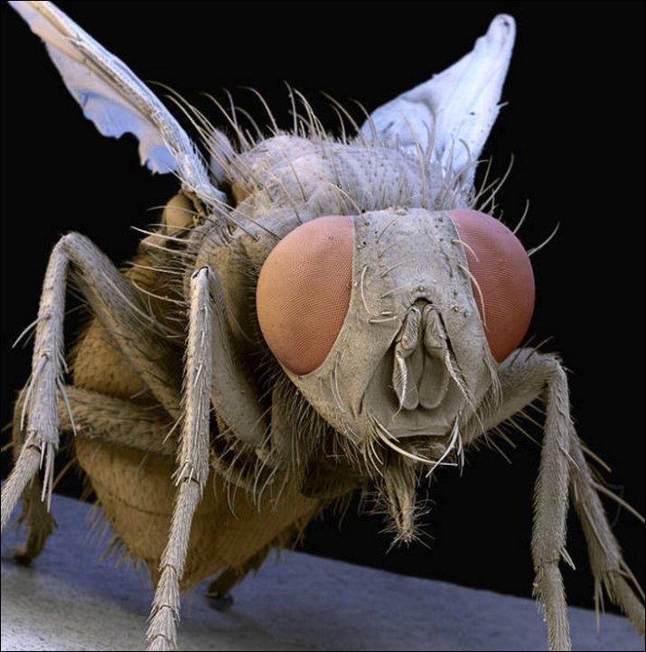
 Introduction to Scanning Electron Microscopy By: Brandon Cheney Ant s Leg Integrated Circuit Nano-composite This document was created as part of a Senior Project in the Materials Engineering Department
GBS765 Hybrid methods
 GBS765 Hybrid methods Lecture 3 Contrast and image formation 10/20/14 4:37 PM The lens ray diagram Magnification M = A/a = v/u and 1/u + 1/v = 1/f where f is the focal length The lens ray diagram So we
Oct. 30th- Nov. 1st, 2017
 Thomas LaGrange, Ph.D. Faculty Lecturer and Senior Staff Scientist Electron Sources, Optics and Detectors SEM Doctoral Course MS-636 Oct. 30th- Nov. 1st, 2017 Summary Electron propagation is only possible
Low Voltage Electron Microscope
 LVEM 25 Low Voltage Electron Microscope fast compact powerful Delong America FAST, COMPACT AND POWERFUL The LVEM 25 offers a high-contrast, high-throughput, and compact solution with nanometer resolutions.
LVEM 25. Low Voltage Electron Mictoscope. fast compact powerful
 LVEM 25 Low Voltage Electron Mictoscope fast compact powerful FAST, COMPACT AND POWERFUL The LVEM 25 offers a high-contrast, high-throughput, and compact solution with nanometer resolutions. All the benefits
Low Voltage Electron Microscope. Nanoscale from your benchtop LVEM5. Delong America
 LVEM5 Low Voltage Electron Microscope Nanoscale from your benchtop LVEM5 Delong America DELONG INSTRUMENTS COMPACT BUT POWERFUL The LVEM5 is designed to excel across a broad range of applications in material
Electron
 Electron 1897: Sir Joseph John Thomson (1856-1940) discovered corpuscles small particles with a charge-to-mass ratio over 1000 times greater than that of protons. Plum pudding model : electrons in a sea
Scanning Electron Microscopy
 Scanning Electron Microscopy For the semiconductor industry A tutorial Titel Vorname Nachname Titel Jobtitle, Bereich/Abteilung Overview Scanning Electron microscopy Scanning Electron Microscopy (SEM)
No part of this material may be reproduced without explicit written permission.
 This material is provided for educational use only. The information in these slides including all data, images and related materials are the property of : Robert M. Glaeser Department of Molecular & Cell
p q p f f f q f p q f NANO 703-Notes Chapter 5-Magnification and Electron Sources
 Chapter 5-agnification and Electron Sources Lens equation Let s first consider the properties of an ideal lens. We want rays diverging from a point on an object in front of the lens to converge to a corresponding
Lab 05: Transmission Electron Microscopy
 Lab 05: Transmission Electron Microscopy Author: Mike Nill Alex Bryant Contents 1 Introduction 2 1.1 Imaging Modes....................................... 2 1.2 Electromagnetic Lenses..................................
Fabrication of Probes for High Resolution Optical Microscopy
 Fabrication of Probes for High Resolution Optical Microscopy Physics 564 Applied Optics Professor Andrès La Rosa David Logan May 27, 2010 Abstract Near Field Scanning Optical Microscopy (NSOM) is a technique
Design and fabrication of a scanning electron microscope using a finite element analysis for electron optical system
 Journal of Mechanical Science and Technology 22 (2008) 1734~1746 Journal of Mechanical Science and Technology www.springerlink.com/content/1738-494x DOI 10.1007/s12206-008-0317-9 Design and fabrication
Introduction: Why electrons?
 Introduction: Why electrons? 1 Radiations Visible light X-rays Electrons Neutrons Advantages Not very damaging Easily focused Eye wonderful detector Small wavelength (Angstroms) Good penetration Small
Lecture 20: Optical Tools for MEMS Imaging
 MECH 466 Microelectromechanical Systems University of Victoria Dept. of Mechanical Engineering Lecture 20: Optical Tools for MEMS Imaging 1 Overview Optical Microscopes Video Microscopes Scanning Electron
Introduction of New Products
 Field Emission Electron Microscope JEM-3100F For evaluation of materials in the fields of nanoscience and nanomaterials science, TEM is required to provide resolution and analytical capabilities that can
Chapter Ray and Wave Optics
 109 Chapter Ray and Wave Optics 1. An astronomical telescope has a large aperture to [2002] reduce spherical aberration have high resolution increase span of observation have low dispersion. 2. If two
SECONDARY ELECTRON DETECTION
 SECONDARY ELECTRON DETECTION CAMTEC Workshop Presentation Haitian Xu June 14 th 2010 Introduction SEM Raster scan specimen surface with focused high energy e- beam Signal produced by beam interaction with
Recent results from the JEOL JEM-3000F FEGTEM in Oxford
 Recent results from the JEOL JEM-3000F FEGTEM in Oxford R.E. Dunin-Borkowski a, J. Sloan b, R.R. Meyer c, A.I. Kirkland c,d and J. L. Hutchison a a b c d Department of Materials, Parks Road, Oxford OX1
Observing Microorganisms through a Microscope LIGHT MICROSCOPY: This type of microscope uses visible light to observe specimens. Compound Light Micros
 PHARMACEUTICAL MICROBIOLOGY JIGAR SHAH INSTITUTE OF PHARMACY NIRMA UNIVERSITY Observing Microorganisms through a Microscope LIGHT MICROSCOPY: This type of microscope uses visible light to observe specimens.
PROCEEDINGS OF A SYMPOSIUM HELD AT THE CAVENDISH LABORATORY, CAMBRIDGE, Edited by
 X - R A Y M I C R O S C O P Y A N D M I C R O R A D I O G R A P H Y PROCEEDINGS OF A SYMPOSIUM HELD AT THE CAVENDISH LABORATORY, CAMBRIDGE, 1956 Edited by V. E. COSSLETT Cavendish Laboratory, University
5. The Scanning Electron Microscope
 Physical Principles of Electron Microscopy 5. The Scanning Electron Microscope Ray Egerton University of Alberta and National Institute of Nanotechnology Edmonton, Canada www.tem-eels.ca regerton@ualberta.ca
Low-energy Electron Diffractive Imaging for Three dimensional Light-element Materials
 Low-energy Electron Diffractive Imaging for Three dimensional Light-element Materials Hitachi Review Vol. 61 (2012), No. 6 269 Osamu Kamimura, Ph. D. Takashi Dobashi OVERVIEW: Hitachi has been developing
Functions of the SEM subsystems
 Functions of the SEM subsystems Electronic column It consists of an electron gun and two or more electron lenses, which influence the path of electrons traveling down an evacuated tube. The base of the
A Portable Scanning Electron Microscope Column Design Based on the Use of Permanent Magnets
 SCANNING VOL. 20, 87 91 (1998) Received October 8, 1997 FAMS, Inc. Accepted with revision November 9, 1997 A Portable Scanning Electron Microscope Column Design Based on the Use of Permanent Magnets A.
Applications of Optics
 Nicholas J. Giordano www.cengage.com/physics/giordano Chapter 26 Applications of Optics Marilyn Akins, PhD Broome Community College Applications of Optics Many devices are based on the principles of optics
Confocal Imaging Through Scattering Media with a Volume Holographic Filter
 Confocal Imaging Through Scattering Media with a Volume Holographic Filter Michal Balberg +, George Barbastathis*, Sergio Fantini % and David J. Brady University of Illinois at Urbana-Champaign, Urbana,
Tecnai on-line help manual --
 Tecnai on-line help Alignments 1 Tecnai on-line help manual -- Alignments Table of Contents 1 Alignments in the Tecnai microscope...5 2 Alignment procedures...6 3 Introduction to electron optics...11 3.1
TSBB09 Image Sensors 2018-HT2. Image Formation Part 1
 TSBB09 Image Sensors 2018-HT2 Image Formation Part 1 Basic physics Electromagnetic radiation consists of electromagnetic waves With energy That propagate through space The waves consist of transversal
CS-TEM vs CS-STEM. FEI Titan CIME EPFL. Duncan Alexander EPFL-CIME
 CS-TEM vs CS-STEM Duncan Alexander EPFL-CIME 1 FEI Titan Themis @ CIME EPFL 60 300 kv Monochromator High brightness X-FEG Probe Cs-corrected: 0.7 Å @ 300 kv Image Cs-corrected: 0.7 Å @ 300 kv Super-X EDX
Point Spread Function. Confocal Laser Scanning Microscopy. Confocal Aperture. Optical aberrations. Alternative Scanning Microscopy
 Bi177 Lecture 5 Adding the Third Dimension Wide-field Imaging Point Spread Function Deconvolution Confocal Laser Scanning Microscopy Confocal Aperture Optical aberrations Alternative Scanning Microscopy
Mirrors and Lenses. Images can be formed by reflection from mirrors. Images can be formed by refraction through lenses.
 Mirrors and Lenses Images can be formed by reflection from mirrors. Images can be formed by refraction through lenses. Notation for Mirrors and Lenses The object distance is the distance from the object
Heisenberg) relation applied to space and transverse wavevector
 relation applied to space and transverse wavevector") 2. Optical Microscopy 2.1 Principles A microscope is in principle nothing else than a simple lens system for magnifying small objects. The first lens, called the objective, has a short focal length (a
2. Optical Microscopy 2.1 Principles A microscope is in principle nothing else than a simple lens system for magnifying small objects. The first lens, called the objective, has a short focal length (a
PHYSICS. Chapter 35 Lecture FOR SCIENTISTS AND ENGINEERS A STRATEGIC APPROACH 4/E RANDALL D. KNIGHT
 PHYSICS FOR SCIENTISTS AND ENGINEERS A STRATEGIC APPROACH 4/E Chapter 35 Lecture RANDALL D. KNIGHT Chapter 35 Optical Instruments IN THIS CHAPTER, you will learn about some common optical instruments and
VISUAL PHYSICS ONLINE DEPTH STUDY: ELECTRON MICROSCOPES
 VISUAL PHYSICS ONLINE DEPTH STUDY: ELECTRON MICROSCOPES Shortly after the experimental confirmation of the wave properties of the electron, it was suggested that the electron could be used to examine objects
Microscopic Structures
 Microscopic Structures Image Analysis Metal, 3D Image (Red-Green) The microscopic methods range from dark field / bright field microscopy through polarisation- and inverse microscopy to techniques like
ECEN. Spectroscopy. Lab 8. copy. constituents HOMEWORK PR. Figure. 1. Layout of. of the
 ECEN 4606 Lab 8 Spectroscopy SUMMARY: ROBLEM 1: Pedrotti 3 12-10. In this lab, you will design, build and test an optical spectrum analyzer and use it for both absorption and emission spectroscopy. The
Exam 4. Name: Class: Date: Multiple Choice Identify the choice that best completes the statement or answers the question.
 Name: Class: Date: Exam 4 Multiple Choice Identify the choice that best completes the statement or answers the question. 1. Mirages are a result of which physical phenomena a. interference c. reflection
Mohammed A. Hussein *
 International Journal of Physics, 216, Vol. 4, No. 5, 13-134 Available online at http://pubs.sciepub.com/ijp/4/5/3 Science and Education Publishing DOI:1.12691/ijp-4-5-3 Effect of the Geometrical Shape
plasmonic nanoblock pair
 Nanostructured potential of optical trapping using a plasmonic nanoblock pair Yoshito Tanaka, Shogo Kaneda and Keiji Sasaki* Research Institute for Electronic Science, Hokkaido University, Sapporo 1-2,
Full-screen mode Popup controls. Overview of the microscope user interface, TEM User Interface and TIA on the left and EDS on the right
 Quick Guide to Operating FEI Titan Themis G2 200 (S)TEM: TEM mode Susheng Tan Nanoscale Fabrication and Characterization Facility, University of Pittsburgh Office: M104/B01 Benedum Hall, 412-383-5978,
First Results from a Retarding Field Angle-Resolved Analyzer
 First Results from a Retarding Field Angle-Resolved Analyzer J. Antel Jr., G. R. Harp Department of Physics and Astronomy Ohio University Athens, OH 45701 USA A LEED-like display analyzer is discussed.
Numerical analysis to verifying the performance of condenser magnetic lens in the scanning electron microscope.
 Numerical analysis to verifying the performance of condenser magnetic lens in the scanning electron microscope. Mohammed Abdullah Hussein Dept. of mechanization and agricultural equipment, College of agriculture
A Parallel Radial Mirror Energy Analyzer Attachment for the Scanning Electron Microscope
 142 doi:10.1017/s1431927615013288 Microscopy Society of America 2015 A Parallel Radial Mirror Energy Analyzer Attachment for the Scanning Electron Microscope Kang Hao Cheong, Weiding Han, Anjam Khursheed
Spectroscopy of Ruby Fluorescence Physics Advanced Physics Lab - Summer 2018 Don Heiman, Northeastern University, 1/12/2018
 1 Spectroscopy of Ruby Fluorescence Physics 3600 - Advanced Physics Lab - Summer 2018 Don Heiman, Northeastern University, 1/12/2018 I. INTRODUCTION The laser was invented in May 1960 by Theodor Maiman.
Resolution. Diffraction from apertures limits resolution. Rayleigh criterion θ Rayleigh = 1.22 λ/d 1 peak at 2 nd minimum. θ f D
 Microscopy Outline 1. Resolution and Simple Optical Microscope 2. Contrast enhancement: Dark field, Fluorescence (Chelsea & Peter), Phase Contrast, DIC 3. Newer Methods: Scanning Tunneling microscopy (STM),
Reflection! Reflection and Virtual Image!
 1/30/14 Reflection - wave hits non-absorptive surface surface of a smooth water pool - incident vs. reflected wave law of reflection - concept for all electromagnetic waves - wave theory: reflected back
THE BOTTOM LINE I. THE MICROSCOPE
 THE BOTTOM LINE This document is designed to help students focus their attention on basic concepts that are important for understanding the fundamental principles of transmission electron microscopy, biological
Measurement of Microscopic Three-dimensional Profiles with High Accuracy and Simple Operation
 238 Hitachi Review Vol. 65 (2016), No. 7 Featured Articles Measurement of Microscopic Three-dimensional Profiles with High Accuracy and Simple Operation AFM5500M Scanning Probe Microscope Satoshi Hasumura
CS-TEM vs CS-STEM. FEI Titan CIME EPFL. Duncan Alexander EPFL-CIME
 CS-TEM vs CS-STEM Duncan Alexander EPFL-CIME 1 FEI Titan Themis @ CIME EPFL 60 300 kv Monochromator High brightness X-FEG Probe Cs-corrected: 0.7 Å @ 300 kv Image Cs-corrected: 0.7 Å @ 300 kv Super-X EDX
Medical Imaging. X-rays, CT/CAT scans, Ultrasound, Magnetic Resonance Imaging
 Medical Imaging X-rays, CT/CAT scans, Ultrasound, Magnetic Resonance Imaging From: Physics for the IB Diploma Coursebook 6th Edition by Tsokos, Hoeben and Headlee And Higher Level Physics 2 nd Edition
Applied Optics. , Physics Department (Room #36-401) , ,
 , ,") Applied Optics Professor, Physics Department (Room #36-401) 2290-0923, 019-539-0923, shsong@hanyang.ac.kr Office Hours Mondays 15:00-16:30, Wednesdays 15:00-16:30 TA (Ph.D. student, Room #36-415) 2290-0921,
Applied Optics Professor, Physics Department (Room #36-401) 2290-0923, 019-539-0923, shsong@hanyang.ac.kr Office Hours Mondays 15:00-16:30, Wednesdays 15:00-16:30 TA (Ph.D. student, Room #36-415) 2290-0921,
Image Formation. Light from distant things. Geometrical optics. Pinhole camera. Chapter 36
 Light from distant things Chapter 36 We learn about a distant thing from the light it generates or redirects. The lenses in our eyes create images of objects our brains can process. This chapter concerns
Filter & Spectrometer Electron Optics
 Filter & Spectrometer Electron Optics Parameters Affecting Practical Performance Daniel Moonen & Harold A. Brink Did Something Go Wrong? 30 20 10 0 500 600 700 800 900 1000 1100 ev 1 Content The Prism
Imaging Systems Laboratory II. Laboratory 8: The Michelson Interferometer / Diffraction April 30 & May 02, 2002
 1051-232 Imaging Systems Laboratory II Laboratory 8: The Michelson Interferometer / Diffraction April 30 & May 02, 2002 Abstract. In the last lab, you saw that coherent light from two different locations
Microscope anatomy, image formation and resolution
 Microscope anatomy, image formation and resolution Ian Dobbie Buy this book for your lab: D.B. Murphy, "Fundamentals of light microscopy and electronic imaging", ISBN 0-471-25391-X Visit these websites:
The Nature of Light. Light and Energy
 The Nature of Light Light and Energy - dependent on energy from the sun, directly and indirectly - solar energy intimately associated with existence of life -light absorption: dissipate as heat emitted
Waveguiding in PMMA photonic crystals
 ROMANIAN JOURNAL OF INFORMATION SCIENCE AND TECHNOLOGY Volume 12, Number 3, 2009, 308 316 Waveguiding in PMMA photonic crystals Daniela DRAGOMAN 1, Adrian DINESCU 2, Raluca MÜLLER2, Cristian KUSKO 2, Alex.
EE119 Introduction to Optical Engineering Spring 2002 Final Exam. Name:
 EE119 Introduction to Optical Engineering Spring 2002 Final Exam Name: SID: CLOSED BOOK. FOUR 8 1/2 X 11 SHEETS OF NOTES, AND SCIENTIFIC POCKET CALCULATOR PERMITTED. TIME ALLOTTED: 180 MINUTES Fundamental
Physics 3340 Spring Fourier Optics
 Physics 3340 Spring 011 Purpose Fourier Optics In this experiment we will show how the Fraunhofer diffraction pattern or spatial Fourier transform of an object can be observed within an optical system.
Cs-corrector. Felix de Haas
 Cs-corrector. Felix de Haas Content Non corrector systems Lens aberrations and how to minimize? Corrector systems How is it done? Lens aberrations Spherical aberration Astigmatism Coma Chromatic Quality
BMB/Bi/Ch 173 Winter 2018
 BMB/Bi/Ch 73 Winter 208 Homework Set 2 (200 Points) Assigned -7-8, due -23-8 by 0:30 a.m. TA: Rachael Kuintzle. Office hours: SFL 229, Friday /9 4:00-5:00pm and SFL 220, Monday /22 4:00-5:30pm. For the
X-rays in medical diagnostics
 X-rays in medical diagnostics S.Dolanski Babić 2017/18. History W.C.Röntgen (1845-1923) discovered a new type of radiation Nature, Jan. 23. 1896.; Science, Feb.14. 1896. X- rays: Induced the ionization
The Resolution in the Electron Microscopy
 Volume 3, Issue, February 1 ISSN 319-87 The Resolution in the Electron Microscopy ABSTRACT Benefit from the group's equations, especially the resolution limits in the transmission electron microscope (TEM)