CS-TEM vs CS-STEM. FEI Titan CIME EPFL. Duncan Alexander EPFL-CIME
|
|
|
- Margery Kelly
- 6 years ago
- Views:
Transcription

1 CS-TEM vs CS-STEM Duncan Alexander EPFL-CIME 1 FEI Titan CIME EPFL kv Monochromator High brightness X-FEG Probe Cs-corrected: kv Image Cs-corrected: kv Super-X EDX detector GIF Quantum ERS energy filter Dual-channel, Ultrafast STEM-EELS Lorentz mode Biprism for holography Piezo stage Tomographic acquisition 2

 No CS With CS Resolution in HR-TEM")
 Combination of standard radially-symmetric")

2 Limitation to spatial resolution: aberrations Electromagnetic lenses in TEM column are toroidal Lenses inherently convergent => spherical aberration (CS) and chromatic aberration (CC) No CS With CS Resolution in HR-TEM limited by aberrations, especially CS 3 Cs-correction (STEM and TEM) Combination of standard radially-symmetric convergent lenses! with multipole divergent lenses (e.g. tetrapoles, hextapoles) to tune CS CEOS corrector Rose J. Electron Microscopy! 58 (2009)
3 Principle of aberration correction Compensate CS and other distortions with equivalent but opposite components to add together with aim of giving ideal spherical wavefront Krivanek et al. Aberration Correction in Electron Microscopy, Handbook of Charged Particle Physics 2009, pp CEOS aberration corrector CEOS aberration corrector used for imaging correction in CTEM also used before sample as probe-corrector for STEM; sextapole-round lens-sextapole design. This is an indirect corrector type; ~30 power supplies but higher power and water cooling needed. Krivanek et al. Aberration Correction in Electron Microscopy, Handbook of Charged Particle Physics 2009, pp

4 Nion aberration corrector First STEM aberration corrector installed on VG by Nion (Krivanek); quadrupoleoctopole design. This is a direct-action corrector type as now used on Nion UltraSTEM: ~70 power supplies needed but low power and which can fit onto printed circuit boards Krivanek et al. Aberration Correction in Electron Microscopy, Handbook of Charged Particle Physics 2009, pp Current correctors CEOS: CS-corrected, C5 optimised : CETCOR, CESCOR, D-COR CEOS: CS-CC corrected (NCEM TEAM 1.0, Julich Titan Pico) CEOS: B-COR aplanatic optimised for far off-axis rays JEOL: unique CS-CC corrector (CCC project) JEOL: Dodecapole Cs corrector ( Grand ARM ) Nion: CS-C5 corrected 8
, sample drift, Stobbs factor For CS-STEM need to understand concepts of: Probe size,")
stabilities, detectors 9 Cs-corrected HR-TEM interferometry Example:!")
5 Understanding resolution in EM For CS-TEM need to understand concepts of: Contrast transfer function (CTF) How to use CS to optimise CTF Difference between point resolution and information limit Properties of the camera (MTF), sample drift, Stobbs factor For CS-STEM need to understand concepts of: Probe size, shape, brightness, depth of field (DOF) Optical transfer function (OTF); STEM first to achieve 0.5 " res Scan (in)stabilities, detectors 9 Cs-corrected HR-TEM interferometry Example:!3 grain boundaries in Al Uncorrected CS-corrected Images: Oikawa, JEOL Image of projected potential Reduced delocalisation in phase contrast image 10
6 CTF curves: uncorrected microscopes 200 kv Talos: - Cs: 1.2 mm - Scherzer defocus: 65.8 nm - Point resolution: 2.4 Å - Information limit: 1.2 Å Here under focus defined as positive defocus value (as in JEMS) 300 kv Talos : - Cs: 1.2 mm - Scherzer defocus: 58.3 nm - Point resolution: 2.0 Å - Information limit: 1.2 Å 300 kv CM300 UT: - Cs: 0.7 mm - Scherzer defocus: 44.7 nm - Point resolution: 1.8 Å - Information limit: 1.2 Å Negative phase of CTF black atom contrast (as in JEMS) 11 Cs-TEM: effect on CTF 300 kv Titan: - Cs: 10 μm (adjustable!) - Defocus: -4.4 nm - Point resolution: ~0.7 Å - Information limit: 0.7 Å Higher information limit from shifting spatial and temporal envelopes Done by improved stability of instrument + monochromatic beam Here show negative Cs ( white atom contrast) Adjust Cs, defocus to give one wide CTF pass band to information limit 12
as nanowire Sample courtesy of Yannick Fontana, Anna Fontcuberta-i-Morral, LMSC 14")
7 Cs-TEM example: (AlxGa1 x)as nanowire Sample courtesy of Yannick Fontana, Anna Fontcuberta-i-Morral, LMSC 13 Cs-TEM example: (AlxGa1 x)as nanowire Sample courtesy of Yannick Fontana, Anna Fontcuberta-i-Morral, LMSC 14
![Cs-TEM [1 1 0] GaAs simulation Thickness: +1.6 nm steps from +3.](/docs-images/75/72913698/images/8-0.jpg "2 nm Defocus: 2 nm steps starting from +5 nm 15 Cs-TEM: defocus effect on CTF 300 kv Titan: - Cs: 10 μm (adjustable!")

8 Cs-TEM [1 1 0] GaAs simulation Thickness: +1.6 nm steps from +3.2 nm Defocus: 2 nm steps starting from +5 nm 15 Cs-TEM: defocus effect on CTF 300 kv Titan: - Cs: 10 μm (adjustable!) - Defocus: -4.4 nm - Point resolution: ~0.7 Å - Information limit: 0.7 Å Small change in defocus large change in contrast of high spatial frequencies! 300 kv Titan: - Cs: 10 μm (adjustable!) - Defocus: -0.4 nm - Information limit: 0.7 Å 300 kv Titan: - Cs: 10 μm (adjustable!) - Defocus: 3.6 nm - Information limit: 0.7 Å 16
as nanowire")


9 Cs-STEM example: (AlxGa1 x)as nanowire HAADF imaging: directly interpretable contrast on! atomic structure; camera-like focus and no delocalisation! 17 Benefits of aberration correction 18

")


TEM")

")
: imaging of")

10 Analytics STEM-EELS Atomic resolution core-loss STEM-EELS mapping (Nion UltraSTEM) More recently: atomic resolution EDX, EFTEM! but are they as interpretable? 19 Imaging organic molecules Cs-(S)TEM Cs-TEM (80 kev beam): imaging of molecule as weak phase object Lee et al. Nano Letters 9 (2009) Cs-STEM (200 kev beam): imaging of molecules by HAADF;! need very clean (un-contaminating) sample Gunawan et al. Chem. Mater 26 (2014)

11 Measurement precision CS-TEM 21 Measurement precision CS-STEM 22
 suffer knock-on damage.")


12 The move to lower kv Before CS-correction highest resolution by minimising $ (MeV instruments with $ < 1 pm) Light materials (graphene, nanotubes, ) suffer knock-on damage. Some thresholds: Bulk graphene: 86 kev Graphene edge atom: 36 kev Therefore need low kv 80 kv max but 60 kv better!which have long wavelengths Aberration correction now mandatory for atomic resolution Notable projects: Suenaga CCC project (30 kv aim), Ute Kaiser s Salve project (20 kv aim), both with combined CS-CC correctors; new UltraSTEM ( kv range) 23 Doped graphene, BN monolayer CS-STEM Analysis of monolayer materials: low kv essential to prevent knock-on damage; here 60 kv used (knock-on threshold for bulk graphene ~86 kv) with Nion UltraSTEM Medium-angle ADF (MAADF) gives intensity I! Z 1.7 but with increased signal intensity compared to true HAADF image. (This intensity is needed for imaging single atom by single atom; % = mrad.) Direct atom assignment by intensity. Krivanek et al Nature 464 (2010)


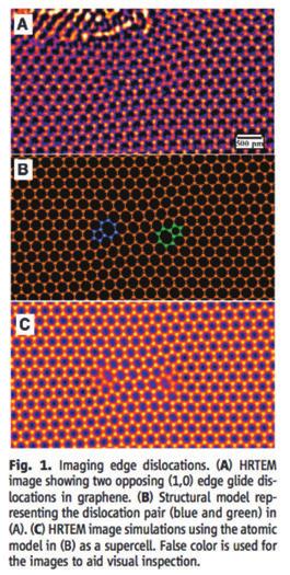
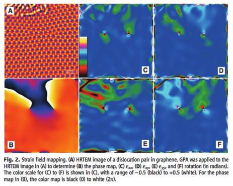
13 Doped graphene, BN monolayer CS-TEM 25 CS-TEM of dislocations in graphene 26


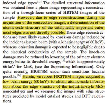
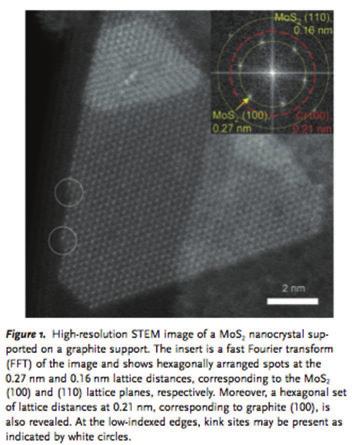
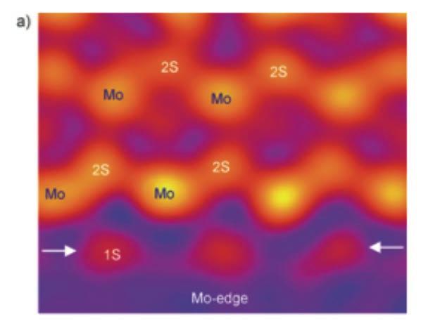
14 Studies of monolayer MoS2 2010: Cs-TEM, 80 kv, TEAM 0.5 microscope 27 Studies of monolayer MoS2 2011: Cs-STEM, 60 kv, SuperSTEM 28


15 Titan Themis Cs-STEM: CVD monolayer MoS2 Large-area MoS2 grown using H2S as the sulphur source! Dumitru Dumcenco et al. 2D Materials 2(4) nm 80 kev beam; even if below knock-on threshold can have beam-induced chemistry with residual gas molecules in column because not UHV (e.g. water etching). UHV or sample heating can be essential to good work! 29 Other limits 30
16 CS-TEM Harder to align precisely on zone axis (need to flip from diffraction to image) Interpret via: focal series reconstruction; negative Cs imaging; simulation Easy to obtain fringe image but precise Scherzer focus potentially challenging Contrast inversions with thickness remain; but can image very thick samples Damage: beam intensity spread, but total dose may be higher Coherent imaging: CTF determines resolution limit Atomic column analytics with (CCcorrected) EFTEM less proven Camera properties important (MTF, Stobbs factor ) Picometer measurement precision Dynamics studies 25 fps easy, 1000 fps now possible (good for ETEM) Can still image samples which contaminate, e.g. organic molecules CS-STEM Easier to align precisely on zone axis (always in diffraction mode) Interpret via HAADF/MAADF/BF/ABF/ idpc image Very limited DOF but very precise focus; camera-like focus Arguably thickness insensitive: sample first nms of thickness Damage: strong local intensity, but total dose may be lower Incoherent imaging: OTF determines resolution limit for HAADF Atomic column analytics with STEM- EELS; STEM-EDX also works Scan instabilities and detector noise important; need very stable scan Equally good precision Slower, but possible to follow movement of single atoms Need contamination-free samples only UHV possibility 31
CS-TEM vs CS-STEM. FEI Titan CIME EPFL. Duncan Alexander EPFL-CIME
 CS-TEM vs CS-STEM Duncan Alexander EPFL-CIME 1 FEI Titan Themis @ CIME EPFL 60 300 kv Monochromator High brightness X-FEG Probe Cs-corrected: 0.7 Å @ 300 kv Image Cs-corrected: 0.7 Å @ 300 kv Super-X EDX
Nanotechnology in Consumer Products
 Nanotechnology in Consumer Products Advances in Transmission Electron Microscopy Friday, April 21, 2017 October 31, 2014 The webinar will begin at 1pm Eastern Time Click here to watch the webinar recording
High Resolution Transmission Electron Microscopy (HRTEM) Summary 4/11/2018. Thomas LaGrange Faculty Lecturer and Senior Staff Scientist
 Summary 4/11/2018. Thomas LaGrange Faculty Lecturer and Senior Staff Scientist") Thomas LaGrange Faculty Lecturer and Senior Staff Scientist High Resolution Transmission Electron Microscopy (HRTEM) Doctoral Course MS-637 April 16-18th, 2018 Summary Contrast in TEM images results from
Thomas LaGrange Faculty Lecturer and Senior Staff Scientist High Resolution Transmission Electron Microscopy (HRTEM) Doctoral Course MS-637 April 16-18th, 2018 Summary Contrast in TEM images results from
Cs-corrector. Felix de Haas
 Cs-corrector. Felix de Haas Content Non corrector systems Lens aberrations and how to minimize? Corrector systems How is it done? Lens aberrations Spherical aberration Astigmatism Coma Chromatic Quality
Chapter 1. Basic Electron Optics (Lecture 2)
") Chapter 1. Basic Electron Optics (Lecture 2) Basic concepts of microscope (Cont ) Fundamental properties of electrons Electron Scattering Instrumentation Basic conceptions of microscope (Cont ) Ray diagram
Chapter 1. Basic Electron Optics (Lecture 2) Basic concepts of microscope (Cont ) Fundamental properties of electrons Electron Scattering Instrumentation Basic conceptions of microscope (Cont ) Ray diagram
High-resolution imaging on C s -corrected Titan
 High-resolution imaging on C s -corrected Titan 80-300 A new era for new results In NanoResearch a detailed knowledge of the structure of the material down to the atomic level is crucial for understanding
JEM-F200. Multi-purpose Electron Microscope. Scientific / Metrology Instruments Multi-purpose Electron Microscope
 Scientific / Metrology Instruments Multi-purpose Electron Microscope JEM-F200 Multi-purpose Electron Microscope JEM-F200/F2 is a multi-purpose electron microscope of the new generation to meet today's
Recent results from the JEOL JEM-3000F FEGTEM in Oxford
 Recent results from the JEOL JEM-3000F FEGTEM in Oxford R.E. Dunin-Borkowski a, J. Sloan b, R.R. Meyer c, A.I. Kirkland c,d and J. L. Hutchison a a b c d Department of Materials, Parks Road, Oxford OX1
Electron Sources, Optics and Detectors
 Thomas LaGrange, Ph.D. Faculty Lecturer and Senior Staff Scientist Electron Sources, Optics and Detectors TEM Doctoral Course MS-637 April 16 th -18 th, 2018 Summary Electron propagation is only possible
Transmission Electron Microscopy 9. The Instrument. Outline
 Transmission Electron Microscopy 9. The Instrument EMA 6518 Spring 2009 02/25/09 Outline The Illumination System The Objective Lens and Stage Forming Diffraction Patterns and Images Alignment and Stigmation
Introduction to Transmission Electron Microscopy (Physical Sciences)
") Introduction to Transmission Electron Microscopy (Physical Sciences) Centre for Advanced Microscopy Program 9:30 10:45 Lecture 1 Basics of TEM 10:45 11:00 Morning tea 11:00 12:15 Lecture 2 Diffraction
Introduction to Transmission Electron Microscopy (Physical Sciences) Centre for Advanced Microscopy Program 9:30 10:45 Lecture 1 Basics of TEM 10:45 11:00 Morning tea 11:00 12:15 Lecture 2 Diffraction
The application of spherical aberration correction and focal series restoration to high-resolution images of platinum nanocatalyst particles
 Journal of Physics: Conference Series The application of spherical aberration correction and focal series restoration to high-resolution images of platinum nanocatalyst particles Recent citations - Miguel
Introduction to Electron Microscopy-II
 Introduction to Electron Microscopy-II Prof. David Muller, dm24@cornell.edu Rm 274 Clark Hall, 255-4065 Ernst Ruska and Max Knoll built the first electron microscope in 1931 (Nobel Prize to Ruska in 1986)
Aberration corrected tilt series restoration
 Journal of Physics: Conference Series Aberration corrected tilt series restoration To cite this article: S Haigh et al 2008 J. Phys.: Conf. Ser. 126 012042 Recent citations - Artefacts in geometric phase
NanoSpective, Inc Progress Drive Suite 137 Orlando, Florida
 TEM Techniques Summary The TEM is an analytical instrument in which a thin membrane (typically < 100nm) is placed in the path of an energetic and highly coherent beam of electrons. Typical operating voltages
2.Components of an electron microscope. a) vacuum systems, b) electron guns, c) electron optics, d) detectors. Marco Cantoni 021/
 vacuum systems, b) electron guns, c) electron optics, d) detectors. Marco Cantoni 021/") 2.Components of an electron microscope a) vacuum systems, b) electron guns, c) electron optics, d) detectors, 021/693.48.16 Centre Interdisciplinaire de Microscopie Electronique CIME Summary Electron propagation
2.Components of an electron microscope a) vacuum systems, b) electron guns, c) electron optics, d) detectors, 021/693.48.16 Centre Interdisciplinaire de Microscopie Electronique CIME Summary Electron propagation
Chapter 2 Instrumentation for Analytical Electron Microscopy Lecture 7. Chapter 2 CHEM Fall L. Ma
 Chapter 2 Instrumentation for Analytical Electron Microscopy Lecture 7 Outline Electron Sources (Electron Guns) Thermionic: LaB 6 or W Field emission gun: cold or Schottky Lenses Focusing Aberration Probe
TEM theory Basic optics, image formation and key elements
 Workshop series of Chinese 3DEM community Get acquainted with Cryo-Electron Microscopy: First Chinese Workshop for Structural Biologists TEM theory Basic optics, image formation and key elements Jianlin
Atomic-Level Control of the Thermoelectric Properties in Polytypoid Nanowires
 Atomic-Level Control of the Thermoelectric Properties in Polytypoid Nanowires Sean C. Andrews 1,2 *, Melissa A. Fardy 1,2 *, Michael C. Moore 1,2 *, Shaul Aloni 2, Minjuan Zhang 3, Velimir Radmilovic 2,4,
Scanning Transmission Electron Microscopy for Nanostructure Characterization
 6 Scanning Transmission Electron Microscopy for Nanostructure Characterization S. J. Pennycook, A. R. Lupini, M. Varela, A. Y. Borisevich, Y. Peng, M. P. Oxley, K. van Benthem, M. F. Chisholm 1. Introduction
Introduction to Electron Microscopy
 Introduction to Electron Microscopy Prof. David Muller, dm24@cornell.edu Rm 274 Clark Hall, 255-4065 Ernst Ruska and Max Knoll built the first electron microscope in 1931 (Nobel Prize to Ruska in 1986)
Supplementary Figure 1. 2-Fold astigmatism. (a-f) Multi-slice image simulations of graphene structure with variation of the level of 2-fold
 Multi-slice image simulations of graphene structure with variation of the level of 2-fold") Supplementary Figure 1. 2-Fold astigmatism. (a-f) Multi-slice image simulations of graphene structure with variation of the level of 2-fold astigmatism increasing from 0 to 1.0 nm with an interval of 0.2nm.
Supplementary Figure 1. 2-Fold astigmatism. (a-f) Multi-slice image simulations of graphene structure with variation of the level of 2-fold astigmatism increasing from 0 to 1.0 nm with an interval of 0.2nm.
2014 HTD-E with options
 with options The HT7700 : a user-friendly, ergonomic digital TEM with options User-Friendly r end Design Ambient light operation. Multiple automated functions for alignment, focus and stigmation as standard
No part of this material may be reproduced without explicit written permission.
 This material is provided for educational use only. The information in these slides including all data, images and related materials are the property of : Robert M. Glaeser Department of Molecular & Cell
Electron
 Electron 1897: Sir Joseph John Thomson (1856-1940) discovered corpuscles small particles with a charge-to-mass ratio over 1000 times greater than that of protons. Plum pudding model : electrons in a sea
Tutorial on Linear Image Simulations of Phase-Contrast and Incoherent Imaging by convolutions
 Tutorial on Linear Image Simulations of Phase-Contrast and Incoherent Imaging by convolutions Huolin Xin, David Muller, based on Appendix A of Kirkland s book This tutorial covers the use of temcon and
2.Components of an electron microscope. a) vacuum systems, b) electron guns, c) electron optics, d) detectors. Marco Cantoni, 021/
 vacuum systems, b) electron guns, c) electron optics, d) detectors. Marco Cantoni, 021/") 2.Components of an electron microscope a) vacuum systems, b) electron guns, c) electron optics, d) detectors Marco Cantoni, 021/693.48.16 Centre Interdisciplinaire de Microscopie Electronique CIME MSE-603
2.Components of an electron microscope a) vacuum systems, b) electron guns, c) electron optics, d) detectors Marco Cantoni, 021/693.48.16 Centre Interdisciplinaire de Microscopie Electronique CIME MSE-603
Quantitative HRTEM investigation of an obtuse angle dislocation reaction in gold with a C S corrected field emission microscope
 Quantitative HRTEM investigation of an obtuse angle dislocation reaction in gold with a C S corrected field emission microscope Joerg R. Jinschek 1, Ch. Kisielowski 1,2, T. Radetic 1, U. Dahmen 1, M. Lentzen
Phase plates for cryo-em
 Max Planck Institute of Biochemistry Martinsried, Germany MAX PLANCK SOCIETY Phase plates for cryo-em Rado Danev Max Planck Institute of Biochemistry, Martinsried, Germany. EMBO course 2017, London, UK
Advanced Materials Characterization Workshop
 University of Illinois at Urbana-Champaign Materials Research Laboratory Advanced Materials Characterization Workshop June 3 rd and 4 th, 2013 Transmission Electron Microscopy Wacek Swiech, Honghui Zhou,
Contrast transfer. Contrast transfer and CTF correction. Lecture 6 H Saibil
 Lecture 6 H Saibil Contrast transfer Contrast transfer and CTF correction The weak phase approximation Contrast transfer function Determining defocus CTF correction methods Image processing for cryo microscopy
A Tutorial on Electron Microscopy
 A Tutorial on Electron Microscopy Jian-Min (Jim) Zuo Mat. Sci. Eng. and Seitz-Materials Research Lab., UIUC Outline of This Tutorial I. Science and opportunities of electron microscopy II. The basic TEM,
Introduction of New Products
 Field Emission Electron Microscope JEM-3100F For evaluation of materials in the fields of nanoscience and nanomaterials science, TEM is required to provide resolution and analytical capabilities that can
Low-energy Electron Diffractive Imaging for Three dimensional Light-element Materials
 Low-energy Electron Diffractive Imaging for Three dimensional Light-element Materials Hitachi Review Vol. 61 (2012), No. 6 269 Osamu Kamimura, Ph. D. Takashi Dobashi OVERVIEW: Hitachi has been developing
Indiana University JEM-3200FS
 Indiana University JEM-3200FS Installation Specification Model: JEM 3200FS Serial Number: EM 15000013 Objective Lens Configuration: High Resolution Pole Piece (HRP) JEOL Engineer: Michael P. Van Etten
NANO 703-Notes. Chapter 9-The Instrument
 1 Chapter 9-The Instrument Illumination (condenser) system Before (above) the sample, the purpose of electron lenses is to form the beam/probe that will illuminate the sample. Our electron source is macroscopic
Appreciating the very little things: Status and future prospects of TEM at NUANCE
 Appreciating the very little things: Status and future prospects of TEM at NUANCE Dr. Roberto dos Reis roberto.reis@northwestern.edu 11/28/2018 Nature 542, pages75 79 (2017) TEM Facility Manager: Dr. Xiaobing
Full-screen mode Popup controls. Overview of the microscope user interface, TEM User Interface and TIA on the left and EDS on the right
 Quick Guide to Operating FEI Titan Themis G2 200 (S)TEM: TEM mode Susheng Tan Nanoscale Fabrication and Characterization Facility, University of Pittsburgh Office: M104/B01 Benedum Hall, 412-383-5978,
ELECTRON MICROSCOPY. 13:10 16:00, Oct. 6, 2008 Institute of Physics, Academia Sinica. Tung Hsu
 ELECTRON MICROSCOPY 13:10 16:00, Oct. 6, 2008 Institute of Physics, Academia Sinica Tung Hsu Department of Materials Science and Engineering National Tsing Hua University Hsinchu 300, TAIWAN Tel. 03-5742564
Scanning electron microscope
 Scanning electron microscope 6 th CEMM workshop Maja Koblar, Sc. Eng. Physics Outline The basic principle? What is an electron? Parts of the SEM Electron gun Electromagnetic lenses Apertures Chamber and
Development of JEM-2800 High Throughput Electron Microscope
 Development of JEM-2800 High Throughput Electron Microscope Mitsuhide Matsushita, Shuji Kawai, Takeshi Iwama, Katsuhiro Tanaka, Toshiko Kuba and Noriaki Endo EM Business Unit, JEOL Ltd. Electron Optics
Transmissions Electron Microscopy (TEM)
") Transmissions Electron Microscopy (TEM) Basic principles Diffraction Imaging Specimen preparation A.E. Gunnæs MENA3100 V17 TEM is based on three possible set of techniqes Diffraction From regions down
Transmissions Electron Microscopy (TEM) Basic principles Diffraction Imaging Specimen preparation A.E. Gunnæs MENA3100 V17 TEM is based on three possible set of techniqes Diffraction From regions down
MASSACHUSETTS INSTITUTE OF TECHNOLOGY. 2.71/2.710 Optics Spring 14 Practice Problems Posted May 11, 2014
 MASSACHUSETTS INSTITUTE OF TECHNOLOGY 2.71/2.710 Optics Spring 14 Practice Problems Posted May 11, 2014 1. (Pedrotti 13-21) A glass plate is sprayed with uniform opaque particles. When a distant point
Progress in aberration-corrected scanning transmission electron microscopy
 Japanese Society of Electron Microscopy Journal of Electron Microscopy 50(3): 177 185 (2001)... Full-length paper Progress in aberration-corrected scanning transmission electron microscopy Niklas Dellby,
Criteria for Optical Systems: Optical Path Difference How do we determine the quality of a lens system? Several criteria used in optical design
 Criteria for Optical Systems: Optical Path Difference How do we determine the quality of a lens system? Several criteria used in optical design Computer Aided Design Several CAD tools use Ray Tracing (see
Nanotechnology and material science Lecture V
 Most widely used nanoscale microscopy. Based on possibility to create bright electron beam with sub-nm spot size. History: Ernst Ruska (1931), Nobel Prize (1986) For visible light λ=400-700nm, for electrons
GBS765 Hybrid methods
 GBS765 Hybrid methods Lecture 3 Contrast and image formation 10/20/14 4:37 PM The lens ray diagram Magnification M = A/a = v/u and 1/u + 1/v = 1/f where f is the focal length The lens ray diagram So we
Paul Mooney Gatan, Inc. October 31, 2017
 Paul Mooney Gatan, Inc. October 31, 2017 Leverage Detection Algo Image formation Resolution (Å) Electron-counting cryo-electron microscopy* 4 3.5 3 2.5 *Hong Zhou in: Science, 6/30/2017 and J. General
A research on the development of the resolution improvement methods in electron microscopy , China.
 4th International Conference on Computer, Mechatronics, Control and Electronic Engineering (ICCMCEE 2015) A research on the development of the resolution improvement methods in electron microscopy Nana
Low Voltage Electron Microscope
 LVEM5 Low Voltage Electron Microscope Nanoscale from your benchtop LVEM5 Delong America DELONG INSTRUMENTS COMPACT BUT POWERFUL The LVEM5 is designed to excel across a broad range of applications in material
Low Voltage Electron Microscope
 LVEM 25 Low Voltage Electron Microscope fast compact powerful Delong America FAST, COMPACT AND POWERFUL The LVEM 25 offers a high-contrast, high-throughput, and compact solution with nanometer resolutions.
Atomic Resolution Imaging with a sub-50 pm Electron Probe
 Atomic Resolution Imaging with a sub-50 pm Electron Probe Rolf Erni, Marta D. Rossell, Christian Kisielowski, Ulrich Dahmen National Center for Electron Microscopy, Lawrence Berkeley National Laboratory
LVEM 25. Low Voltage Electron Mictoscope. fast compact powerful
 LVEM 25 Low Voltage Electron Mictoscope fast compact powerful FAST, COMPACT AND POWERFUL The LVEM 25 offers a high-contrast, high-throughput, and compact solution with nanometer resolutions. All the benefits
Cover Page. The handle holds various files of this Leiden University dissertation.
 Cover Page The handle http://hdl.handle.net/1887/2083 holds various files of this Leiden University dissertation. Author: Schramm, Sebastian Markus Title: Imaging with aberration-corrected low energy electron
Aberrations and adaptive optics for biomedical microscopes
 Aberrations and adaptive optics for biomedical microscopes Martin Booth Department of Engineering Science And Centre for Neural Circuits and Behaviour University of Oxford Outline Rays, wave fronts and
Chapter Ray and Wave Optics
 109 Chapter Ray and Wave Optics 1. An astronomical telescope has a large aperture to [2002] reduce spherical aberration have high resolution increase span of observation have low dispersion. 2. If two
Scanning electron microscope
 Scanning electron microscope 5 th CEMM workshop Maja Koblar, Sc. Eng. Physics Outline The basic principle? What is an electron? Parts of the SEM Electron gun Electromagnetic lenses Apertures Detectors
Image Contrast Theory
 Image Contrast Theory Wah Chiu wah@bcm.tmc.edu National Center for Macromolecular Imaging References Jiang, W. & Chiu, W. Web-based simulation for contrast transfer function and envelope functions. Microsc
1.1. In regular TEM imaging mode, find a region of interest and set it at eucentric height.
 JEOL 2010F operating procedure Covers operation in STEM mode (See separate procedures for operation in TEM mode and operation of EDS system) Nicholas G. Rudawski ngr@ufl.edu (805) 252-4916 NOTE: this operating
Chapter 4 Imaging Lecture 17
 Chapter 4 Imaging Lecture 17 d (110) Imaging Imaging in the TEM Diffraction Contrast in TEM Image HRTEM (High Resolution Transmission Electron Microscopy) Imaging STEM imaging Imaging in the TEM What is
S200 Course LECTURE 1 TEM
 S200 Course LECTURE 1 TEM Development of Electron Microscopy 1897 Discovery of the electron (J.J. Thompson) 1924 Particle and wave theory (L. de Broglie) 1926 Electromagnetic Lens (H. Busch) 1932 Construction
BMB/Bi/Ch 173 Winter 2018
 BMB/Bi/Ch 73 Winter 208 Homework Set 2 (200 Points) Assigned -7-8, due -23-8 by 0:30 a.m. TA: Rachael Kuintzle. Office hours: SFL 229, Friday /9 4:00-5:00pm and SFL 220, Monday /22 4:00-5:30pm. For the
Low Voltage Electron Microscope. Nanoscale from your benchtop LVEM5. Delong America
 LVEM5 Low Voltage Electron Microscope Nanoscale from your benchtop LVEM5 Delong America DELONG INSTRUMENTS COMPACT BUT POWERFUL The LVEM5 is designed to excel across a broad range of applications in material
--> Buy True-PDF --> Auto-delivered in 0~10 minutes. JY/T
 Translated English of Chinese Standard: JY/T011-1996 www.chinesestandard.net Sales@ChineseStandard.net INDUSTRY STANDARD OF THE JY PEOPLE S REPUBLIC OF CHINA General rules for transmission electron microscopy
STEM Spectrum Imaging Tutorial
 STEM Spectrum Imaging Tutorial Gatan, Inc. 5933 Coronado Lane, Pleasanton, CA 94588 Tel: (925) 463-0200 Fax: (925) 463-0204 April 2001 Contents 1 Introduction 1.1 What is Spectrum Imaging? 2 Hardware 3
This document assumes the user is already familiar with basic operation of the instrument in TEM mode and use of the Microscope Control interface.
 FEI Tecnai F20 S/TEM: imaging in STEM mode Nicholas G. Rudawski ngr@ufl.edu (805) 252-4916 (352) 392-3077 Last updated: 05/10/18 This document assumes the user is already familiar with basic operation
WIEN Software for Design of Columns Containing Wien Filters and Multipole Lenses
 WIEN Software for Design of Columns Containing Wien Filters and Multipole Lenses An integrated workplace for analysing and optimising the column optics Base Package (WIEN) Handles round lenses, quadrupoles,
Optics and Lasers. Matt Young. Including Fibers and Optical Waveguides
 Matt Young Optics and Lasers Including Fibers and Optical Waveguides Fourth Revised Edition With 188 Figures Springer-Verlag Berlin Heidelberg New York London Paris Tokyo Hong Kong Barcelona Budapest Contents
Transmission electron Microscopy
 Transmission electron Microscopy Image formation of a concave lens in geometrical optics Some basic features of the transmission electron microscope (TEM) can be understood from by analogy with the operation
ELECTRON MICROSCOPY. 09:10 12:00, Oct. 27, 2006 Institute of Physics, Academia Sinica. Tung Hsu
 ELECTRON MICROSCOPY 09:10 12:00, Oct. 27, 2006 Institute of Physics, Academia Sinica Tung Hsu Department of Materials Science and Engineering National Tsinghua University Hsinchu 300, TAIWAN Tel. 03-5742564
Yuta Sato, Kazu Suenaga, Shingo Okubo, Toshiya Okazaki, and Sumio Iijima
 The Structures of D 5d -C 80 and I h -Er 3 N@C 80 Fullerenes and their Rotation inside Carbon Nanotubes demonstrated by Aberration-Corrected Electron Microscopy Yuta Sato, Kazu Suenaga, Shingo Okubo, Toshiya
CHAPTER TWO METALLOGRAPHY & MICROSCOPY
 CHAPTER TWO METALLOGRAPHY & MICROSCOPY 1. INTRODUCTION: Materials characterisation has two main aspects: Accurately measuring the physical, mechanical and chemical properties of materials Accurately measuring
ELECTRON MICROSCOPY AN OVERVIEW
 ELECTRON MICROSCOPY AN OVERVIEW Anjali Priya 1, Abhishek Singh 2, Nikhil Anand Srivastava 3 1,2,3 Department of Electrical & Instrumentation, Sant Longowal Institute of Engg. & Technology, Sangrur, India.
Mirrors, Lenses &Imaging Systems
 Mirrors, Lenses &Imaging Systems We describe the path of light as straight-line rays And light rays from a very distant point arrive parallel 145 Phys 24.1 Mirrors Standing away from a plane mirror shows
How to choose the optimal microscope/camera combinations
 How to choose the optimal microscope/camera combinations The Practical Matters Anchi Cheng National Resource for Automated Common Mistakes I have money; I will get everything, regardless. I don t have
STEM alignment procedures
 STEM alignment procedures Step 1. ASID alignment mode 1. Write down STD for TEM, and then open the ASID control window from dialogue. Also, start Simple imager viewer program on the Desktop. 2. Click on
Optical Engineering 421/521 Sample Questions for Midterm 1
 Optical Engineering 421/521 Sample Questions for Midterm 1 Short answer 1.) Sketch a pechan prism. Name a possible application of this prism., write the mirror matrix for this prism (or any other common
Confocal Imaging Through Scattering Media with a Volume Holographic Filter
 Confocal Imaging Through Scattering Media with a Volume Holographic Filter Michal Balberg +, George Barbastathis*, Sergio Fantini % and David J. Brady University of Illinois at Urbana-Champaign, Urbana,
J. C. Wyant Fall, 2012 Optics Optical Testing and Testing Instrumentation
 J. C. Wyant Fall, 2012 Optics 513 - Optical Testing and Testing Instrumentation Introduction 1. Measurement of Paraxial Properties of Optical Systems 1.1 Thin Lenses 1.1.1 Measurements Based on Image Equation
Chapter 1. Introduction
 Chapter 1 Introduction 1.1 Where are the Atoms? Uncovering objects that are too small to be seen by eye: this is the primary purpose of microscopy. The human eye enables us to resolve objects that are
Filter & Spectrometer Electron Optics
 Filter & Spectrometer Electron Optics Parameters Affecting Practical Performance Daniel Moonen & Harold A. Brink Did Something Go Wrong? 30 20 10 0 500 600 700 800 900 1000 1100 ev 1 Content The Prism
ABC Math Student Copy. N. May ABC Math Student Copy. Physics Week 13(Sem. 2) Name. Light Chapter Summary Cont d 2
 Name. Light Chapter Summary Cont d 2") Page 1 of 12 Physics Week 13(Sem. 2) Name Light Chapter Summary Cont d 2 Lens Abberation Lenses can have two types of abberation, spherical and chromic. Abberation occurs when the rays forming an image
Page 1 of 12 Physics Week 13(Sem. 2) Name Light Chapter Summary Cont d 2 Lens Abberation Lenses can have two types of abberation, spherical and chromic. Abberation occurs when the rays forming an image
EE119 Introduction to Optical Engineering Spring 2003 Final Exam. Name:
 EE119 Introduction to Optical Engineering Spring 2003 Final Exam Name: SID: CLOSED BOOK. THREE 8 1/2 X 11 SHEETS OF NOTES, AND SCIENTIFIC POCKET CALCULATOR PERMITTED. TIME ALLOTTED: 180 MINUTES Fundamental
Exam 4. Name: Class: Date: Multiple Choice Identify the choice that best completes the statement or answers the question.
 Name: Class: Date: Exam 4 Multiple Choice Identify the choice that best completes the statement or answers the question. 1. Mirages are a result of which physical phenomena a. interference c. reflection
Characterisation of a novel super-polished bimorph mirror
 Characterisation of a novel super-polished bimorph mirror Kawal Sawhney 1, Simon Alcock 1, Hongchang Wang 1, John Sutter 1 and Riccardo Signorato 2 1 Diamond Light Source Ltd. UK 2 BASC, D-51429 Bergisch
Optical Information Processing. Adolf W. Lohmann. Edited by Stefan Sinzinger. Ch>
 Optical Information Processing Adolf W. Lohmann Edited by Stefan Sinzinger Ch> Universitätsverlag Ilmenau 2006 Contents Preface to the 2006 edition 13 Preface to the third edition 15 Preface volume 1 17
FYS 4340/FYS Diffraction Methods & Electron Microscopy. Lecture 9. Imaging Part I. Sandeep Gorantla. FYS 4340/9340 course Autumn
 FYS 4340/FYS 9340 Diffraction Methods & Electron Microscopy Lecture 9 Imaging Part I Sandeep Gorantla FYS 4340/9340 course Autumn 2016 1 Imaging 2 Abbe s principle of imaging Unlike with visible light,
*Corresponding author.
 Supporting Information for: Ligand-Free, Quantum-Confined Cs 2 SnI 6 Perovskite Nanocrystals Dmitriy S. Dolzhnikov, Chen Wang, Yadong Xu, Mercouri G. Kanatzidis, and Emily A. Weiss * Department of Chemistry,
Optimisation. Lecture 3
 Optimisation Lecture 3 Objectives: Lecture 3 At the end of this lecture you should: 1. Understand the use of Petzval curvature to balance lens components 2. Know how different aberrations depend on field
Software for Electron and Ion Beam Column Design. An integrated workplace for simulating and optimizing electron and ion beam columns
 OPTICS Software for Electron and Ion Beam Column Design An integrated workplace for simulating and optimizing electron and ion beam columns Base Package (OPTICS) Field computation Imaging and paraxial
A few concepts in TEM and STEM explained
 A few concepts in TEM and STEM explained Martin Ek November 23, 2011 1 Introduction This is a collection of short, qualitative explanations of key concepts in TEM and STEM. Most of them are beyond what
Fabrication of Probes for High Resolution Optical Microscopy
 Fabrication of Probes for High Resolution Optical Microscopy Physics 564 Applied Optics Professor Andrès La Rosa David Logan May 27, 2010 Abstract Near Field Scanning Optical Microscopy (NSOM) is a technique
TSBB09 Image Sensors 2018-HT2. Image Formation Part 1
 TSBB09 Image Sensors 2018-HT2 Image Formation Part 1 Basic physics Electromagnetic radiation consists of electromagnetic waves With energy That propagate through space The waves consist of transversal
Converging and Diverging Surfaces. Lenses. Converging Surface
 Lenses Sandy Skoglund 2 Converging and Diverging s AIR Converging If the surface is convex, it is a converging surface in the sense that the parallel rays bend toward each other after passing through the
Modulation Transfer Function
 Modulation Transfer Function The Modulation Transfer Function (MTF) is a useful tool in system evaluation. t describes if, and how well, different spatial frequencies are transferred from object to image.
Lecture 21. Physics 1202: Lecture 21 Today s Agenda
 Physics 1202: Lecture 21 Today s Agenda Announcements: Team problems today Team 14: Gregory Desautels, Benjamin Hallisey, Kyle Mcginnis Team 15: Austin Dion, Nicholas Gandza, Paul Macgillis-Falcon Homework
Chapter 17: Wave Optics. What is Light? The Models of Light 1/11/13
 Chapter 17: Wave Optics Key Terms Wave model Ray model Diffraction Refraction Fringe spacing Diffraction grating Thin-film interference What is Light? Light is the chameleon of the physical world. Under
Towards accurate measurements with synchrotron tomography Problems and pitfalls. Robert C. Atwood. Nghia T. Vo, Michael Drakopoulos, Thomas Connolley
 Towards accurate measurements with synchrotron tomography Problems and pitfalls Robert C. Atwood Nghia T. Vo, Michael Drakopoulos, Thomas Connolley Artefacts in Synchrotron X-ray Tomography Rings Rings
Microscope anatomy, image formation and resolution
 Microscope anatomy, image formation and resolution Ian Dobbie Buy this book for your lab: D.B. Murphy, "Fundamentals of light microscopy and electronic imaging", ISBN 0-471-25391-X Visit these websites: