Topics 3b,c Electron Microscopy
|
|
|
- Cecilia Wilcox
- 6 years ago
- Views:
Transcription
1 Topics 3b,c Electron Microscopy 1.0 Introduction and History 1.1 Characteristic Information 2.0 Basic Principles 2.1 Electron-Solid Interactions 2.2 Electromagnetic Lenses 2.3 Breakdown of an Electron Microscope 2.4 Signal Detection and Display 2.5 Operating Parameters 3.0 Instrumentation 3.1 Sample Prep 4.0 Artifacts and Examples 5.0 Summary 1.0 Introduction and History o Electron microscopes are scientific instruments that use a beam of energetic electrons to examine objects on a very fine scale. o Electron microscopes were developed due to the limitations of Light Microscopes which are limited by the physics of light. o In the early 1930's this theoretical limit had been reached and there was a scientific desire to see the fine details of the interior structures of organic cells (nucleus, mitochondria...etc.). o This required 10,000x plus magnification which was not possible using current optical microscopes.
2 Comparison of OM,TEM and SEM Light source Condenser Eyepiece Specimen Objective Projector Source of electrons Magnetic lenses Specimen (Cathode Ray Tube) CRT Image Viewed Directly Light Microscope Image on Fluorescent Screen Transmission Electron Microscope detector Scanning Electron Microscope Principal features of an optical microscope, a transmission electron microscope and a scanning electron microscope, drawn to emphasize the similarities of overall design. University of Tennessee, Dept. of Materials Science and Engineering 3 Dates The transmission electron microscope (TEM) was the first type of Electron Microscope to be developed and is patterned exactly on the light transmission microscope except that a focused beam of electrons is used instead of light to "see through" the specimen. It was developed by Max Knoll and Ernst Ruska in Germany in The first scanning electron microscope (SEM) debuted in 1938 ( Von Ardenne) with the first commercial instruments around Its late development was due to the electronics involved in "scanning" the beam of electrons across the sample.

3 1.1 Characteristic Information: SEM Topography The surface features of an object or "how it looks", its texture; direct relation between these features and materials properties Morphology The shape and size of the particles making up the object; direct relation between these structures and materials properties Composition The elements and compounds that the object is composed of and the relative amounts of them; direct relationship between composition and materials properties Crystallographic Information How the atoms are arranged in the object; direct relation between these arrangements and material properties e.g. Identification of Fracture Mode Cracks Pores Grain boundary Cracks 4µm 20µm SEM micrographs of fractured surface of two BaTiO 3 samples.


4 OM vs. SEM 2D 3D 5 µm How Fine can You See? Can you see a sugar cube? The thickness of a sewing needle? The thickness of a piece of paper? The resolution of human eyes is of the order of 0.1 mm, 100µm 4 mils. However, something vital to human beings are of sizes smaller than 0.1mm, e.g. our cells, bacteria, microstructural details of materials, etc.
5 Microstructural Features which Concern Us Grain size: from <µm to the cm regime Grain shapes Precipitate size: mostly in the µm regime Volume fractions and distributions of various phases Defects such as cracks and voids: <µm to the cm regime Scale and Microscopy Techniques XRD,TEM SEM OM Crystal Structure Microstructure Component Grain I Valve Turbo charge Grain II Structure Determination Fracture Mechanics atomic Basic Research Applied Research Microstructure ranging from crystal structure to engine components (Si 3 N 4 )
6 Advantages of Using SEM over OM Mag Depth of Field Resolution OM: 4x 1400x 0.5mm ~ 0.2mm SEM: 10x 500Kx 30mm 1.5nm The SEM has a large depth of field, which allows a large amount of the sample to be in focus at one time and produces an image that is a good representation of the three-dimensional sample. The combination of higher magnification, larger depth of field, greater resolution, compositional and crystallographic information makes the SEM one of the most heavily used instruments in academic/national lab research areas and industry. 2.1 Electron-Solid Interactions When an electron beam strikes a sample, a large number of signals are generated. Incident e - Beam Backscattered e - Foil (TEM)Bulk (SEM) Auger e - Interaction Volume X-rays Inelastically Scattered e - Unscattered e - Cathodaluminescence Secondary e - Sample Elastically Scattered e - Transmitted Electrons We can divide the signals into two broad categories: a) electron signals, b) photon signals
7 Specimen Interaction Volume The volume inside the specimen in which interactions occur while interacting with an electron beam. This volume depends on the following factors: Atomic number of the material being examined; higher atomic number materials absorb or stop more electrons, smaller interaction volume. Accelerating voltage: higher voltages penetrate farther into the sample and generate a larger interaction volume Angle of incidence for the electron beam; the greater the angle (further from normal) the smaller the interaction volume. Specimen Interaction Volume Below is an example of a typical Interaction volume for: Specimen with atomic number 28, 20 kv 0 degrees tilt, incident beam is normal to specimen surface noting the approximate maximum sampling depths for the various interactions. Electron Beam Secondaries 100Å Augers 10Å to 30Å Backscattered <1-2µm 5 µm Range of K X-rays Range of L X-rays Range of Electron Penetration


8 5000 Å Beam Interaction Simulations Theoretical SrS density: 3.7g/cm 3, Long. range: 1062 Å, Long. straggle: 384 Å SrS Si 5000 Å SrS Si 10 kv 2 µm 15 kv 1 µm 5000 Å 5 kv SrS Si 2 kv SrS 2 µm 5000 Å University of Tennessee, Dept. of Materials Science and Engineering 0.5 µm 15 Electron Detectors and Sample Stage Objective lens Sample stage Example
9 2.2 Electromagnetic Lenses Lorentz force equation: F = q 0 v x B Two components to the B field: B L = longitudinal component (down the axis) B R = radial component (perpendicular to axis) Nonaxial electrons will experience a force both down the axis and one radial to it. Only electrons traveling down the axis feel equal radial forces from all sides of the lens. The unequal force felt by the off-axis electrons causes spiraling about the optic axis. after "Electron Beam Analysis of Materials", M.H. Loretto Electromagnetic Lenses The Condenser Lens For example with a thermionic gun, the diameter of the first cross-over point ~20-50µm. If we want to focus the beam to a size < 10 nm on the specimen surface, the magnification should be ~1/5000, which is not easily attained with one lens (say, the objective lens) only. Therefore, condenser lenses are added to demagnify the cross-over points.
10 Electromagnetic Lenses The Objective Lens The objective lens controls the final focus of the electron beam by changing the magnetic field strength The cross-over image is finally demagnified to a ~ 10nm beam spot which carries a beam current of approximately A. Scanning Coils Stigmator Beam-Limiting Aperture Electromagnetic Lenses The Objective Lens - Focusing By changing the current in the objective lens, the magnetic field strength changes and therefore the focal length of the objective lens is changed. Objective lens Out of focus lens current too strong In focus lens current optimized Out of focus lens current too weak
11 Electromagnetic Lenses The Objective Lens - Stigmator The objective lens is machined to very high precision and the magnetic field pattern is very carefully designed. However, the precision attainable by machining cannot match that required for controlling a beam with a 10 nm diameter. The stigmator, which consist of two pairs of pole-pieces arranged in the X and Y directions, is added to correct the minor imperfections in the objective lens. Electromagnetic Lenses The Objective Lens - Aperture Since the electrons coming from the electron gun have spread in kinetic energies and directions of movement, they may not be focused to the same plane to form a sharp spot. By inserting an aperture, the stray electrons are blocked and the remaining narrow beam will come to a narrow Disc of Least Confusion Electron beam Large beam diameter striking specimen Wide aperture Objective lens Wide disc of least confusion Narrow aperture Small beam diameter striking specimen Narrow disc of least confusion

12 Electron vs. Optical Lenses e - s don t actually touch the lens No definite interface e - s rotate in the magnetic field e - s repel each other f H I - Focus and magnification controlled electronically - No physical movements e - lenses can only be positive elements (converging) Can t correct e - lens aberrations like you can with compound optical lenses e - lenses always operate at small apertures H = MFS 2.3 Breakdown of an Electron Microscope Filament TV Screen Detector Electromagnets Stage Sample In simplest terms, an SEM is really nothing more than a television. We use a filament to get electrons, magnets to move them around, and a detector acts like a camera to produce an image.
13 Scanning Electron Microscope Virtual Source First Condenser Lens Condenser Aperture Second Condenser Lens Scan Coils Objective Aperture Objective Lens Sample 1) 2) 1) The "Virtual Source" at the top represents the electron gun, producing a stream of monochromatic electrons. 2) The stream is condensed by the first condenser lens (usually controlled by the "coarse probe current knob"). This lens is used to both form the beam and limit the amount of current in the beam. It works in conjunction with the condenser aperture to eliminate the high-angle electrons from the beam. Scanning Electron Microscope Virtual Source First Condenser Lens Condenser Aperture Second Condenser Lens Objective Aperture Scan Coils Objective Lens Sample 3) 4) 5) 3) The beam is then constricted by the condenser aperture (usually not user selectable), eliminating some high-angle electrons. 4) The second condenser lens forms the electrons into a thin, tight, coherent beam and is usually controlled by the "fine probe current knob". 5) A user selectable objective aperture further eliminates high-angle electrons from the beam. University of Tennessee, Dept. of Materials Science and Engineering 26
14 6) 7) 8) Scanning Electron Microscope Virtual Source First Condenser Lens Condenser Aperture Second Condenser Lens Objective Aperture Scan Coils Objective Lens Sample 6) A set of coils then "scan" or "sweep" the beam in a grid fashion (like a television), dwelling on points for a period of time determined by the scan speed (usually in the microsecond range). 7) The final lens, the objective, focuses the scanning beam onto the part of the specimen desired. 8) When the beam strikes the sample (and dwells for a few microseconds) interactions occur inside the sample and are detected with various instruments. University of Tennessee, Dept. of Materials Science and Engineering 27 Scanning Electron Microscope Virtual Source First Condenser Lens Condenser Aperture Second Condenser Lens Scan Coils Objective Aperture 9) Before the beam moves to its next dwell point these instruments count the number of e - interactions and display a pixel on a CRT whose intensity is determined by this number (the more reactions the brighter the pixel). Objective Lens Sample 10) This process is repeated until the grid scan is finished and then repeated, the entire pattern can be scanned 30 times/sec.

15 A Look Inside the Column Electron gun Gun Alignment Control Pneumatic Air Lock Valve Condenser Lens Objective Aperture Scanning Coil Objective Lens Motorized Stage Sample Chamber Summary of Electron Microscope Components 1. Electron optical column consists of: electron source to produce electrons magnetic lenses to de-magnify the beam magnetic coils to control and modify the beam apertures to define the beam, prevent electron spray, etc. 2. Vacuum systems consists of: chamber which holds vacuum, pumps to produce vacuum valves to control vacuum, gauges to monitor vacuum 3. Signal Detection & Display consists of: detectors which collect the signal electronics which produce an image from the signal
 Thermionic or Cold Cathode (Field Emission")
 The electric field at the tip is very strong (> 10 7 V/cm) due to the sharp point effect")
 is needed to avoid ion bombardment to the tip from the residual gas.")
16 Electron Beam Source Single Crystal LaB6 Heating Cup Heating Wire (W or Re) Support Posts Lanthanum Hexaboride Single Crystal Filament W / LaB 6 (Filament) Thermionic or Cold Cathode (Field Emission Gun) Field Emission Gun The tip of a tungsten needle is made very sharp (radius < 0.1 µm) The electric field at the tip is very strong (> 10 7 V/cm) due to the sharp point effect Electrons are pulled out from the tip by the strong electric field Ultra-high vacuum (better than 7.5 x 10⁻⁹ Torr - 6 x 10⁻⁶ Pa) is needed to avoid ion bombardment to the tip from the residual gas. Electron probe diameter < 1 nm is possible
17 2.4 Signal Detection and Display If you change the target material, the high and low energy peaks remain (although their intensity may change) while the low intensity peaks change position and are characteristic of the sample. The reason we produce this type of profile is because the incident electrons we send into the sample are scattered in different ways. There are two broad categories to describe electron scattering: elastic: Backscattered electrons inelastic: Secondary electrons Electron Detectors Objective lens Example
18 Secondary Electrons These electrons arise due to inelastic collisions between primary electrons (the beam) and loosely bound electrons of the conduction band (more probable) or tightly bound valence electrons. The energy transferred is sufficient to overcome the work function which binds them to the solid and they are ejected. Incident e - Electron Orbitals The interaction is Coulombic in nature and the ejected electrons typically have 5-10 ev. 50 ev is an arbitrary cut-off below which they are said to be secondary electrons. Detection Remember, secondary electrons are low energy electrons. We can easily collect them by placing a positive voltage ( V) on the front of our detector. Since this lets us collect a large number of the secondaries (50-100%), we produce a 3D type of image of the sample with a large depth of field. The type of detector used is called a scintillator / photomultiplier tube.
19 Detection Sequence (1) Al coated Scintillator 6-12 kv Scintillator / Photomultiplier (2) (3) Light Guide (4) E field (5) Grid v Photons Photocathode emits electrons Dinodes multiply the number of electrons 1. Secondary electrons (SE) are accelerated to the front of the detector by a bias voltage of ev. 2. They are then accelerated to the scintillator by a bias of 6-12 kev, (10 KeV is normal). 3. Scintillator is doped plastic or glass covered with a fluorescent material (e.g. Europium). A thin (700Å) layer of Al covers it to prevent light from causing fluorescence. The 10keV potential allows the SE to get through the Al and fluoresce. Detection Sequence (1) Al coated Scintillator 6-12 kv Scintillator / Photomultiplier (2) (3) Light Guide (4) E field (5) Grid v Photons Photocathode emits electrons Dinodes multiply the number of electrons 4. The light photons travel down the tube (guide) to a photocathode which converts them into electrons 5. The electrons move through the detector, producing more electrons as they strike dinodes. An output electron pulse is then detected. University of Tennessee, Dept. of Materials Science and Engineering 38
20 Backscattered Electrons Backscattered electrons (BSE) arise due to elastic collisions between the incoming electron and the nucleus of the target atom (i.e. Rutherford scattering). Higher Z, more BSE emitted. e - Nucleus As the name implies, elastic scattering results in little (< 1 ev) or no change in energy of the scattered electrons, although there is a change in momentum (p). Since p = mv and the mass of the electron doesn t change, the direction of the velocity vector must change. The angle of scattering can range from 0 to 180. Detection Since BSE have high energies, they can t be pulled in like secondaries. If you placed a potential on a grid to attract them, you would also attract the incident beam!! The most common detector used is called a surface barrier detector. It sits above the sample, below the objective lens. BSE which strike it are detected. Top Contact Backscattered Electrons Si Polepiece Annular Backscattered Electron Detector Thin Au Layer Electron - Hole Production P - N Junction Base Contact Current Monitor in External Circuit
21 Detection Sequence Surface barrier detectors are solid state devices made up of semiconducting materials. A semiconducting material has a filled valence band and an empty conduction band- similar to ceramic materials. 1. When a BSE electron strikes the detector, electrons in the material move from valence to conduction band. 2. The electrons are now free to move in the conduction band or drop back into the valence band. 3. If a potential is applied, the e- and e+ can be separated, collected, and the current measured. The strength of the current is proportional to the number of BSE that hit the detector. (3) (2) (1) 2.5 Operating Parameters Magnification An image is obtained by taking the signal from the sample and transferring it to a CRT screen. By decreasing the size of the scanned area (from which we get the signal), magnification is produced. L l Scanned Area Information transferred Mag. Area 10x (1cm) 2 100x (1mm) 2 1Kx (100 µm) 2 10Kx (10 µm) 2 100Kx (1 µm) 2 1Mx (100 nm) 2 Console CRT Magnification is determined by taking the ratio of the lengths of the scans: Mag. = L/I
22 Resolution Resolution is the ability to resolve two closely spaced points. While you may have to be at a high magnification to see small features, resolution is NOT the same as magnification. One way to improve resolution is by reducing the size of the electron beam that strikes the sample: d min = 1.29C 1/4 s λ 3/4 [7.92 (it/j c )x ] 3/8 at low current: d min = 1.29C 1/4 s λ 3/4 J c = current density of the source, λ = electron wavelength C s = spherical aberration, i = current, T = temperature, Resolution We can also improve the resolution by: Increasing the strength of the condenser lens Decreasing the size of the objective aperture Decreasing the working distance (WD = the distance the sample is from the objective lens) University of Tennessee, Dept. of Materials Science and Engineering 44
23 Depth of Field (I) The height over which a sample can be clearly focused is called the Depth of Field. The SEM has a large depth of field which produces the images that appear 3-dimensional in nature. Depth of field is improved by: Longer working distance Smaller objective apertures Lower magnifications Depth of Field (II) A beam having a semi-angle of convergence α will converge from a radius r to a focus and diverge again in a vertical distance D. For small α : D = 2r / α In a current high-resolution CRT s (spot size =0.1 mm = 100 microns), the focusing becomes objectionable when two pixels are fully overlapped, where the pixel size on the specimen is 0.1/M mm, where M is the magnification, which gives us the practical expression for the depth of focus/field: DOF 0.2 / αm (mm) University of Tennessee, Dept. of Materials Science and Engineering 46
24 Depth of Field (III) The angle α is determined by: α = r/wd r = radius of the aperture used, and WD is the working distance of the aperture from the specimen. University of Tennessee, Dept. of Materials Science and Engineering 47 Depth of Field vs. Resolution Depth of field and resolution have a reciprocal relationship: Improving resolution in conventional SEM s leads to a smaller depth of field While increasing depth of field decreases resolution.useful for each particular sample.

25 3.0 Instrumentation JEOL 6700F Ultra High Resolution Scanning Electron Microscope 3.1 Sample Preparation Sample Coating Q: Why? A: Charging: Deflection of SE s Increased emission of SE s in cracks Periodic SE bursts Beam deflection Solutions: Sputter coating with C, Cr, or Au-Pd Carbon tape, carbon paint, In foil
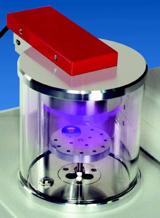
26 Sputtering Ion Beam Coating Gatan PECS Model #682


27 4.0 Artifacts and Examples Surface Etching Thermal damage - Sample temperature can rise up to 40 C Coating Film Adhesion: Not sticking, temperature sensitive Contamination Morphology Modification Stigmation Focus Depth of field Voltage Ag powders written by a laser on glass Ag powders written by a laser on glass Ag powders - Cerac, 190 nm average Ag powders - SMP, 400 nm average


28 Silica Spheres, 0.5 µm, Hereisus University of Tennessee, Dept. of Materials Science and Engineering 55 Native BS Compo Fe Alloy (Fe-Mo-Mn-Cr B) 5 PPA 50 PPA 500 PPA University of Tennessee, Dept. of Materials Science and Engineering 56


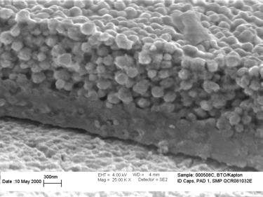
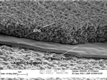
29 BTO and Ag powders written by a laser on Kapton University of Tennessee, Dept. of Materials Science and Engineering 57 BTO and Ag powders written by a laser on Kapton University of Tennessee, Dept. of Materials Science and Engineering 58


30 Space Shuttle Tile 100 µm University of Tennessee, Dept. 10 µm of Materials Science and Engineering µm University of Tennessee, Dept. of Materials Science and Engineering µm
31 5.0 Summary The basic layout and operation of an SEM. The different imaging modes of the SEM. How an image is obtained Sample preparation Materials Information: Imaging, composition (EDS, WDS, CL) Fabrication with EBL
Scanning electron microscope
 Scanning electron microscope 6 th CEMM workshop Maja Koblar, Sc. Eng. Physics Outline The basic principle? What is an electron? Parts of the SEM Electron gun Electromagnetic lenses Apertures Chamber and
Scanning electron microscope
 Scanning electron microscope 5 th CEMM workshop Maja Koblar, Sc. Eng. Physics Outline The basic principle? What is an electron? Parts of the SEM Electron gun Electromagnetic lenses Apertures Detectors
MODULE I SCANNING ELECTRON MICROSCOPE (SEM)
") MODULE I SCANNING ELECTRON MICROSCOPE (SEM) Scanning Electron Microscope (SEM) Initially, the plan of SEM was offered by H. Stintzing in 1927 (a German patent application). His suggested procedure was
MODULE I SCANNING ELECTRON MICROSCOPE (SEM) Scanning Electron Microscope (SEM) Initially, the plan of SEM was offered by H. Stintzing in 1927 (a German patent application). His suggested procedure was
S200 Course LECTURE 1 TEM
 S200 Course LECTURE 1 TEM Development of Electron Microscopy 1897 Discovery of the electron (J.J. Thompson) 1924 Particle and wave theory (L. de Broglie) 1926 Electromagnetic Lens (H. Busch) 1932 Construction
(Refer Slide Time: 00:10)
") Fundamentals of optical and scanning electron microscopy Dr. S. Sankaran Department of Metallurgical and Materials Engineering Indian Institute of Technology, Madras Module 03 Unit-6 Instrumental details
Fundamentals of optical and scanning electron microscopy Dr. S. Sankaran Department of Metallurgical and Materials Engineering Indian Institute of Technology, Madras Module 03 Unit-6 Instrumental details
Functions of the SEM subsystems
 Functions of the SEM subsystems Electronic column It consists of an electron gun and two or more electron lenses, which influence the path of electrons traveling down an evacuated tube. The base of the
p q p f f f q f p q f NANO 703-Notes Chapter 5-Magnification and Electron Sources
 Chapter 5-agnification and Electron Sources Lens equation Let s first consider the properties of an ideal lens. We want rays diverging from a point on an object in front of the lens to converge to a corresponding
Scanning Electron Microscopy Basics and Applications
 Scanning Electron Microscopy Basics and Applications Dr. Julia Deuschle Stuttgart Center for Electron Microscopy MPI for Solid State Research Room: 1E15, phone: 0711/ 689-1193 email: j.deuschle@fkf.mpg.de
ELECTRON MICROSCOPY AN OVERVIEW
 ELECTRON MICROSCOPY AN OVERVIEW Anjali Priya 1, Abhishek Singh 2, Nikhil Anand Srivastava 3 1,2,3 Department of Electrical & Instrumentation, Sant Longowal Institute of Engg. & Technology, Sangrur, India.
Introduction: Why electrons?
 Introduction: Why electrons? 1 Radiations Visible light X-rays Electrons Neutrons Advantages Not very damaging Easily focused Eye wonderful detector Small wavelength (Angstroms) Good penetration Small
Scanning Electron Microscopy. EMSE-515 F. Ernst
 Scanning Electron Microscopy EMSE-515 F. Ernst 1 2 Scanning Electron Microscopy Max Knoll Manfred von Ardenne Manfred von Ardenne Principle of Scanning Electron Microscopy 3 Principle of Scanning Electron
NANO 703-Notes. Chapter 9-The Instrument
 1 Chapter 9-The Instrument Illumination (condenser) system Before (above) the sample, the purpose of electron lenses is to form the beam/probe that will illuminate the sample. Our electron source is macroscopic
Scanning Electron Microscopy SEM. Warren Straszheim, PhD MARL, 23 Town Engineering
 Scanning Electron Microscopy SEM Warren Straszheim, PhD MARL, 23 Town Engineering wesaia@iastate.edu 515-294-8187 How it works Create a focused electron beam Accelerate it Scan it across the sample Map
Electron Sources, Optics and Detectors
 Thomas LaGrange, Ph.D. Faculty Lecturer and Senior Staff Scientist Electron Sources, Optics and Detectors TEM Doctoral Course MS-637 April 16 th -18 th, 2018 Summary Electron propagation is only possible
SCANNING ELECTRON MICROSCOPY AND X-RAY MICROANALYSIS
 SCANNING ELECTRON MICROSCOPY AND X-RAY MICROANALYSIS Robert Edward Lee Electron Microscopy Center Department of Anatomy and Neurobiology Colorado State University P T R Prentice Hall, Englewood Cliffs,
Scanning Electron Microscopy
 Scanning Electron Microscopy For the semiconductor industry A tutorial Titel Vorname Nachname Titel Jobtitle, Bereich/Abteilung Overview Scanning Electron microscopy Scanning Electron Microscopy (SEM)
SECONDARY ELECTRON DETECTION
 SECONDARY ELECTRON DETECTION CAMTEC Workshop Presentation Haitian Xu June 14 th 2010 Introduction SEM Raster scan specimen surface with focused high energy e- beam Signal produced by beam interaction with
2.Components of an electron microscope. a) vacuum systems, b) electron guns, c) electron optics, d) detectors. Marco Cantoni 021/
 vacuum systems, b) electron guns, c) electron optics, d) detectors. Marco Cantoni 021/") 2.Components of an electron microscope a) vacuum systems, b) electron guns, c) electron optics, d) detectors, 021/693.48.16 Centre Interdisciplinaire de Microscopie Electronique CIME Summary Electron propagation
2.Components of an electron microscope a) vacuum systems, b) electron guns, c) electron optics, d) detectors, 021/693.48.16 Centre Interdisciplinaire de Microscopie Electronique CIME Summary Electron propagation
Introduction of New Products
 Field Emission Electron Microscope JEM-3100F For evaluation of materials in the fields of nanoscience and nanomaterials science, TEM is required to provide resolution and analytical capabilities that can
NanoSpective, Inc Progress Drive Suite 137 Orlando, Florida
 TEM Techniques Summary The TEM is an analytical instrument in which a thin membrane (typically < 100nm) is placed in the path of an energetic and highly coherent beam of electrons. Typical operating voltages
Introduction to Scanning Electron Microscopy
 Introduction to Scanning Electron Microscopy By: Brandon Cheney Ant s Leg Integrated Circuit Nano-composite This document was created as part of a Senior Project in the Materials Engineering Department
ELECTRON MICROSCOPY. 13:10 16:00, Oct. 6, 2008 Institute of Physics, Academia Sinica. Tung Hsu
 ELECTRON MICROSCOPY 13:10 16:00, Oct. 6, 2008 Institute of Physics, Academia Sinica Tung Hsu Department of Materials Science and Engineering National Tsing Hua University Hsinchu 300, TAIWAN Tel. 03-5742564
Chapter 1. Basic Electron Optics (Lecture 2)
") Chapter 1. Basic Electron Optics (Lecture 2) Basic concepts of microscope (Cont ) Fundamental properties of electrons Electron Scattering Instrumentation Basic conceptions of microscope (Cont ) Ray diagram
Chapter 1. Basic Electron Optics (Lecture 2) Basic concepts of microscope (Cont ) Fundamental properties of electrons Electron Scattering Instrumentation Basic conceptions of microscope (Cont ) Ray diagram
2.Components of an electron microscope. a) vacuum systems, b) electron guns, c) electron optics, d) detectors. Marco Cantoni, 021/
 vacuum systems, b) electron guns, c) electron optics, d) detectors. Marco Cantoni, 021/") 2.Components of an electron microscope a) vacuum systems, b) electron guns, c) electron optics, d) detectors Marco Cantoni, 021/693.48.16 Centre Interdisciplinaire de Microscopie Electronique CIME MSE-603
2.Components of an electron microscope a) vacuum systems, b) electron guns, c) electron optics, d) detectors Marco Cantoni, 021/693.48.16 Centre Interdisciplinaire de Microscopie Electronique CIME MSE-603
Transmission electron Microscopy
 Transmission electron Microscopy Image formation of a concave lens in geometrical optics Some basic features of the transmission electron microscope (TEM) can be understood from by analogy with the operation
Applications of Optics
 Nicholas J. Giordano www.cengage.com/physics/giordano Chapter 26 Applications of Optics Marilyn Akins, PhD Broome Community College Applications of Optics Many devices are based on the principles of optics
Low Voltage Electron Microscope
 LVEM5 Low Voltage Electron Microscope Nanoscale from your benchtop LVEM5 Delong America DELONG INSTRUMENTS COMPACT BUT POWERFUL The LVEM5 is designed to excel across a broad range of applications in material
Introduction to Electron Microscopy
 Introduction to Electron Microscopy Prof. David Muller, dm24@cornell.edu Rm 274 Clark Hall, 255-4065 Ernst Ruska and Max Knoll built the first electron microscope in 1931 (Nobel Prize to Ruska in 1986)
CHAPTER TWO METALLOGRAPHY & MICROSCOPY
 CHAPTER TWO METALLOGRAPHY & MICROSCOPY 1. INTRODUCTION: Materials characterisation has two main aspects: Accurately measuring the physical, mechanical and chemical properties of materials Accurately measuring
ELECTRON MICROSCOPY. 14:10 17:00, Apr. 3, 2007 Department of Physics, National Taiwan University. Tung Hsu
 ELECTRON MICROSCOPY 14:10 17:00, Apr. 3, 2007 Department of Physics, National Taiwan University Tung Hsu Department of Materials Science and Engineering National Tsinghua University Hsinchu 300, TAIWAN
ZEISS EVO SOP. May 2017 ELECTRON OPTICS
 ZEISS EVO SOP May 2017 ELECTRON OPTICS The patented EVO column is the area of the SEM, where electrons are emitted, accelerated, deflected, focused, and scanned. Main characteristics of the EVO optics
Chapter 4 Imaging Lecture 17
 Chapter 4 Imaging Lecture 17 d (110) Imaging Imaging in the TEM Diffraction Contrast in TEM Image HRTEM (High Resolution Transmission Electron Microscopy) Imaging STEM imaging Imaging in the TEM What is
Observing Microorganisms through a Microscope LIGHT MICROSCOPY: This type of microscope uses visible light to observe specimens. Compound Light Micros
 PHARMACEUTICAL MICROBIOLOGY JIGAR SHAH INSTITUTE OF PHARMACY NIRMA UNIVERSITY Observing Microorganisms through a Microscope LIGHT MICROSCOPY: This type of microscope uses visible light to observe specimens.
Fabrication of Probes for High Resolution Optical Microscopy
 Fabrication of Probes for High Resolution Optical Microscopy Physics 564 Applied Optics Professor Andrès La Rosa David Logan May 27, 2010 Abstract Near Field Scanning Optical Microscopy (NSOM) is a technique
EE119 Introduction to Optical Engineering Fall 2009 Final Exam. Name:
 EE119 Introduction to Optical Engineering Fall 2009 Final Exam Name: SID: CLOSED BOOK. THREE 8 1/2 X 11 SHEETS OF NOTES, AND SCIENTIFIC POCKET CALCULATOR PERMITTED. TIME ALLOTTED: 180 MINUTES Fundamental
Introduction to Transmission Electron Microscopy (Physical Sciences)
") Introduction to Transmission Electron Microscopy (Physical Sciences) Centre for Advanced Microscopy Program 9:30 10:45 Lecture 1 Basics of TEM 10:45 11:00 Morning tea 11:00 12:15 Lecture 2 Diffraction
Introduction to Transmission Electron Microscopy (Physical Sciences) Centre for Advanced Microscopy Program 9:30 10:45 Lecture 1 Basics of TEM 10:45 11:00 Morning tea 11:00 12:15 Lecture 2 Diffraction
VISUAL PHYSICS ONLINE DEPTH STUDY: ELECTRON MICROSCOPES
 VISUAL PHYSICS ONLINE DEPTH STUDY: ELECTRON MICROSCOPES Shortly after the experimental confirmation of the wave properties of the electron, it was suggested that the electron could be used to examine objects
X-rays. X-rays are produced when electrons are accelerated and collide with a target. X-rays are sometimes characterized by the generating voltage
 X-rays Ouch! 1 X-rays X-rays are produced when electrons are accelerated and collide with a target Bremsstrahlung x-rays Characteristic x-rays X-rays are sometimes characterized by the generating voltage
Chapter 2 Instrumentation for Analytical Electron Microscopy Lecture 7. Chapter 2 CHEM Fall L. Ma
 Chapter 2 Instrumentation for Analytical Electron Microscopy Lecture 7 Outline Electron Sources (Electron Guns) Thermionic: LaB 6 or W Field emission gun: cold or Schottky Lenses Focusing Aberration Probe
OPERATION OF THE HITACHI S-450 SCANNING ELECTRON MICROSCOPE. by Doug Bray Department of Biological Sciences University of Lethbridge
 OPERATION OF THE HITACHI S-450 SCANNING ELECTRON MICROSCOPE by Doug Bray Department of Biological Sciences University of Lethbridge Revised September, 2000 Note: The terms in bold in this document represent
Oct. 30th- Nov. 1st, 2017
 Thomas LaGrange, Ph.D. Faculty Lecturer and Senior Staff Scientist Electron Sources, Optics and Detectors SEM Doctoral Course MS-636 Oct. 30th- Nov. 1st, 2017 Summary Electron propagation is only possible
Test Review # 8. Physics R: Form TR8.17A. Primary colors of light
 Physics R: Form TR8.17A TEST 8 REVIEW Name Date Period Test Review # 8 Light and Color. Color comes from light, an electromagnetic wave that travels in straight lines in all directions from a light source
Tecnai on-line help manual --
 Tecnai on-line help Alignments 1 Tecnai on-line help manual -- Alignments Table of Contents 1 Alignments in the Tecnai microscope...5 2 Alignment procedures...6 3 Introduction to electron optics...11 3.1
5. The Scanning Electron Microscope
 Physical Principles of Electron Microscopy 5. The Scanning Electron Microscope Ray Egerton University of Alberta and National Institute of Nanotechnology Edmonton, Canada www.tem-eels.ca regerton@ualberta.ca
Oct. 30th- Nov. 1st, 2017
 Thomas LaGrange, Ph.D. Faculty Lecturer and Senior Staff Scientist Electron Sources, Optics and Detectors SEM Doctoral Course MS-636 Oct. 30th- Nov. 1st, 2017 Summary Electron propagation is only possible
Test Review # 9. Physics R: Form TR9.15A. Primary colors of light
 Physics R: Form TR9.15A TEST 9 REVIEW Name Date Period Test Review # 9 Light and Color. Color comes from light, an electromagnetic wave that travels in straight lines in all directions from a light source
Operating the Hitachi 7100 Transmission Electron Microscope Electron Microscopy Core, University of Utah
 Operating the Hitachi 7100 Transmission Electron Microscope Electron Microscopy Core, University of Utah Follow the procedures below when you use the Hitachi 7100 TEM. Starting Session 1. Turn on the cold
Observing Microorganisms through a Microscope
 2016/2/19 PowerPoint Lecture Presentations prepared by Bradley W. Christian, McLennan Community College CHAPTER 3 Observing Microorganisms through a Microscope 1 Figure 3.2 Microscopes and Magnification.
Transmission Electron Microscopy 9. The Instrument. Outline
 Transmission Electron Microscopy 9. The Instrument EMA 6518 Spring 2009 02/25/09 Outline The Illumination System The Objective Lens and Stage Forming Diffraction Patterns and Images Alignment and Stigmation
Introduction to Electron Microscopy-II
 Introduction to Electron Microscopy-II Prof. David Muller, dm24@cornell.edu Rm 274 Clark Hall, 255-4065 Ernst Ruska and Max Knoll built the first electron microscope in 1931 (Nobel Prize to Ruska in 1986)
Nanotechnology and material science Lecture V
 Most widely used nanoscale microscopy. Based on possibility to create bright electron beam with sub-nm spot size. History: Ernst Ruska (1931), Nobel Prize (1986) For visible light λ=400-700nm, for electrons
TEM theory Basic optics, image formation and key elements
 Workshop series of Chinese 3DEM community Get acquainted with Cryo-Electron Microscopy: First Chinese Workshop for Structural Biologists TEM theory Basic optics, image formation and key elements Jianlin
Light and Applications of Optics
 UNIT 4 Light and Applications of Optics Topic 4.1: What is light and how is it produced? Topic 4.6: What are lenses and what are some of their applications? Topic 4.2 : How does light interact with objects
--> Buy True-PDF --> Auto-delivered in 0~10 minutes. JY/T
 Translated English of Chinese Standard: JY/T011-1996 www.chinesestandard.net Sales@ChineseStandard.net INDUSTRY STANDARD OF THE JY PEOPLE S REPUBLIC OF CHINA General rules for transmission electron microscopy
Low Voltage Electron Microscope. Nanoscale from your benchtop LVEM5. Delong America
 LVEM5 Low Voltage Electron Microscope Nanoscale from your benchtop LVEM5 Delong America DELONG INSTRUMENTS COMPACT BUT POWERFUL The LVEM5 is designed to excel across a broad range of applications in material
Basics of Light Microscopy and Metallography
 ENGR45: Introduction to Materials Spring 2012 Laboratory 8 Basics of Light Microscopy and Metallography In this exercise you will: gain familiarity with the proper use of a research-grade light microscope
ECEN 4606, UNDERGRADUATE OPTICS LAB
 ECEN 4606, UNDERGRADUATE OPTICS LAB Lab 2: Imaging 1 the Telescope Original Version: Prof. McLeod SUMMARY: In this lab you will become familiar with the use of one or more lenses to create images of distant
Algebra Based Physics. Reflection. Slide 1 / 66 Slide 2 / 66. Slide 3 / 66. Slide 4 / 66. Slide 5 / 66. Slide 6 / 66.
 Slide 1 / 66 Slide 2 / 66 Algebra Based Physics Geometric Optics 2015-12-01 www.njctl.org Slide 3 / 66 Slide 4 / 66 Table of ontents lick on the topic to go to that section Reflection Refraction and Snell's
The light microscope
 What is a microscope? The microscope is an essential tool in modern biology. It allows us to view structural details of organs, tissue, and cells not visible to the naked eye. The microscope should always
Electron
 Electron 1897: Sir Joseph John Thomson (1856-1940) discovered corpuscles small particles with a charge-to-mass ratio over 1000 times greater than that of protons. Plum pudding model : electrons in a sea
Secondary Electron Detector
 Secondary Electron Detector Fig. 17 Everhart-Thornley Detector (Fig. 7-9, p. 215, Bozzola and Russell) Secondary electrons (SE) are attracted to Faraday cage because of its positive charge. Detector surface
Microscope. Dr. Leena Barhate Department of Microbiology M.J.College, Jalgaon
 Microscope Dr. Leena Barhate Department of Microbiology M.J.College, Jalgaon Acknowledgement http://www.cerebromente.org.br/n17/histor y/neurons1_i.htm Google Images http://science.howstuffworks.com/lightmicroscope1.htm
PROCEEDINGS OF A SYMPOSIUM HELD AT THE CAVENDISH LABORATORY, CAMBRIDGE, Edited by
 X - R A Y M I C R O S C O P Y A N D M I C R O R A D I O G R A P H Y PROCEEDINGS OF A SYMPOSIUM HELD AT THE CAVENDISH LABORATORY, CAMBRIDGE, 1956 Edited by V. E. COSSLETT Cavendish Laboratory, University
Spectroscopy in the UV and Visible: Instrumentation. Spectroscopy in the UV and Visible: Instrumentation
 Spectroscopy in the UV and Visible: Instrumentation Typical UV-VIS instrument 1 Source - Disperser Sample (Blank) Detector Readout Monitor the relative response of the sample signal to the blank Transmittance
Microscopy Techniques that make it easy to see things this small.
 Microscopy Techniques that make it easy to see things this small. What is a Microscope? An instrument for viewing objects that are too small to be seen easily by the naked eye. Dutch spectacle-makers Hans
General information. If you see the instrument turned off, notify MIC personnel. MIC personnel will help you insert your samples into the instrument.
 JEOL JSM-7400F Table of contents General information.. 3 The operation panel. 4 The different sample holders and inserting the samples.. 5 Turning on the beam... 6 Stage map control... 8 Correcting astigmatism...
SCIENTIFIC INSTRUMENT NEWS. Introduction. Design of the FlexSEM 1000
 SCIENTIFIC INSTRUMENT NEWS 2017 Vol. 9 SEPTEMBER Technical magazine of Electron Microscope and Analytical Instruments. Technical Explanation The FlexSEM 1000: A Scanning Electron Microscope Specializing
Low Voltage Electron Microscope
 LVEM 25 Low Voltage Electron Microscope fast compact powerful Delong America FAST, COMPACT AND POWERFUL The LVEM 25 offers a high-contrast, high-throughput, and compact solution with nanometer resolutions.
LVEM 25. Low Voltage Electron Mictoscope. fast compact powerful
 LVEM 25 Low Voltage Electron Mictoscope fast compact powerful FAST, COMPACT AND POWERFUL The LVEM 25 offers a high-contrast, high-throughput, and compact solution with nanometer resolutions. All the benefits
Procedures for Performing Cryoelectron Microscopy on the FEI Sphera Microscope
 Procedures for Performing Cryoelectron Microscopy on the FEI Sphera Microscope The procedures given below were written specifically for the FEI Tecnai G 2 Sphera microscope. Modifications will need to
A Portable Scanning Electron Microscope Column Design Based on the Use of Permanent Magnets
 SCANNING VOL. 20, 87 91 (1998) Received October 8, 1997 FAMS, Inc. Accepted with revision November 9, 1997 A Portable Scanning Electron Microscope Column Design Based on the Use of Permanent Magnets A.
Indiana University JEM-3200FS
 Indiana University JEM-3200FS Installation Specification Model: JEM 3200FS Serial Number: EM 15000013 Objective Lens Configuration: High Resolution Pole Piece (HRP) JEOL Engineer: Michael P. Van Etten
The diffraction of light
 7 The diffraction of light 7.1 Introduction As introduced in Chapter 6, the reciprocal lattice is the basis upon which the geometry of X-ray and electron diffraction patterns can be most easily understood
How to choose a Scanning Electron Microscope (SEM)
") www.lambdaphoto.co.uk E-guide How to choose a Scanning Electron Microscope (SEM) Providing guidance in the selection of the right microscope for your research Distribution in the UK & Ireland Table of
www.lambdaphoto.co.uk E-guide How to choose a Scanning Electron Microscope (SEM) Providing guidance in the selection of the right microscope for your research Distribution in the UK & Ireland Table of
TSBB09 Image Sensors 2018-HT2. Image Formation Part 1
 TSBB09 Image Sensors 2018-HT2 Image Formation Part 1 Basic physics Electromagnetic radiation consists of electromagnetic waves With energy That propagate through space The waves consist of transversal
EE119 Introduction to Optical Engineering Spring 2003 Final Exam. Name:
 EE119 Introduction to Optical Engineering Spring 2003 Final Exam Name: SID: CLOSED BOOK. THREE 8 1/2 X 11 SHEETS OF NOTES, AND SCIENTIFIC POCKET CALCULATOR PERMITTED. TIME ALLOTTED: 180 MINUTES Fundamental
OPTICAL SYSTEMS OBJECTIVES
 101 L7 OPTICAL SYSTEMS OBJECTIVES Aims Your aim here should be to acquire a working knowledge of the basic components of optical systems and understand their purpose, function and limitations in terms
The Nature of Light. Light and Energy
 The Nature of Light Light and Energy - dependent on energy from the sun, directly and indirectly - solar energy intimately associated with existence of life -light absorption: dissipate as heat emitted
Transmissions Electron Microscopy (TEM)
") Transmissions Electron Microscopy (TEM) Basic principles Diffraction Imaging Specimen preparation A.E. Gunnæs MENA3100 V17 TEM is based on three possible set of techniqes Diffraction From regions down
Transmissions Electron Microscopy (TEM) Basic principles Diffraction Imaging Specimen preparation A.E. Gunnæs MENA3100 V17 TEM is based on three possible set of techniqes Diffraction From regions down
Chapter Ray and Wave Optics
 109 Chapter Ray and Wave Optics 1. An astronomical telescope has a large aperture to [2002] reduce spherical aberration have high resolution increase span of observation have low dispersion. 2. If two
Microscopy. ( greek mikros = small; skopein = to observe)
") Microscopy ( greek mikros = small; skopein = to observe) Zacharias Jansen put several lenses in a tube (first compound microscope) and the object near the end of tube appeared to be greatly enlarged, much
Microscopy ( greek mikros = small; skopein = to observe) Zacharias Jansen put several lenses in a tube (first compound microscope) and the object near the end of tube appeared to be greatly enlarged, much
ECEN. Spectroscopy. Lab 8. copy. constituents HOMEWORK PR. Figure. 1. Layout of. of the
 ECEN 4606 Lab 8 Spectroscopy SUMMARY: ROBLEM 1: Pedrotti 3 12-10. In this lab, you will design, build and test an optical spectrum analyzer and use it for both absorption and emission spectroscopy. The
Module 4B7: VLSI Design, Technology, and CAD. Scanning Electron Microscopical Examination of CMOS Integrated Circuit
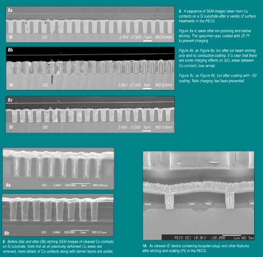
 Engineering Tripos Part IIB FOURTH YEAR Module 4B7: VLSI Design, Technology, and CAD Laboratory Experiment Dr D Holburn and Mr B Breton Scanning Electron Microscopical Examination of CMOS Integrated Circuit
7. Michelson Interferometer
 7. Michelson Interferometer In this lab we are going to observe the interference patterns produced by two spherical waves as well as by two plane waves. We will study the operation of a Michelson interferometer,
Lecture 20: Optical Tools for MEMS Imaging
 MECH 466 Microelectromechanical Systems University of Victoria Dept. of Mechanical Engineering Lecture 20: Optical Tools for MEMS Imaging 1 Overview Optical Microscopes Video Microscopes Scanning Electron
Today s Outline - January 25, C. Segre (IIT) PHYS Spring 2018 January 25, / 26
 PHYS Spring 2018 January 25, / 26") Today s Outline - January 25, 2018 C. Segre (IIT) PHYS 570 - Spring 2018 January 25, 2018 1 / 26 Today s Outline - January 25, 2018 HW #2 C. Segre (IIT) PHYS 570 - Spring 2018 January 25, 2018 1 / 26 Today
Today s Outline - January 25, 2018 C. Segre (IIT) PHYS 570 - Spring 2018 January 25, 2018 1 / 26 Today s Outline - January 25, 2018 HW #2 C. Segre (IIT) PHYS 570 - Spring 2018 January 25, 2018 1 / 26 Today
Full-screen mode Popup controls. Overview of the microscope user interface, TEM User Interface and TIA on the left and EDS on the right
 Quick Guide to Operating FEI Titan Themis G2 200 (S)TEM: TEM mode Susheng Tan Nanoscale Fabrication and Characterization Facility, University of Pittsburgh Office: M104/B01 Benedum Hall, 412-383-5978,
MSE 595T Transmission Electron Microscopy. Laboratory III TEM Imaging - I
 MSE 595T Basic Transmission Electron Microscopy TEM Imaging - I Purpose The purpose of this lab is to: 1. Make fine adjustments to the microscope alignment 2. Obtain a diffraction pattern 3. Obtain an
Recent results from the JEOL JEM-3000F FEGTEM in Oxford
 Recent results from the JEOL JEM-3000F FEGTEM in Oxford R.E. Dunin-Borkowski a, J. Sloan b, R.R. Meyer c, A.I. Kirkland c,d and J. L. Hutchison a a b c d Department of Materials, Parks Road, Oxford OX1
2. Raise HT to 200kVby following the procedure explained in 1.6.
 JEOL 2100 MANUAL Quick check list 1. If needed, fill the reservoir with LN2 2. Raise HT to 200kVby following the procedure explained in 1.6. 3. Insert specimen holder into TEM (Insert holder in airlock,
MICROSCOPE LAB. Resolving Power How well specimen detail is preserved during the magnifying process.
 AP BIOLOGY Cells ACTIVITY #2 MICROSCOPE LAB OBJECTIVES 1. Demonstrate proper care and use of a compound microscope. 2. Identify the parts of the microscope and describe the function of each part. 3. Compare
(1) Research Institute for Scientific Measurements, Tohoku University, Katahira 2-1-1, Aoba-ku,
 Research Institute for Scientific Measurements, Tohoku University, Katahira 2-1-1, Aoba-ku,") 351 Classification Physics Abstracts 07.80 Performance of a new high-resolution electron energy-loss spectroscopy microscope Masami Thrauchi(1), Ryuichi Kuzuo(1), Futami Satoh(1), Michiyoshi Thnaka(1),
351 Classification Physics Abstracts 07.80 Performance of a new high-resolution electron energy-loss spectroscopy microscope Masami Thrauchi(1), Ryuichi Kuzuo(1), Futami Satoh(1), Michiyoshi Thnaka(1),
A few concepts in TEM and STEM explained
 A few concepts in TEM and STEM explained Martin Ek November 23, 2011 1 Introduction This is a collection of short, qualitative explanations of key concepts in TEM and STEM. Most of them are beyond what
Instructions for Tecnai a brief start up manual
 Instructions for Tecnai a brief start up manual Version 3.0, 8.12.2015 Manual of Tecnai 12 transmission electron microscope located at Aalto University's Nanomicroscopy Center. More information of Nanomicroscopy
Scintillation Counters
 PHY311/312 Detectors for Nuclear and Particle Physics Dr. C.N. Booth Scintillation Counters Unlike many other particle detectors, which exploit the ionisation produced by the passage of a charged particle,
Algebra Based Physics. Reflection. Slide 1 / 66 Slide 2 / 66. Slide 3 / 66. Slide 4 / 66. Slide 5 / 66. Slide 6 / 66.
 Slide 1 / 66 Slide 2 / 66 lgebra ased Physics Geometric Optics 2015-12-01 www.njctl.org Slide 3 / 66 Slide 4 / 66 Table of ontents lick on the topic to go to that section Reflection Refraction and Snell's
INTRODUCTION THIN LENSES. Introduction. given by the paraxial refraction equation derived last lecture: Thin lenses (19.1) = 1. Double-lens systems
 = 1. Double-lens systems") Chapter 9 OPTICAL INSTRUMENTS Introduction Thin lenses Double-lens systems Aberrations Camera Human eye Compound microscope Summary INTRODUCTION Knowledge of geometrical optics, diffraction and interference,
Chapter 9 OPTICAL INSTRUMENTS Introduction Thin lenses Double-lens systems Aberrations Camera Human eye Compound microscope Summary INTRODUCTION Knowledge of geometrical optics, diffraction and interference,
Model SU3500 Scanning Electron Microscope
 Model SU3500 Scanning Electron Microscope Modified and Parts taken from Hitachi Easy Operation Guide. Before using the Model SU3500 SEM, be sure to read the [GENERAL SAFETY GUIDELINES] in the instruction
X-ray generation by femtosecond laser pulses and its application to soft X-ray imaging microscope
 X-ray generation by femtosecond laser pulses and its application to soft X-ray imaging microscope Kenichi Ikeda 1, Hideyuki Kotaki 1 ' 2 and Kazuhisa Nakajima 1 ' 2 ' 3 1 Graduate University for Advanced
Title: Amray 1830 SEM#2 Semiconductor & Microsystems Fabrication Laboratory Revision: D Rev Date: 03/18/2016
 Approved by: Process Engineer / / / / Equipment Engineer 1 SCOPE The purpose of this document is to detail the use of the Amray 1830 SEM. All users are expected to have read and understood this document.