Introduction to Electron Microscopy
|
|
|
- Damian Wilkins
- 5 years ago
- Views:
Transcription


1 Introduction to Electron Microscopy Prof. David Muller, Rm 274 Clark Hall, Ernst Ruska and Max Knoll built the first electron microscope in 1931 (Nobel Prize to Ruska in 1986) T4 Bacteriophage Electron Microscopy bridges the 1 nm 1 μm gap between x-ray diffraction and optical microscopy


")


2 Tools of the Trade AFM MFM Scanned Probe Microscope (includes Atomic Force Microscope) Transmission Electron Microscope Scanning Electron Microscope
3 Biological and Electronic Component Dimensions Biological Electronic Components Tool 1 Logic Board 10-2 Computer chip SEM Size (m) Mammalian cell Bacterial cell Optical Microscope TEM Virus Gene Protein Transistor Gate Oxide Atom AFM/STM
4 Comparison of Optical and Electron Microscopes Electron microscopes are operated in vacuum because the mean free path of electrons is air is short this mean biological samples should not degas they can either be dehydrated or frozen pathology, not in-vivo. Electron microscopes have higher resolution than optical microscopes atomic resolution is possible. Chemical imaging and spectroscopy mapping π and σ bonds at 1nm resolution can be done. Radiation damage is severe and limits the image quality and resolution (not as bad as x-rays or neutrons though! see R. Henderson, Quarterly Reviews of Biophysics 28 (1995) )
5 Comparison of Optical and Electron Microscopes Light Microscope source 1 st condenser TEM SEM or STEM 2 nd condenser Viewing screen Or CCD CA condenser aperture OA objective aperture SA selected area aperture specimen Objective lens Projector lenses Image formed by scanning a small spot Viewing screen Or CCD

6 Inside a Transmission Electron Microscope High tension cable ( kv) Filament condenser aperture Accelerating stack Double condenser lens objective aperture Sample sits here Selected area aperture Viewing chamber

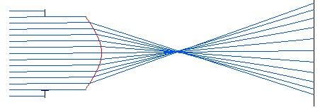
7 An Electron Lens
8 An Electron Lens
9 Geometric Optics A Simple Lens Focusing: angular deflection of ray α distance from optic axis θ x x Object plane front focal plane Lens at z=0 Back focal plane image plane
10 Geometric Optics A Simple Lens Wavefronts in focal plane are the Fourier Transform of the Image/Object θ 1 θ 1 x x Object plane front focal plane Lens at z=0 Back focal plane image plane

11 X-ray and Electron Diffraction from a Silicon Crystal Bragg s Law: n λ = d sinθ 10 kev x-rays 200 kev Electrons λ=1.54 Å λ=0.0251å In Si d 220 = 1.92 Å
12 Electron Velocity and Wavelength De Broglie Wavelength: λ = h p Where h is Planck s constant And p=mv are the momentum, mass and velocity of the electron If an electron is accelerated through a potential ev, it gains kinetic energy mv = ev So the momentum is mv = 2meV Electron wavelength λ = 2 h 1. 23nm = 2meV V (V in Volts) ( relativistically correct form: 2 h c ev (2m c λ ) = ev )
13 Electron Wavelength vs. Accelerating Voltage Relativistic Non-relativistic Accelerating Voltage v/c λ (Ǻ) λ (Angstroms) V 100 V 1 kev 10 kev 100 kev kev 300 kev MeV Electron Kinetic Energy (kev)
14 Resolution Limits Imposed by Spherical Aberration, C s (Or why we can t do subatomic imaging with a 100 kev electron) Lens C s >0 Plane of Least Confusion C s =0 d min Gaussian image plane For C s >0, rays far from the axis are bent too strongly and come to a crossover before the gaussian image plane. For a lens with aperture angle α, the minimum blur is d = min C s α Typical TEM numbers: C s = 1 mm, α=10 mrad d min = 0.5 nm
15 Resolution Limits Imposed by the Diffraction Limit (Less diffraction with a large aperture must be balanced against C s ) Lens α 0 d 0 d 0 Gaussian image plane The image of a point transferred through a lens with a circular aperture of semiangle α 0 is an Airy Disk of diameter 0.61λ = n sinα (for electrons, n~1, and the angles are small) λ α (0.61 for incoherent imaging e.g. ADF-STEM, 1.22 for coherent or phase contrast,. E.g TEM) 0
16 Balancing Spherical Aberration against the Diffraction Limit (Less diffraction with a large aperture must be balanced against C s ) For a rough estimate of the optimum aperture size, convolve blurring terms -If the point spreads were gaussian, we could add in quadrature: d 2 tot d d 2 s 0.61λ = α C α s Probe Size (Angstroms) 10 1 d s d α (mrad) d = Optimal aperture And minimum Spot size 1/ 4 3/ 4 min 0. 66C s λ
17 Balancing Spherical Aberration against the Diffraction Limit (Less diffraction with a large aperture must be balanced against C s ) A more accurate wave-optical treatment, allowing less than λ/4 of phase shift across the lens gives Minimum Spot size: d = 1/ 4 3/ 4 min 0. 43C s λ d = 1/ 4 3/ 4 min 0. 61C s λ (Incoherent image - e.g. STEM) (coherent image - e.g. TEM) Optimal aperture: α opt = 4λ Cs 1/ 4 At 200 kv, λ= Ǻ, d min = 1.53Ǻ and α opt = 10 mrad At 1 kv, λ=0.38 Ǻ, d min = 12 Ǻ and α opt = 20 mrad
![Electron Diffraction and Imaging a [100] Silicon Crystal](/docs-images/91/105312933/images/18-1.jpg "Image Diffraction Pattern 220 400 λ=0.0251å In Si d 220 = 1.")
18 Electron Diffraction and Imaging a [100] Silicon Crystal Image Diffraction Pattern λ=0.0251å In Si d 220 = 1.92 Å
19 Depth of Field, Depth of Focus D = 0 d tanα 0 For d=3nm, α=10 mrad, D 0 = 300 nm For d=200nm, α=0.1 mrad, D 0 = 2 mm!
20 Lenses in a Transmission Microscope (and deflection coils to correct their alignment) Gun: electron source If misaligned, low intensity & other alignments may also be out Condensor: uniformly illuminate the sample If misaligned, you will lose the beam when changing magnification Objective: image sample determines resolution. If misaligned, the image will be distorted, blurry. projector: magnifies image/ forms diffraction pattern should not alter resolution. If misaligned, the image will be distorted, diffraction pattern may be blurry.

21 Caustics in a Lens On-axis Tilted

22 Caustics (remove extreme rays and caustics by putting in an aperture) From Natural Focusing and Fine Structure of Light: Caustics and Wave Dislocations by J. F. Nye
23 Common Aberrations Astigmatism -x&y focus at different planes -fix by adjusting stigmators Bad Coma -beam is tilted off axis -fix by centering aperture Bad -Δf Δf=0 +Δf Good Good Check lens alignment by going through focus (change lens strength)
24 Lens Alignment Correcting for a gun shift misalignment How do we align one lens, when all lenses are misaligned? Step 1: Strongly excite C1 (small spot size) cross-over moves to lens & optic axis. Use beam shift D2 to bring spot to to axis below C2 Step 2: Weaken C1 (large spot size) cross-over moves away from optic axis Use gun shift D1 to bring spot to to axis below C2. Iterate until spot stops moving


25 Focusing using Fresnel Fringes 2 μm underfocus In focus 2 μm overfocus bright fringe Minimum contrast dark fringe Check lens alignment by going through focus (change lens strength)

26 Correcting Objective Astigmatism using Fresnel Fringes Astigmatic & best focus Stigmated& focused dark fringe bright fringe
27 Materials Microscopy Resources on Campus ( Type Atomic Force Microscopy Applications Topographic Imaging on wafers Accurate height measurements on flat surfaces (~ 0.5 nm vertical) Lateral Resolution nm In-situ no vacuum required Location Dr. Jonathan Shu D-22 Clark Hall Prof. Kit Umbach SB-60C Bard Hall CNF Clean Room Scanning Electron Microscopy Transmission Electron Microscopy Imaging of complex structures at 1-20 nm resolution X-ray mapping at nm In-vacuum Clark: High spatial resolution Snee/Bard: best x-ray mapping, OIM 1 nm (polymers) > atomic resolution of crystals in thin samples X-ray mapping at 1 nm EELS at < 1 nm Requires sample thinning (except for nanoparticles) Clark: Mick Thomas F3 Clark Hall Bard/Snee: John Hunt SB56 Bard/1149 Snee Duffield: John Grazul 150 Duffield (TEM+STEM) Clark: Mick Thomas F3 Clark (STEM+EDX)
Introduction to Electron Microscopy-II
 Introduction to Electron Microscopy-II Prof. David Muller, dm24@cornell.edu Rm 274 Clark Hall, 255-4065 Ernst Ruska and Max Knoll built the first electron microscope in 1931 (Nobel Prize to Ruska in 1986)
Transmission Electron Microscopy 9. The Instrument. Outline
 Transmission Electron Microscopy 9. The Instrument EMA 6518 Spring 2009 02/25/09 Outline The Illumination System The Objective Lens and Stage Forming Diffraction Patterns and Images Alignment and Stigmation
S200 Course LECTURE 1 TEM
 S200 Course LECTURE 1 TEM Development of Electron Microscopy 1897 Discovery of the electron (J.J. Thompson) 1924 Particle and wave theory (L. de Broglie) 1926 Electromagnetic Lens (H. Busch) 1932 Construction
Cs-corrector. Felix de Haas
 Cs-corrector. Felix de Haas Content Non corrector systems Lens aberrations and how to minimize? Corrector systems How is it done? Lens aberrations Spherical aberration Astigmatism Coma Chromatic Quality
Chapter 2 Instrumentation for Analytical Electron Microscopy Lecture 7. Chapter 2 CHEM Fall L. Ma
 Chapter 2 Instrumentation for Analytical Electron Microscopy Lecture 7 Outline Electron Sources (Electron Guns) Thermionic: LaB 6 or W Field emission gun: cold or Schottky Lenses Focusing Aberration Probe
Introduction to Transmission Electron Microscopy (Physical Sciences)
") Introduction to Transmission Electron Microscopy (Physical Sciences) Centre for Advanced Microscopy Program 9:30 10:45 Lecture 1 Basics of TEM 10:45 11:00 Morning tea 11:00 12:15 Lecture 2 Diffraction
Introduction to Transmission Electron Microscopy (Physical Sciences) Centre for Advanced Microscopy Program 9:30 10:45 Lecture 1 Basics of TEM 10:45 11:00 Morning tea 11:00 12:15 Lecture 2 Diffraction
The Resolution in the Electron Microscopy
 Volume 3, Issue, February 1 ISSN 319-87 The Resolution in the Electron Microscopy ABSTRACT Benefit from the group's equations, especially the resolution limits in the transmission electron microscope (TEM)
Electron
 Electron 1897: Sir Joseph John Thomson (1856-1940) discovered corpuscles small particles with a charge-to-mass ratio over 1000 times greater than that of protons. Plum pudding model : electrons in a sea
NANO 703-Notes. Chapter 9-The Instrument
 1 Chapter 9-The Instrument Illumination (condenser) system Before (above) the sample, the purpose of electron lenses is to form the beam/probe that will illuminate the sample. Our electron source is macroscopic
Introduction: Why electrons?
 Introduction: Why electrons? 1 Radiations Visible light X-rays Electrons Neutrons Advantages Not very damaging Easily focused Eye wonderful detector Small wavelength (Angstroms) Good penetration Small
Scanning Electron Microscopy. EMSE-515 F. Ernst
 Scanning Electron Microscopy EMSE-515 F. Ernst 1 2 Scanning Electron Microscopy Max Knoll Manfred von Ardenne Manfred von Ardenne Principle of Scanning Electron Microscopy 3 Principle of Scanning Electron
TEM theory Basic optics, image formation and key elements
 Workshop series of Chinese 3DEM community Get acquainted with Cryo-Electron Microscopy: First Chinese Workshop for Structural Biologists TEM theory Basic optics, image formation and key elements Jianlin
Low Voltage Electron Microscope
 LVEM5 Low Voltage Electron Microscope Nanoscale from your benchtop LVEM5 Delong America DELONG INSTRUMENTS COMPACT BUT POWERFUL The LVEM5 is designed to excel across a broad range of applications in material
A few concepts in TEM and STEM explained
 A few concepts in TEM and STEM explained Martin Ek November 23, 2011 1 Introduction This is a collection of short, qualitative explanations of key concepts in TEM and STEM. Most of them are beyond what
Scanning electron microscope
 Scanning electron microscope 6 th CEMM workshop Maja Koblar, Sc. Eng. Physics Outline The basic principle? What is an electron? Parts of the SEM Electron gun Electromagnetic lenses Apertures Chamber and
NanoSpective, Inc Progress Drive Suite 137 Orlando, Florida
 TEM Techniques Summary The TEM is an analytical instrument in which a thin membrane (typically < 100nm) is placed in the path of an energetic and highly coherent beam of electrons. Typical operating voltages
Nanotechnology and material science Lecture V
 Most widely used nanoscale microscopy. Based on possibility to create bright electron beam with sub-nm spot size. History: Ernst Ruska (1931), Nobel Prize (1986) For visible light λ=400-700nm, for electrons
GBS765 Hybrid methods
 GBS765 Hybrid methods Lecture 3 Contrast and image formation 10/20/14 4:37 PM The lens ray diagram Magnification M = A/a = v/u and 1/u + 1/v = 1/f where f is the focal length The lens ray diagram So we
CHAPTER TWO METALLOGRAPHY & MICROSCOPY
 CHAPTER TWO METALLOGRAPHY & MICROSCOPY 1. INTRODUCTION: Materials characterisation has two main aspects: Accurately measuring the physical, mechanical and chemical properties of materials Accurately measuring
ELECTRON MICROSCOPY. 13:10 16:00, Oct. 6, 2008 Institute of Physics, Academia Sinica. Tung Hsu
 ELECTRON MICROSCOPY 13:10 16:00, Oct. 6, 2008 Institute of Physics, Academia Sinica Tung Hsu Department of Materials Science and Engineering National Tsing Hua University Hsinchu 300, TAIWAN Tel. 03-5742564
Chapter 1. Basic Electron Optics (Lecture 2)
") Chapter 1. Basic Electron Optics (Lecture 2) Basic concepts of microscope (Cont ) Fundamental properties of electrons Electron Scattering Instrumentation Basic conceptions of microscope (Cont ) Ray diagram
Chapter 1. Basic Electron Optics (Lecture 2) Basic concepts of microscope (Cont ) Fundamental properties of electrons Electron Scattering Instrumentation Basic conceptions of microscope (Cont ) Ray diagram
PHY 431 Homework Set #5 Due Nov. 20 at the start of class
 PHY 431 Homework Set #5 Due Nov. 0 at the start of class 1) Newton s rings (10%) The radius of curvature of the convex surface of a plano-convex lens is 30 cm. The lens is placed with its convex side down
Chapter 4 Imaging Lecture 17
 Chapter 4 Imaging Lecture 17 d (110) Imaging Imaging in the TEM Diffraction Contrast in TEM Image HRTEM (High Resolution Transmission Electron Microscopy) Imaging STEM imaging Imaging in the TEM What is
Optical Components for Laser Applications. Günter Toesko - Laserseminar BLZ im Dezember
 Günter Toesko - Laserseminar BLZ im Dezember 2009 1 Aberrations An optical aberration is a distortion in the image formed by an optical system compared to the original. It can arise for a number of reasons
Lecture 20: Optical Tools for MEMS Imaging
 MECH 466 Microelectromechanical Systems University of Victoria Dept. of Mechanical Engineering Lecture 20: Optical Tools for MEMS Imaging 1 Overview Optical Microscopes Video Microscopes Scanning Electron
ELECTRON MICROSCOPY. 14:10 17:00, Apr. 3, 2007 Department of Physics, National Taiwan University. Tung Hsu
 ELECTRON MICROSCOPY 14:10 17:00, Apr. 3, 2007 Department of Physics, National Taiwan University Tung Hsu Department of Materials Science and Engineering National Tsinghua University Hsinchu 300, TAIWAN
A Tutorial on Electron Microscopy
 A Tutorial on Electron Microscopy Jian-Min (Jim) Zuo Mat. Sci. Eng. and Seitz-Materials Research Lab., UIUC Outline of This Tutorial I. Science and opportunities of electron microscopy II. The basic TEM,
Nanotechnology in Consumer Products
 Nanotechnology in Consumer Products Advances in Transmission Electron Microscopy Friday, April 21, 2017 October 31, 2014 The webinar will begin at 1pm Eastern Time Click here to watch the webinar recording
No part of this material may be reproduced without explicit written permission.
 This material is provided for educational use only. The information in these slides including all data, images and related materials are the property of : Robert M. Glaeser Department of Molecular & Cell
ELECTRON MICROSCOPY. 09:10 12:00, Oct. 27, 2006 Institute of Physics, Academia Sinica. Tung Hsu
 ELECTRON MICROSCOPY 09:10 12:00, Oct. 27, 2006 Institute of Physics, Academia Sinica Tung Hsu Department of Materials Science and Engineering National Tsinghua University Hsinchu 300, TAIWAN Tel. 03-5742564
STEM alignment procedures
 STEM alignment procedures Step 1. ASID alignment mode 1. Write down STD for TEM, and then open the ASID control window from dialogue. Also, start Simple imager viewer program on the Desktop. 2. Click on
Transmission electron Microscopy
 Transmission electron Microscopy Image formation of a concave lens in geometrical optics Some basic features of the transmission electron microscope (TEM) can be understood from by analogy with the operation
Low Voltage Electron Microscope. Nanoscale from your benchtop LVEM5. Delong America
 LVEM5 Low Voltage Electron Microscope Nanoscale from your benchtop LVEM5 Delong America DELONG INSTRUMENTS COMPACT BUT POWERFUL The LVEM5 is designed to excel across a broad range of applications in material
EE119 Introduction to Optical Engineering Spring 2003 Final Exam. Name:
 EE119 Introduction to Optical Engineering Spring 2003 Final Exam Name: SID: CLOSED BOOK. THREE 8 1/2 X 11 SHEETS OF NOTES, AND SCIENTIFIC POCKET CALCULATOR PERMITTED. TIME ALLOTTED: 180 MINUTES Fundamental
ELECTRON MICROSCOPY AN OVERVIEW
 ELECTRON MICROSCOPY AN OVERVIEW Anjali Priya 1, Abhishek Singh 2, Nikhil Anand Srivastava 3 1,2,3 Department of Electrical & Instrumentation, Sant Longowal Institute of Engg. & Technology, Sangrur, India.
MODULE I SCANNING ELECTRON MICROSCOPE (SEM)
") MODULE I SCANNING ELECTRON MICROSCOPE (SEM) Scanning Electron Microscope (SEM) Initially, the plan of SEM was offered by H. Stintzing in 1927 (a German patent application). His suggested procedure was
MODULE I SCANNING ELECTRON MICROSCOPE (SEM) Scanning Electron Microscope (SEM) Initially, the plan of SEM was offered by H. Stintzing in 1927 (a German patent application). His suggested procedure was
--> Buy True-PDF --> Auto-delivered in 0~10 minutes. JY/T
 Translated English of Chinese Standard: JY/T011-1996 www.chinesestandard.net Sales@ChineseStandard.net INDUSTRY STANDARD OF THE JY PEOPLE S REPUBLIC OF CHINA General rules for transmission electron microscopy
EE119 Introduction to Optical Engineering Fall 2009 Final Exam. Name:
 EE119 Introduction to Optical Engineering Fall 2009 Final Exam Name: SID: CLOSED BOOK. THREE 8 1/2 X 11 SHEETS OF NOTES, AND SCIENTIFIC POCKET CALCULATOR PERMITTED. TIME ALLOTTED: 180 MINUTES Fundamental
Physics 431 Final Exam Examples (3:00-5:00 pm 12/16/2009) TIME ALLOTTED: 120 MINUTES Name: Signature:
 TIME ALLOTTED: 120 MINUTES Name: Signature:") Physics 431 Final Exam Examples (3:00-5:00 pm 12/16/2009) TIME ALLOTTED: 120 MINUTES Name: PID: Signature: CLOSED BOOK. TWO 8 1/2 X 11 SHEET OF NOTES (double sided is allowed), AND SCIENTIFIC POCKET CALCULATOR
Physics 431 Final Exam Examples (3:00-5:00 pm 12/16/2009) TIME ALLOTTED: 120 MINUTES Name: PID: Signature: CLOSED BOOK. TWO 8 1/2 X 11 SHEET OF NOTES (double sided is allowed), AND SCIENTIFIC POCKET CALCULATOR
Tecnai on-line help manual --
 Tecnai on-line help Alignments 1 Tecnai on-line help manual -- Alignments Table of Contents 1 Alignments in the Tecnai microscope...5 2 Alignment procedures...6 3 Introduction to electron optics...11 3.1
MSE 460 TEM Lab 2: Basic Alignment and Operation of Microscope
 MSE 460 TEM Lab 2: Basic Alignment and Operation of Microscope Last updated on 1/8/2018 Jinsong Wu, jinsong-wu@northwestern.edu Aims: The aim of this lab is to familiarize you with basic TEM alignment
Phase plates for cryo-em
 Max Planck Institute of Biochemistry Martinsried, Germany MAX PLANCK SOCIETY Phase plates for cryo-em Rado Danev Max Planck Institute of Biochemistry, Martinsried, Germany. EMBO course 2017, London, UK
Introduction of New Products
 Field Emission Electron Microscope JEM-3100F For evaluation of materials in the fields of nanoscience and nanomaterials science, TEM is required to provide resolution and analytical capabilities that can
Point Spread Function. Confocal Laser Scanning Microscopy. Confocal Aperture. Optical aberrations. Alternative Scanning Microscopy
 Bi177 Lecture 5 Adding the Third Dimension Wide-field Imaging Point Spread Function Deconvolution Confocal Laser Scanning Microscopy Confocal Aperture Optical aberrations Alternative Scanning Microscopy
Electron Sources, Optics and Detectors
 Thomas LaGrange, Ph.D. Faculty Lecturer and Senior Staff Scientist Electron Sources, Optics and Detectors TEM Doctoral Course MS-637 April 16 th -18 th, 2018 Summary Electron propagation is only possible
VISUAL PHYSICS ONLINE DEPTH STUDY: ELECTRON MICROSCOPES
 VISUAL PHYSICS ONLINE DEPTH STUDY: ELECTRON MICROSCOPES Shortly after the experimental confirmation of the wave properties of the electron, it was suggested that the electron could be used to examine objects
SCANNING ELECTRON MICROSCOPY AND X-RAY MICROANALYSIS
 SCANNING ELECTRON MICROSCOPY AND X-RAY MICROANALYSIS Robert Edward Lee Electron Microscopy Center Department of Anatomy and Neurobiology Colorado State University P T R Prentice Hall, Englewood Cliffs,
Properties of optical instruments. Projection optical systems
 Properties of optical instruments Projection optical systems Instruments : optical systems designed for a specific function Projection systems: : real image (object real or at infinity) Examples: videoprojector,,
MSE 595T Transmission Electron Microscopy. Laboratory III TEM Imaging - I
 MSE 595T Basic Transmission Electron Microscopy TEM Imaging - I Purpose The purpose of this lab is to: 1. Make fine adjustments to the microscope alignment 2. Obtain a diffraction pattern 3. Obtain an
LECTURE 13 DIFFRACTION. Instructor: Kazumi Tolich
 LECTURE 13 DIFFRACTION Instructor: Kazumi Tolich Lecture 13 2 Reading chapter 33-4 & 33-6 to 33-7 Single slit diffraction Two slit interference-diffraction Fraunhofer and Fresnel diffraction Diffraction
Cardinal Points of an Optical System--and Other Basic Facts
 Cardinal Points of an Optical System--and Other Basic Facts The fundamental feature of any optical system is the aperture stop. Thus, the most fundamental optical system is the pinhole camera. The image
Scanning Transmission Electron Microscopy for Nanostructure Characterization
 6 Scanning Transmission Electron Microscopy for Nanostructure Characterization S. J. Pennycook, A. R. Lupini, M. Varela, A. Y. Borisevich, Y. Peng, M. P. Oxley, K. van Benthem, M. F. Chisholm 1. Introduction
Full-screen mode Popup controls. Overview of the microscope user interface, TEM User Interface and TIA on the left and EDS on the right
 Quick Guide to Operating FEI Titan Themis G2 200 (S)TEM: TEM mode Susheng Tan Nanoscale Fabrication and Characterization Facility, University of Pittsburgh Office: M104/B01 Benedum Hall, 412-383-5978,
Low Voltage Electron Microscope
 LVEM 25 Low Voltage Electron Microscope fast compact powerful Delong America FAST, COMPACT AND POWERFUL The LVEM 25 offers a high-contrast, high-throughput, and compact solution with nanometer resolutions.
Fabrication of Probes for High Resolution Optical Microscopy
 Fabrication of Probes for High Resolution Optical Microscopy Physics 564 Applied Optics Professor Andrès La Rosa David Logan May 27, 2010 Abstract Near Field Scanning Optical Microscopy (NSOM) is a technique
LVEM 25. Low Voltage Electron Mictoscope. fast compact powerful
 LVEM 25 Low Voltage Electron Mictoscope fast compact powerful FAST, COMPACT AND POWERFUL The LVEM 25 offers a high-contrast, high-throughput, and compact solution with nanometer resolutions. All the benefits
microscopy A great online resource Molecular Expressions, a Microscope Primer Partha Roy
 Fundamentals of optical microscopy A great online resource Molecular Expressions, a Microscope Primer http://micro.magnet.fsu.edu/primer/index.html Partha Roy 1 Why microscopy Topics Functions of a microscope
High Resolution Transmission Electron Microscopy (HRTEM) Summary 4/11/2018. Thomas LaGrange Faculty Lecturer and Senior Staff Scientist
 Summary 4/11/2018. Thomas LaGrange Faculty Lecturer and Senior Staff Scientist") Thomas LaGrange Faculty Lecturer and Senior Staff Scientist High Resolution Transmission Electron Microscopy (HRTEM) Doctoral Course MS-637 April 16-18th, 2018 Summary Contrast in TEM images results from
Thomas LaGrange Faculty Lecturer and Senior Staff Scientist High Resolution Transmission Electron Microscopy (HRTEM) Doctoral Course MS-637 April 16-18th, 2018 Summary Contrast in TEM images results from
BEAM HALO OBSERVATION BY CORONAGRAPH
 BEAM HALO OBSERVATION BY CORONAGRAPH T. Mitsuhashi, KEK, TSUKUBA, Japan Abstract We have developed a coronagraph for the observation of the beam halo surrounding a beam. An opaque disk is set in the beam
2.Components of an electron microscope. a) vacuum systems, b) electron guns, c) electron optics, d) detectors. Marco Cantoni, 021/
 vacuum systems, b) electron guns, c) electron optics, d) detectors. Marco Cantoni, 021/") 2.Components of an electron microscope a) vacuum systems, b) electron guns, c) electron optics, d) detectors Marco Cantoni, 021/693.48.16 Centre Interdisciplinaire de Microscopie Electronique CIME MSE-603
2.Components of an electron microscope a) vacuum systems, b) electron guns, c) electron optics, d) detectors Marco Cantoni, 021/693.48.16 Centre Interdisciplinaire de Microscopie Electronique CIME MSE-603
Atomic Resolution Imaging with a sub-50 pm Electron Probe
 Atomic Resolution Imaging with a sub-50 pm Electron Probe Rolf Erni, Marta D. Rossell, Christian Kisielowski, Ulrich Dahmen National Center for Electron Microscopy, Lawrence Berkeley National Laboratory
THE BOTTOM LINE I. THE MICROSCOPE
 THE BOTTOM LINE This document is designed to help students focus their attention on basic concepts that are important for understanding the fundamental principles of transmission electron microscopy, biological
Scanning Electron Microscopy Basics and Applications
 Scanning Electron Microscopy Basics and Applications Dr. Julia Deuschle Stuttgart Center for Electron Microscopy MPI for Solid State Research Room: 1E15, phone: 0711/ 689-1193 email: j.deuschle@fkf.mpg.de
Tutorial on Linear Image Simulations of Phase-Contrast and Incoherent Imaging by convolutions
 Tutorial on Linear Image Simulations of Phase-Contrast and Incoherent Imaging by convolutions Huolin Xin, David Muller, based on Appendix A of Kirkland s book This tutorial covers the use of temcon and
MSE 460 TEM Lab 4: Bright/Dark Field Imaging Operation
 MSE 460 TEM Lab 4: Bright/Dark Field Imaging Operation Last updated on 1/8/2018 Jinsong Wu, jinsong-wu@northwestern.edu Aims: The aim of this lab is to familiarize you with bright/dark field imaging operation.
Lecture 2: Geometrical Optics. Geometrical Approximation. Lenses. Mirrors. Optical Systems. Images and Pupils. Aberrations.
 Lecture 2: Geometrical Optics Outline 1 Geometrical Approximation 2 Lenses 3 Mirrors 4 Optical Systems 5 Images and Pupils 6 Aberrations Christoph U. Keller, Leiden Observatory, keller@strw.leidenuniv.nl
2.Components of an electron microscope. a) vacuum systems, b) electron guns, c) electron optics, d) detectors. Marco Cantoni 021/
 vacuum systems, b) electron guns, c) electron optics, d) detectors. Marco Cantoni 021/") 2.Components of an electron microscope a) vacuum systems, b) electron guns, c) electron optics, d) detectors, 021/693.48.16 Centre Interdisciplinaire de Microscopie Electronique CIME Summary Electron propagation
2.Components of an electron microscope a) vacuum systems, b) electron guns, c) electron optics, d) detectors, 021/693.48.16 Centre Interdisciplinaire de Microscopie Electronique CIME Summary Electron propagation
Katarina Logg, Kristofer Bodvard, Mikael Käll. Dept. of Applied Physics. 12 September Optical Microscopy. Supervisor s signature:...
 Katarina Logg, Kristofer Bodvard, Mikael Käll Dept. of Applied Physics 12 September 2007 O1 Optical Microscopy Name:.. Date:... Supervisor s signature:... Introduction Over the past decades, the number
Introduction to Scanning Electron Microscopy
 Introduction to Scanning Electron Microscopy By: Brandon Cheney Ant s Leg Integrated Circuit Nano-composite This document was created as part of a Senior Project in the Materials Engineering Department
Transmissions Electron Microscopy (TEM)
") Transmissions Electron Microscopy (TEM) Basic principles Diffraction Imaging Specimen preparation A.E. Gunnæs MENA3100 V17 TEM is based on three possible set of techniqes Diffraction From regions down
Transmissions Electron Microscopy (TEM) Basic principles Diffraction Imaging Specimen preparation A.E. Gunnæs MENA3100 V17 TEM is based on three possible set of techniqes Diffraction From regions down
Applied Optics. , Physics Department (Room #36-401) , ,
 , ,") Applied Optics Professor, Physics Department (Room #36-401) 2290-0923, 019-539-0923, shsong@hanyang.ac.kr Office Hours Mondays 15:00-16:30, Wednesdays 15:00-16:30 TA (Ph.D. student, Room #36-415) 2290-0921,
Applied Optics Professor, Physics Department (Room #36-401) 2290-0923, 019-539-0923, shsong@hanyang.ac.kr Office Hours Mondays 15:00-16:30, Wednesdays 15:00-16:30 TA (Ph.D. student, Room #36-415) 2290-0921,
Observing Microorganisms through a Microscope LIGHT MICROSCOPY: This type of microscope uses visible light to observe specimens. Compound Light Micros
 PHARMACEUTICAL MICROBIOLOGY JIGAR SHAH INSTITUTE OF PHARMACY NIRMA UNIVERSITY Observing Microorganisms through a Microscope LIGHT MICROSCOPY: This type of microscope uses visible light to observe specimens.
Chapter 3 Op,cal Instrumenta,on
 Imaging by an Op,cal System Change in curvature of wavefronts by a thin lens Chapter 3 Op,cal Instrumenta,on 3-1 Stops, Pupils, and Windows 3-4 The Camera 3-5 Simple Magnifiers and Eyepieces 1. Magnifiers
Heisenberg) relation applied to space and transverse wavevector
 relation applied to space and transverse wavevector") 2. Optical Microscopy 2.1 Principles A microscope is in principle nothing else than a simple lens system for magnifying small objects. The first lens, called the objective, has a short focal length (a
2. Optical Microscopy 2.1 Principles A microscope is in principle nothing else than a simple lens system for magnifying small objects. The first lens, called the objective, has a short focal length (a
EE-527: MicroFabrication
 EE-57: MicroFabrication Exposure and Imaging Photons white light Hg arc lamp filtered Hg arc lamp excimer laser x-rays from synchrotron Electrons Ions Exposure Sources focused electron beam direct write
Low-energy Electron Diffractive Imaging for Three dimensional Light-element Materials
 Low-energy Electron Diffractive Imaging for Three dimensional Light-element Materials Hitachi Review Vol. 61 (2012), No. 6 269 Osamu Kamimura, Ph. D. Takashi Dobashi OVERVIEW: Hitachi has been developing
Titan on-line help manual -- Working with a FEG
 1 manual -- Working with a FEG Table of Contents 1 FEG Safety... 2 1.1 The column valves... 2 2 FEG States... 2 3 Starting the FEG... 4 4 Shutting the FEG down... 6 5 FEG Design... 6 5.1 Electron source...
(Refer Slide Time: 00:10)
") Fundamentals of optical and scanning electron microscopy Dr. S. Sankaran Department of Metallurgical and Materials Engineering Indian Institute of Technology, Madras Module 03 Unit-6 Instrumental details
Fundamentals of optical and scanning electron microscopy Dr. S. Sankaran Department of Metallurgical and Materials Engineering Indian Institute of Technology, Madras Module 03 Unit-6 Instrumental details
Lecture 2: Geometrical Optics. Geometrical Approximation. Lenses. Mirrors. Optical Systems. Images and Pupils. Aberrations.
 Lecture 2: Geometrical Optics Outline 1 Geometrical Approximation 2 Lenses 3 Mirrors 4 Optical Systems 5 Images and Pupils 6 Aberrations Christoph U. Keller, Leiden Observatory, keller@strw.leidenuniv.nl
Manufacturing Metrology Team
 The Team has a range of state-of-the-art equipment for the measurement of surface texture and form. We are happy to discuss potential measurement issues and collaborative research Manufacturing Metrology
Topics 3b,c Electron Microscopy
 Topics 3b,c Electron Microscopy 1.0 Introduction and History 1.1 Characteristic Information 2.0 Basic Principles 2.1 Electron-Solid Interactions 2.2 Electromagnetic Lenses 2.3 Breakdown of an Electron
Modulation Transfer Function
 Modulation Transfer Function The Modulation Transfer Function (MTF) is a useful tool in system evaluation. t describes if, and how well, different spatial frequencies are transferred from object to image.
ECEG105/ECEU646 Optics for Engineers Course Notes Part 4: Apertures, Aberrations Prof. Charles A. DiMarzio Northeastern University Fall 2008
 ECEG105/ECEU646 Optics for Engineers Course Notes Part 4: Apertures, Aberrations Prof. Charles A. DiMarzio Northeastern University Fall 2008 July 2003+ Chuck DiMarzio, Northeastern University 11270-04-1
Scanning electron microscope
 Scanning electron microscope 5 th CEMM workshop Maja Koblar, Sc. Eng. Physics Outline The basic principle? What is an electron? Parts of the SEM Electron gun Electromagnetic lenses Apertures Detectors
Why is There a Black Dot when Defocus = 1λ?
 Why is There a Black Dot when Defocus = 1λ? W = W 020 = a 020 ρ 2 When a 020 = 1λ Sag of the wavefront at full aperture (ρ = 1) = 1λ Sag of the wavefront at ρ = 0.707 = 0.5λ Area of the pupil from ρ =
Module 4B7: VLSI Design, Technology, and CAD. Scanning Electron Microscopical Examination of CMOS Integrated Circuit
 Engineering Tripos Part IIB FOURTH YEAR Module 4B7: VLSI Design, Technology, and CAD Laboratory Experiment Dr D Holburn and Mr B Breton Scanning Electron Microscopical Examination of CMOS Integrated Circuit
Chapter 34 The Wave Nature of Light; Interference. Copyright 2009 Pearson Education, Inc.
 Chapter 34 The Wave Nature of Light; Interference 34-7 Luminous Intensity The intensity of light as perceived depends not only on the actual intensity but also on the sensitivity of the eye at different
1.2. Make sure the viewing screen is covered (exposure to liquid N 2 may cause it to crack).
.") FEI Tecnai F20 S/TEM: imaging in TEM mode Nicholas G. Rudawski ngr@ufl.edu (805) 252-4916 (352) 392-3077 Last updated: 01/21/18 1. Filling the cold trap (if needed) 1.1. Prior to use, the cold trap needs
FEI Tecnai F20 S/TEM: imaging in TEM mode Nicholas G. Rudawski ngr@ufl.edu (805) 252-4916 (352) 392-3077 Last updated: 01/21/18 1. Filling the cold trap (if needed) 1.1. Prior to use, the cold trap needs
p q p f f f q f p q f NANO 703-Notes Chapter 5-Magnification and Electron Sources
 Chapter 5-agnification and Electron Sources Lens equation Let s first consider the properties of an ideal lens. We want rays diverging from a point on an object in front of the lens to converge to a corresponding
Properties of optical instruments. Visual optical systems part 2: focal visual instruments (microscope type)
") Properties of optical instruments Visual optical systems part 2: focal visual instruments (microscope type) Examples of focal visual instruments magnifying glass Eyepieces Measuring microscopes from the
Properties of optical instruments Visual optical systems part 2: focal visual instruments (microscope type) Examples of focal visual instruments magnifying glass Eyepieces Measuring microscopes from the
Development of JEM-2800 High Throughput Electron Microscope
 Development of JEM-2800 High Throughput Electron Microscope Mitsuhide Matsushita, Shuji Kawai, Takeshi Iwama, Katsuhiro Tanaka, Toshiko Kuba and Noriaki Endo EM Business Unit, JEOL Ltd. Electron Optics
Microscope anatomy, image formation and resolution
 Microscope anatomy, image formation and resolution Ian Dobbie Buy this book for your lab: D.B. Murphy, "Fundamentals of light microscopy and electronic imaging", ISBN 0-471-25391-X Visit these websites:
Microscopy: Fundamental Principles and Practical Approaches
 Microscopy: Fundamental Principles and Practical Approaches Simon Atkinson Online Resource: http://micro.magnet.fsu.edu/primer/index.html Book: Murphy, D.B. Fundamentals of Light Microscopy and Electronic
Aberrations and adaptive optics for biomedical microscopes
 Aberrations and adaptive optics for biomedical microscopes Martin Booth Department of Engineering Science And Centre for Neural Circuits and Behaviour University of Oxford Outline Rays, wave fronts and
Microscopy. ( greek mikros = small; skopein = to observe)
") Microscopy ( greek mikros = small; skopein = to observe) Zacharias Jansen put several lenses in a tube (first compound microscope) and the object near the end of tube appeared to be greatly enlarged, much
Microscopy ( greek mikros = small; skopein = to observe) Zacharias Jansen put several lenses in a tube (first compound microscope) and the object near the end of tube appeared to be greatly enlarged, much
Lab 05: Transmission Electron Microscopy
 Lab 05: Transmission Electron Microscopy Author: Mike Nill Alex Bryant Contents 1 Introduction 2 1.1 Imaging Modes....................................... 2 1.2 Electromagnetic Lenses..................................
JEM-F200. Multi-purpose Electron Microscope. Scientific / Metrology Instruments Multi-purpose Electron Microscope
 Scientific / Metrology Instruments Multi-purpose Electron Microscope JEM-F200 Multi-purpose Electron Microscope JEM-F200/F2 is a multi-purpose electron microscope of the new generation to meet today's
Microscope. Dr. Leena Barhate Department of Microbiology M.J.College, Jalgaon
 Microscope Dr. Leena Barhate Department of Microbiology M.J.College, Jalgaon Acknowledgement http://www.cerebromente.org.br/n17/histor y/neurons1_i.htm Google Images http://science.howstuffworks.com/lightmicroscope1.htm
(1) Research Institute for Scientific Measurements, Tohoku University, Katahira 2-1-1, Aoba-ku,
 Research Institute for Scientific Measurements, Tohoku University, Katahira 2-1-1, Aoba-ku,") 351 Classification Physics Abstracts 07.80 Performance of a new high-resolution electron energy-loss spectroscopy microscope Masami Thrauchi(1), Ryuichi Kuzuo(1), Futami Satoh(1), Michiyoshi Thnaka(1),
351 Classification Physics Abstracts 07.80 Performance of a new high-resolution electron energy-loss spectroscopy microscope Masami Thrauchi(1), Ryuichi Kuzuo(1), Futami Satoh(1), Michiyoshi Thnaka(1),