Scanning Electron Microscopy. EMSE-515 F. Ernst
|
|
|
- Marylou Hubbard
- 5 years ago
- Views:
Transcription
1 Scanning Electron Microscopy EMSE-515 F. Ernst 1


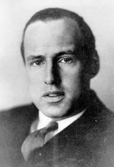
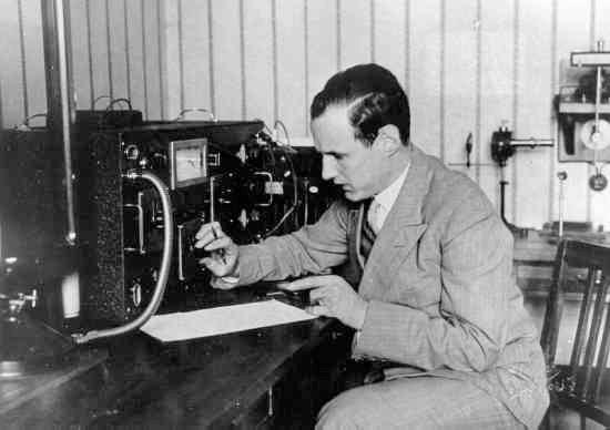
2 2 Scanning Electron Microscopy Max Knoll Manfred von Ardenne Manfred von Ardenne


3 Principle of Scanning Electron Microscopy 3

4 Principle of Scanning Electron Microscopy 4
5 Animated Demonstration of SEM 5

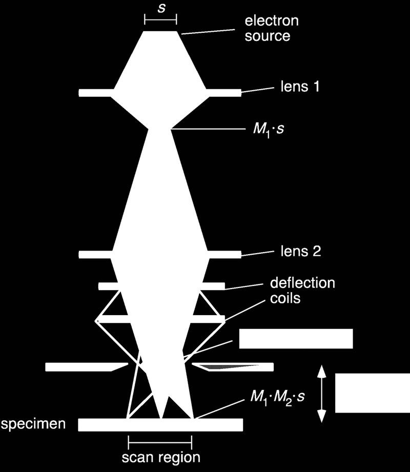
6 Principle of Scanning Electron Microscopy focused electron beam specimen: emits electrons and photons detector: electrons, photons, amplifier brightness of corresponding pixel deflection coils: scan the beam image scanning electronmicroscopy SEM no imaging electron optics! 6
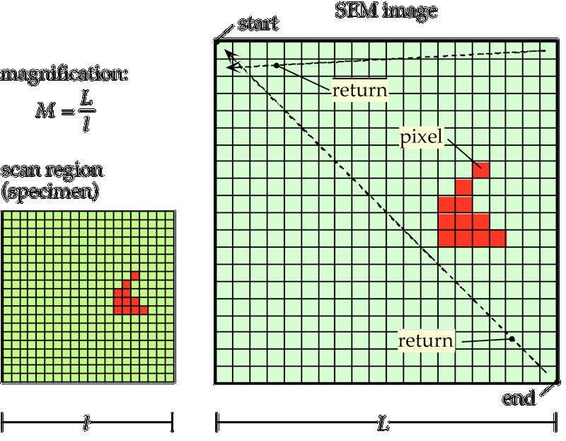
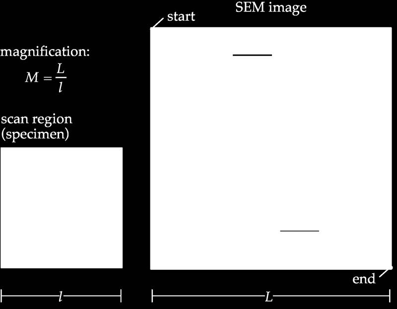
7 Magnification 7
, backscattered electrons (B) photons: X-rays, light, heat, complementary information from the same region of the specimen")
8 Advantages of SEM easy to change magnification can use manifold of emissions from the specimen, e. g.: electrons: secondary electrons (S), backscattered electrons (B) photons: X-rays, light, heat, complementary information from the same region of the specimen electronic processing: contrast amplification noise reduction 8
9 Realization

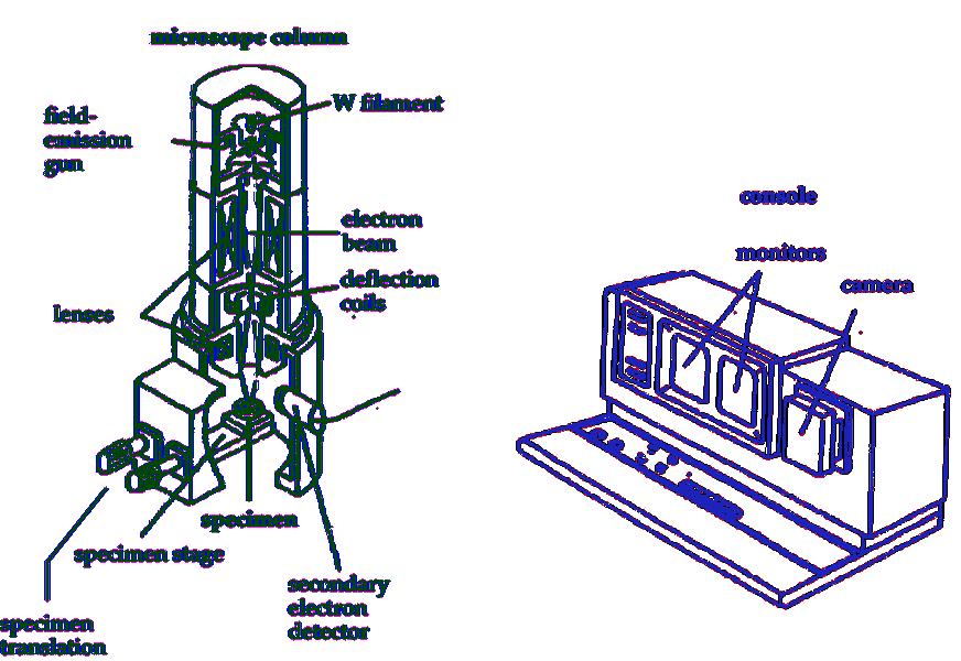
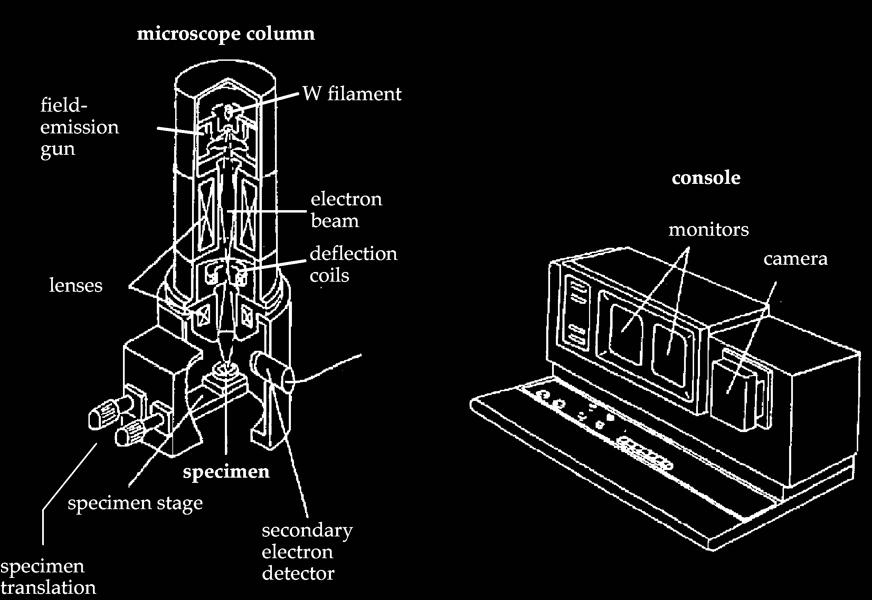
10 Field-Emission Gun Scanning Electron Microscope Hitachi S
 system spatial resolution: < 1.5 nm at 15 kev electron energy also performs well at reduced beam energies (e. g.")
11 Field-Emission Gun Scanning Electron Microscope Hitachi S4500 field-emission gun two secondary electron detectors backscatter detector infrared chamber scope Noran XEDS (X-ray energy-dispersive spectrometry) system spatial resolution: < 1.5 nm at 15 kev electron energy also performs well at reduced beam energies (e. g. 1 kev) facilitates observation of insulating materials emphasizes near-surface structure of the specimen 11

12 Environmental Scanning Electron Microscope Philips XL30 12
 heating stage, up to 1500 C OIM (orientation imaging microscopy) EBSP (electron backscatter pattern) detector automated determination of crystal")
13 Environmental Scanning Electron Microscope Philips XL30 usual SEM capabilities for imaging and microanalysis, plus: imaging in various gases including water vapor pressures up to 20 mbar cooling stage tensile stage (capable of heating up to 1000 C) heating stage, up to 1500 C OIM (orientation imaging microscopy) EBSP (electron backscatter pattern) detector automated determination of crystal orientation 13

14 ESEM Applications pharmaceutical dynamic physio-chemical properties e. g. swelling, disintegration and dissolution of drugs fiber technology: wetting and drying of wool, cotton and synthetic fibers cement science observe how water reacts with cements e ects of additives on the cementing process medical: observe fresh and wet tissue biology/botany/entomology: live (!) plant seedlings, ants, fleas 14
 requires UHV (< 10 7 Pa), to keep tip clean anode ground potential potential di erence versus cathode: 0.5.")
15 Electron Beam Formation electron gun: thermal emission tungsten filament or LaB 6 single crystal requires vacuum < 10 5 Pa field-emission (tunneling e ect): pointed tungsten tip ( strong electric field) requires UHV (< 10 7 Pa), to keep tip clean anode ground potential potential di erence versus cathode: kv


16 Electron Beam Formation 16

17 Tungsten Filament 17

18 LaB 6 Filament 18
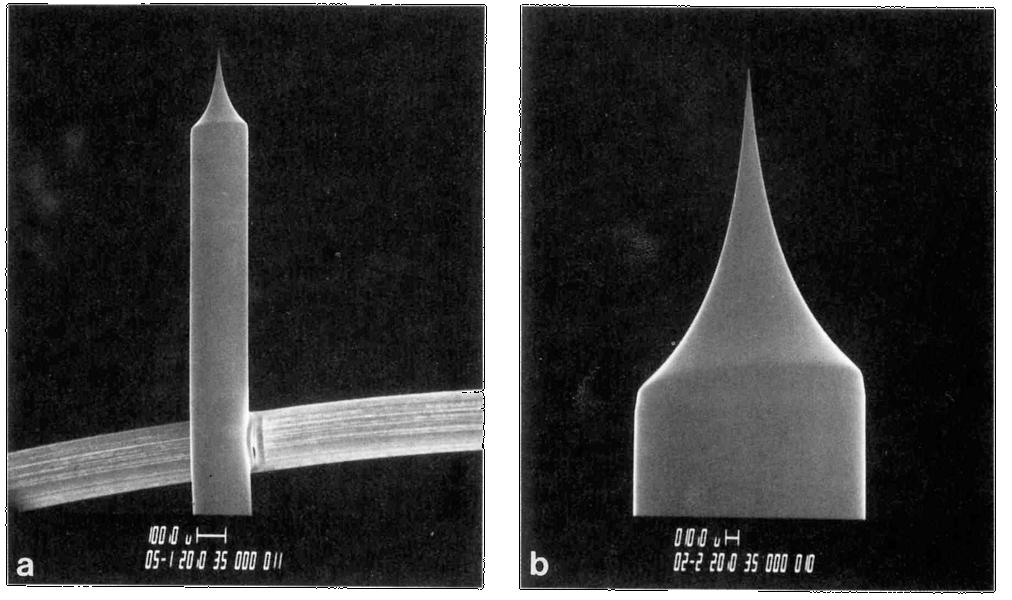
19 Field-Emission Tip 19

20 Instrument Capabilities and Limitations brightness of the electron gun definition: current density (A/m 2 ) per solid angle (sr) (steradian) LaB 6 cathode: 10 times brighter than tungsten cathode field-emission gun: 100 times brighter than LaB 6 typical brightness of a field-emission gun: > A m 2 sr 1 20
21 Instrument Capabilities and Limitations minimum beam diameter d small beam diameter requires reduction of source image by condensor system typical condensor system: two electromagnetic lenses minimum beam diameter in practice: µm for thermal emission (LaB 6 ) 10 nm for field-emission gun 21

22 Ray Path 22

23 Instrument Capabilities and Limitations beam convergence (semi-angle of the beam cone) aperture in the plane where beam position independent of the scan point (tilt angle) aperture diameter determines beam convergence resolution limit : > d high resolution requires small beam diameter but: current I 0 into the specimen decreases rapidly with decreasing beam diameter d: I 0 2 d 2 : semi-angle of the beam cone ( convergence angle). 23

24 Instrument Capabilities and Limitations aberrations of the illumination system increase the theoretical beam diameter d to d = d2 + 2 C s d 0 : true beam diameter; C s : coe cient of spherical aberration; : de Broglie wavelength of the electrons. both, very large and very small beam convergence are disadvantageous 24
25 Instrument Capabilities and Limitations general problem: SEM does not make optimum use of illumination to optimize SEM performance: choose beam convergence for maximum beam current I 0 (for given beam diameter d, determined by required resolution) depth of focus: D f := pixel diameter in specimen plane typical value: pixel diameter 100 very large! 25
: contrast C must exceed noise by factor 5 detail with contrast C visible only if I B > Q")
26 Signal-to-Noise Ratio definition of contrast C of image detail: C := S S S: average signal level; S: increase at region of interest. noise: random fluctuations of signal level around S visibility of a detail (empirical criterion): contrast C must exceed noise by factor 5 detail with contrast C visible only if I B > Q 0 C 2 : readout time per image; Q 0 = As. 26

27 Signal-to-Noise Ratio definition of contrast C of image detail: observation of details with weak contrast: long exposure time, or large beam current fundamental limit of resolution imposed by: gun brightness aberrations 27
SCANNING ELECTRON MICROSCOPY AND X-RAY MICROANALYSIS
 SCANNING ELECTRON MICROSCOPY AND X-RAY MICROANALYSIS Robert Edward Lee Electron Microscopy Center Department of Anatomy and Neurobiology Colorado State University P T R Prentice Hall, Englewood Cliffs,
S200 Course LECTURE 1 TEM
 S200 Course LECTURE 1 TEM Development of Electron Microscopy 1897 Discovery of the electron (J.J. Thompson) 1924 Particle and wave theory (L. de Broglie) 1926 Electromagnetic Lens (H. Busch) 1932 Construction
MODULE I SCANNING ELECTRON MICROSCOPE (SEM)
") MODULE I SCANNING ELECTRON MICROSCOPE (SEM) Scanning Electron Microscope (SEM) Initially, the plan of SEM was offered by H. Stintzing in 1927 (a German patent application). His suggested procedure was
MODULE I SCANNING ELECTRON MICROSCOPE (SEM) Scanning Electron Microscope (SEM) Initially, the plan of SEM was offered by H. Stintzing in 1927 (a German patent application). His suggested procedure was
Functions of the SEM subsystems
 Functions of the SEM subsystems Electronic column It consists of an electron gun and two or more electron lenses, which influence the path of electrons traveling down an evacuated tube. The base of the
Scanning Electron Microscopy SEM. Warren Straszheim, PhD MARL, 23 Town Engineering
 Scanning Electron Microscopy SEM Warren Straszheim, PhD MARL, 23 Town Engineering wesaia@iastate.edu 515-294-8187 How it works Create a focused electron beam Accelerate it Scan it across the sample Map
2.Components of an electron microscope. a) vacuum systems, b) electron guns, c) electron optics, d) detectors. Marco Cantoni 021/
 vacuum systems, b) electron guns, c) electron optics, d) detectors. Marco Cantoni 021/") 2.Components of an electron microscope a) vacuum systems, b) electron guns, c) electron optics, d) detectors, 021/693.48.16 Centre Interdisciplinaire de Microscopie Electronique CIME Summary Electron propagation
2.Components of an electron microscope a) vacuum systems, b) electron guns, c) electron optics, d) detectors, 021/693.48.16 Centre Interdisciplinaire de Microscopie Electronique CIME Summary Electron propagation
Scanning electron microscope
 Scanning electron microscope 6 th CEMM workshop Maja Koblar, Sc. Eng. Physics Outline The basic principle? What is an electron? Parts of the SEM Electron gun Electromagnetic lenses Apertures Chamber and
Electron Sources, Optics and Detectors
 Thomas LaGrange, Ph.D. Faculty Lecturer and Senior Staff Scientist Electron Sources, Optics and Detectors TEM Doctoral Course MS-637 April 16 th -18 th, 2018 Summary Electron propagation is only possible
Scanning electron microscope
 Scanning electron microscope 5 th CEMM workshop Maja Koblar, Sc. Eng. Physics Outline The basic principle? What is an electron? Parts of the SEM Electron gun Electromagnetic lenses Apertures Detectors
2.Components of an electron microscope. a) vacuum systems, b) electron guns, c) electron optics, d) detectors. Marco Cantoni, 021/
 vacuum systems, b) electron guns, c) electron optics, d) detectors. Marco Cantoni, 021/") 2.Components of an electron microscope a) vacuum systems, b) electron guns, c) electron optics, d) detectors Marco Cantoni, 021/693.48.16 Centre Interdisciplinaire de Microscopie Electronique CIME MSE-603
2.Components of an electron microscope a) vacuum systems, b) electron guns, c) electron optics, d) detectors Marco Cantoni, 021/693.48.16 Centre Interdisciplinaire de Microscopie Electronique CIME MSE-603
Introduction to Electron Microscopy
 Introduction to Electron Microscopy Prof. David Muller, dm24@cornell.edu Rm 274 Clark Hall, 255-4065 Ernst Ruska and Max Knoll built the first electron microscope in 1931 (Nobel Prize to Ruska in 1986)
Introduction to Scanning Electron Microscopy
 Introduction to Scanning Electron Microscopy By: Brandon Cheney Ant s Leg Integrated Circuit Nano-composite This document was created as part of a Senior Project in the Materials Engineering Department
Scanning Electron Microscopy Basics and Applications
 Scanning Electron Microscopy Basics and Applications Dr. Julia Deuschle Stuttgart Center for Electron Microscopy MPI for Solid State Research Room: 1E15, phone: 0711/ 689-1193 email: j.deuschle@fkf.mpg.de
p q p f f f q f p q f NANO 703-Notes Chapter 5-Magnification and Electron Sources
 Chapter 5-agnification and Electron Sources Lens equation Let s first consider the properties of an ideal lens. We want rays diverging from a point on an object in front of the lens to converge to a corresponding
Transmission Electron Microscopy 9. The Instrument. Outline
 Transmission Electron Microscopy 9. The Instrument EMA 6518 Spring 2009 02/25/09 Outline The Illumination System The Objective Lens and Stage Forming Diffraction Patterns and Images Alignment and Stigmation
Introduction: Why electrons?
 Introduction: Why electrons? 1 Radiations Visible light X-rays Electrons Neutrons Advantages Not very damaging Easily focused Eye wonderful detector Small wavelength (Angstroms) Good penetration Small
Topics 3b,c Electron Microscopy
 Topics 3b,c Electron Microscopy 1.0 Introduction and History 1.1 Characteristic Information 2.0 Basic Principles 2.1 Electron-Solid Interactions 2.2 Electromagnetic Lenses 2.3 Breakdown of an Electron
SCIENTIFIC INSTRUMENT NEWS. Introduction. Design of the FlexSEM 1000
 SCIENTIFIC INSTRUMENT NEWS 2017 Vol. 9 SEPTEMBER Technical magazine of Electron Microscope and Analytical Instruments. Technical Explanation The FlexSEM 1000: A Scanning Electron Microscope Specializing
Nanotechnology and material science Lecture V
 Most widely used nanoscale microscopy. Based on possibility to create bright electron beam with sub-nm spot size. History: Ernst Ruska (1931), Nobel Prize (1986) For visible light λ=400-700nm, for electrons
Chapter 1. Basic Electron Optics (Lecture 2)
") Chapter 1. Basic Electron Optics (Lecture 2) Basic concepts of microscope (Cont ) Fundamental properties of electrons Electron Scattering Instrumentation Basic conceptions of microscope (Cont ) Ray diagram
Chapter 1. Basic Electron Optics (Lecture 2) Basic concepts of microscope (Cont ) Fundamental properties of electrons Electron Scattering Instrumentation Basic conceptions of microscope (Cont ) Ray diagram
ELECTRON MICROSCOPY. 13:10 16:00, Oct. 6, 2008 Institute of Physics, Academia Sinica. Tung Hsu
 ELECTRON MICROSCOPY 13:10 16:00, Oct. 6, 2008 Institute of Physics, Academia Sinica Tung Hsu Department of Materials Science and Engineering National Tsing Hua University Hsinchu 300, TAIWAN Tel. 03-5742564
Introduction to Electron Microscopy-II
 Introduction to Electron Microscopy-II Prof. David Muller, dm24@cornell.edu Rm 274 Clark Hall, 255-4065 Ernst Ruska and Max Knoll built the first electron microscope in 1931 (Nobel Prize to Ruska in 1986)
Low Voltage Electron Microscope
 LVEM5 Low Voltage Electron Microscope Nanoscale from your benchtop LVEM5 Delong America DELONG INSTRUMENTS COMPACT BUT POWERFUL The LVEM5 is designed to excel across a broad range of applications in material
Introduction of New Products
 Field Emission Electron Microscope JEM-3100F For evaluation of materials in the fields of nanoscience and nanomaterials science, TEM is required to provide resolution and analytical capabilities that can
Lecture 20: Optical Tools for MEMS Imaging
 MECH 466 Microelectromechanical Systems University of Victoria Dept. of Mechanical Engineering Lecture 20: Optical Tools for MEMS Imaging 1 Overview Optical Microscopes Video Microscopes Scanning Electron
ELECTRON MICROSCOPY. 14:10 17:00, Apr. 3, 2007 Department of Physics, National Taiwan University. Tung Hsu
 ELECTRON MICROSCOPY 14:10 17:00, Apr. 3, 2007 Department of Physics, National Taiwan University Tung Hsu Department of Materials Science and Engineering National Tsinghua University Hsinchu 300, TAIWAN
Examination, TEN1, in courses SK2500/SK2501, Physics of Biomedical Microscopy,
 KTH Applied Physics Examination, TEN1, in courses SK2500/SK2501, Physics of Biomedical Microscopy, 2009-06-05, 8-13, FB51 Allowed aids: Compendium Imaging Physics (handed out) Compendium Light Microscopy
ELECTRON MICROSCOPY AN OVERVIEW
 ELECTRON MICROSCOPY AN OVERVIEW Anjali Priya 1, Abhishek Singh 2, Nikhil Anand Srivastava 3 1,2,3 Department of Electrical & Instrumentation, Sant Longowal Institute of Engg. & Technology, Sangrur, India.
How to choose a Scanning Electron Microscope (SEM)
") www.lambdaphoto.co.uk E-guide How to choose a Scanning Electron Microscope (SEM) Providing guidance in the selection of the right microscope for your research Distribution in the UK & Ireland Table of
www.lambdaphoto.co.uk E-guide How to choose a Scanning Electron Microscope (SEM) Providing guidance in the selection of the right microscope for your research Distribution in the UK & Ireland Table of
Oct. 30th- Nov. 1st, 2017
 Thomas LaGrange, Ph.D. Faculty Lecturer and Senior Staff Scientist Electron Sources, Optics and Detectors SEM Doctoral Course MS-636 Oct. 30th- Nov. 1st, 2017 Summary Electron propagation is only possible
Scanning Electron Microscopy
 Scanning Electron Microscopy For the semiconductor industry A tutorial Titel Vorname Nachname Titel Jobtitle, Bereich/Abteilung Overview Scanning Electron microscopy Scanning Electron Microscopy (SEM)
Oct. 30th- Nov. 1st, 2017
 Thomas LaGrange, Ph.D. Faculty Lecturer and Senior Staff Scientist Electron Sources, Optics and Detectors SEM Doctoral Course MS-636 Oct. 30th- Nov. 1st, 2017 Summary Electron propagation is only possible
VISUAL PHYSICS ONLINE DEPTH STUDY: ELECTRON MICROSCOPES
 VISUAL PHYSICS ONLINE DEPTH STUDY: ELECTRON MICROSCOPES Shortly after the experimental confirmation of the wave properties of the electron, it was suggested that the electron could be used to examine objects
Low Voltage Electron Microscope. Nanoscale from your benchtop LVEM5. Delong America
 LVEM5 Low Voltage Electron Microscope Nanoscale from your benchtop LVEM5 Delong America DELONG INSTRUMENTS COMPACT BUT POWERFUL The LVEM5 is designed to excel across a broad range of applications in material
The light microscope
 What is a microscope? The microscope is an essential tool in modern biology. It allows us to view structural details of organs, tissue, and cells not visible to the naked eye. The microscope should always
SECONDARY ELECTRON DETECTION
 SECONDARY ELECTRON DETECTION CAMTEC Workshop Presentation Haitian Xu June 14 th 2010 Introduction SEM Raster scan specimen surface with focused high energy e- beam Signal produced by beam interaction with
Very short introduction to light microscopy and digital imaging
 Very short introduction to light microscopy and digital imaging Hernan G. Garcia August 1, 2005 1 Light Microscopy Basics In this section we will briefly describe the basic principles of operation and
Design and fabrication of a scanning electron microscope using a finite element analysis for electron optical system
 Journal of Mechanical Science and Technology 22 (2008) 1734~1746 Journal of Mechanical Science and Technology www.springerlink.com/content/1738-494x DOI 10.1007/s12206-008-0317-9 Design and fabrication
Observing Microorganisms through a Microscope LIGHT MICROSCOPY: This type of microscope uses visible light to observe specimens. Compound Light Micros
 PHARMACEUTICAL MICROBIOLOGY JIGAR SHAH INSTITUTE OF PHARMACY NIRMA UNIVERSITY Observing Microorganisms through a Microscope LIGHT MICROSCOPY: This type of microscope uses visible light to observe specimens.
Transmission electron Microscopy
 Transmission electron Microscopy Image formation of a concave lens in geometrical optics Some basic features of the transmission electron microscope (TEM) can be understood from by analogy with the operation
Low Voltage Electron Microscope
 LVEM 25 Low Voltage Electron Microscope fast compact powerful Delong America FAST, COMPACT AND POWERFUL The LVEM 25 offers a high-contrast, high-throughput, and compact solution with nanometer resolutions.
Schottky Emission VP FE-SEM
 Schottky Emission VP FE-SEM Variable Pressure The Scanning Electron Microscope (SEM) has played an important role for many years for research and development of advanced materials in the leading edge of
Microscopy. ( greek mikros = small; skopein = to observe)
") Microscopy ( greek mikros = small; skopein = to observe) Zacharias Jansen put several lenses in a tube (first compound microscope) and the object near the end of tube appeared to be greatly enlarged, much
Microscopy ( greek mikros = small; skopein = to observe) Zacharias Jansen put several lenses in a tube (first compound microscope) and the object near the end of tube appeared to be greatly enlarged, much
LVEM 25. Low Voltage Electron Mictoscope. fast compact powerful
 LVEM 25 Low Voltage Electron Mictoscope fast compact powerful FAST, COMPACT AND POWERFUL The LVEM 25 offers a high-contrast, high-throughput, and compact solution with nanometer resolutions. All the benefits
The Nature of Light. Light and Energy
 The Nature of Light Light and Energy - dependent on energy from the sun, directly and indirectly - solar energy intimately associated with existence of life -light absorption: dissipate as heat emitted
Introduction to Transmission Electron Microscopy (Physical Sciences)
") Introduction to Transmission Electron Microscopy (Physical Sciences) Centre for Advanced Microscopy Program 9:30 10:45 Lecture 1 Basics of TEM 10:45 11:00 Morning tea 11:00 12:15 Lecture 2 Diffraction
Introduction to Transmission Electron Microscopy (Physical Sciences) Centre for Advanced Microscopy Program 9:30 10:45 Lecture 1 Basics of TEM 10:45 11:00 Morning tea 11:00 12:15 Lecture 2 Diffraction
CHAPTER TWO METALLOGRAPHY & MICROSCOPY
 CHAPTER TWO METALLOGRAPHY & MICROSCOPY 1. INTRODUCTION: Materials characterisation has two main aspects: Accurately measuring the physical, mechanical and chemical properties of materials Accurately measuring
--> Buy True-PDF --> Auto-delivered in 0~10 minutes. JY/T
 Translated English of Chinese Standard: JY/T011-1996 www.chinesestandard.net Sales@ChineseStandard.net INDUSTRY STANDARD OF THE JY PEOPLE S REPUBLIC OF CHINA General rules for transmission electron microscopy
Electron
 Electron 1897: Sir Joseph John Thomson (1856-1940) discovered corpuscles small particles with a charge-to-mass ratio over 1000 times greater than that of protons. Plum pudding model : electrons in a sea
ZEISS EVO SOP. May 2017 ELECTRON OPTICS
 ZEISS EVO SOP May 2017 ELECTRON OPTICS The patented EVO column is the area of the SEM, where electrons are emitted, accelerated, deflected, focused, and scanned. Main characteristics of the EVO optics
Tecnai on-line help manual --
 Tecnai on-line help Alignments 1 Tecnai on-line help manual -- Alignments Table of Contents 1 Alignments in the Tecnai microscope...5 2 Alignment procedures...6 3 Introduction to electron optics...11 3.1
Secondary Electron Detector
 Secondary Electron Detector Fig. 17 Everhart-Thornley Detector (Fig. 7-9, p. 215, Bozzola and Russell) Secondary electrons (SE) are attracted to Faraday cage because of its positive charge. Detector surface
Module 4B7: VLSI Design, Technology, and CAD. Scanning Electron Microscopical Examination of CMOS Integrated Circuit
 Engineering Tripos Part IIB FOURTH YEAR Module 4B7: VLSI Design, Technology, and CAD Laboratory Experiment Dr D Holburn and Mr B Breton Scanning Electron Microscopical Examination of CMOS Integrated Circuit
Point Spread Function. Confocal Laser Scanning Microscopy. Confocal Aperture. Optical aberrations. Alternative Scanning Microscopy
 Bi177 Lecture 5 Adding the Third Dimension Wide-field Imaging Point Spread Function Deconvolution Confocal Laser Scanning Microscopy Confocal Aperture Optical aberrations Alternative Scanning Microscopy
ELECTRON MICROSCOPY. 09:10 12:00, Oct. 27, 2006 Institute of Physics, Academia Sinica. Tung Hsu
 ELECTRON MICROSCOPY 09:10 12:00, Oct. 27, 2006 Institute of Physics, Academia Sinica Tung Hsu Department of Materials Science and Engineering National Tsinghua University Hsinchu 300, TAIWAN Tel. 03-5742564
!"#$$%$&'()*"+,-$'.%",-/"-0*'-$'#'12%0'
*+,-$'.%,-/-0*'-$'#'12%0'") !#$$%$&'()*+,-$'.%,-/-0*'-$'#'12%0' #$%&'()*+!#$%&'()*+,'-+%./%0123453%6%$3+*.-.,27%#.3%$-8'9'37%$%:;;:
!#$$%$&'()*+,-$'.%,-/-0*'-$'#'12%0' #$%&'()*+!#$%&'()*+,'-+%./%0123453%6%$3+*.-.,27%#.3%$-8'9'37%$%:;;:
NANO 703-Notes. Chapter 9-The Instrument
 1 Chapter 9-The Instrument Illumination (condenser) system Before (above) the sample, the purpose of electron lenses is to form the beam/probe that will illuminate the sample. Our electron source is macroscopic
Microscopy techniques for biomaterials. Engenharia Biomédica. Patrícia Almeida Carvalho
 Microscopy techniques for biomaterials Engenharia Biomédica Patrícia Almeida Carvalho 1 2 Why microscopy? http://www.cellsalive.com/howbig.htm 3 Why microscopy? Resolution of an optical system Diffraction
Imaging Carbon Nanotubes Magdalena Preciado López, David Zahora, Monica Plisch
 Imaging Carbon Nanotubes Magdalena Preciado López, David Zahora, Monica Plisch I. Introduction In this lab you will image your carbon nanotube sample from last week with an atomic force microscope. You
Light Microscopy. Upon completion of this lecture, the student should be able to:
 Light Light microscopy is based on the interaction of light and tissue components and can be used to study tissue features. Upon completion of this lecture, the student should be able to: 1- Explain the
EE119 Introduction to Optical Engineering Fall 2009 Final Exam. Name:
 EE119 Introduction to Optical Engineering Fall 2009 Final Exam Name: SID: CLOSED BOOK. THREE 8 1/2 X 11 SHEETS OF NOTES, AND SCIENTIFIC POCKET CALCULATOR PERMITTED. TIME ALLOTTED: 180 MINUTES Fundamental
LlIGHT REVIEW PART 2 DOWNLOAD, PRINT and submit for 100 points
 WRITE ON SCANTRON WITH NUMBER 2 PENCIL DO NOT WRITE ON THIS TEST LlIGHT REVIEW PART 2 DOWNLOAD, PRINT and submit for 100 points Multiple Choice Identify the choice that best completes the statement or
Scanning Electron Microscope FEI INSPECT F50. Step by step operation manual
 Scanning Electron Microscope FEI INSPECT F50 Step by step operation manual Scanning Electron Microscope, FEI Inspect F50 FE-SEM-F Observation Flow Saving Data And Analysis Specimen preparation Error check
Chapter 23 Study Questions Name: Class:
 Chapter 23 Study Questions Name: Class: Multiple Choice Identify the letter of the choice that best completes the statement or answers the question. 1. When you look at yourself in a plane mirror, you
Chapter 2 Instrumentation for Analytical Electron Microscopy Lecture 7. Chapter 2 CHEM Fall L. Ma
 Chapter 2 Instrumentation for Analytical Electron Microscopy Lecture 7 Outline Electron Sources (Electron Guns) Thermionic: LaB 6 or W Field emission gun: cold or Schottky Lenses Focusing Aberration Probe
5. The Scanning Electron Microscope
 Physical Principles of Electron Microscopy 5. The Scanning Electron Microscope Ray Egerton University of Alberta and National Institute of Nanotechnology Edmonton, Canada www.tem-eels.ca regerton@ualberta.ca
2014 HTD-E with options
 with options The HT7700 : a user-friendly, ergonomic digital TEM with options User-Friendly r end Design Ambient light operation. Multiple automated functions for alignment, focus and stigmation as standard
(Refer Slide Time: 00:10)
") Fundamentals of optical and scanning electron microscopy Dr. S. Sankaran Department of Metallurgical and Materials Engineering Indian Institute of Technology, Madras Module 03 Unit-6 Instrumental details
Fundamentals of optical and scanning electron microscopy Dr. S. Sankaran Department of Metallurgical and Materials Engineering Indian Institute of Technology, Madras Module 03 Unit-6 Instrumental details
Mohammed A. Hussein *
 International Journal of Physics, 216, Vol. 4, No. 5, 13-134 Available online at http://pubs.sciepub.com/ijp/4/5/3 Science and Education Publishing DOI:1.12691/ijp-4-5-3 Effect of the Geometrical Shape
Design and Application of a Quadrupole Detector for Low-Voltage Scanning Electron Mcroscopy
 SCANNING Vol. 8, 294-299 (1986) 0 FACM. Inc. Received: August 29, 1986 Original Paper Design and Application of a Quadrupole Detector for Low-Voltage Scanning Electron Mcroscopy R. Schmid and M. Brunner"
PROCEEDINGS OF A SYMPOSIUM HELD AT THE CAVENDISH LABORATORY, CAMBRIDGE, Edited by
 X - R A Y M I C R O S C O P Y A N D M I C R O R A D I O G R A P H Y PROCEEDINGS OF A SYMPOSIUM HELD AT THE CAVENDISH LABORATORY, CAMBRIDGE, 1956 Edited by V. E. COSSLETT Cavendish Laboratory, University
Visibility of Detail
 Visibility of Detail Radiographic Quality Quality radiographic images represents the, and information is for diagnosis. The of the anatomic structures and the accuracy of their ( ) determine the overall
G1 THE NATURE OF EM WAVES AND LIGHT SOURCES
 G1 THE NATURE OF EM WAVES AND LIGHT SOURCES G2 OPTICAL INSTRUMENTS HW/Study Packet Required: READ Tsokos, pp 598-620 SL/HL Supplemental: Hamper, pp 411-450 DO Questions p 605 #1,3 pp 621-623 #6,8,15,18,19,24,26
Add CLUE to your SEM. High-efficiency CL signal-collection. Designed for your SEM and application. Maintains original SEM functionality
 Add CLUE to your SEM Designed for your SEM and application The CLUE family offers dedicated CL systems for imaging and spectroscopic analysis suitable for most SEMs. In addition, when combined with other
X-ray generation by femtosecond laser pulses and its application to soft X-ray imaging microscope
 X-ray generation by femtosecond laser pulses and its application to soft X-ray imaging microscope Kenichi Ikeda 1, Hideyuki Kotaki 1 ' 2 and Kazuhisa Nakajima 1 ' 2 ' 3 1 Graduate University for Advanced
The Resolution in the Electron Microscopy
 Volume 3, Issue, February 1 ISSN 319-87 The Resolution in the Electron Microscopy ABSTRACT Benefit from the group's equations, especially the resolution limits in the transmission electron microscope (TEM)
Fabrication of Probes for High Resolution Optical Microscopy
 Fabrication of Probes for High Resolution Optical Microscopy Physics 564 Applied Optics Professor Andrès La Rosa David Logan May 27, 2010 Abstract Near Field Scanning Optical Microscopy (NSOM) is a technique
Basic Lighting Terms Glossary (Terms included in the basic lighting course are italicized and underlined)
") Basic Lighting Terms Glossary (Terms included in the basic lighting course are italicized and underlined) Accent Lighting Directional lighting to emphasize a particular object or draw attention to a display
Basic Lighting Terms Glossary (Terms included in the basic lighting course are italicized and underlined) Accent Lighting Directional lighting to emphasize a particular object or draw attention to a display
A Tutorial on Electron Microscopy
 A Tutorial on Electron Microscopy Jian-Min (Jim) Zuo Mat. Sci. Eng. and Seitz-Materials Research Lab., UIUC Outline of This Tutorial I. Science and opportunities of electron microscopy II. The basic TEM,
NANO MODIFICATION OF THE W(100)/ZrO ELECTRON EMITTER TIP USING REACTIVE ION ETCHING
/ZrO ELECTRON EMITTER TIP USING REACTIVE ION ETCHING") NANO MODIFICATION OF THE W(100)/ZrO ELECTRON EMITTER TIP USING REACTIVE ION ETCHING Miroslav HORÁČEK, František MATĚJKA, Vladimír KOLAŘÍK, Milan MATĚJKA, Michal URBÁNEK Ústav přístrojové techniky AV ČR,
NANO MODIFICATION OF THE W(100)/ZrO ELECTRON EMITTER TIP USING REACTIVE ION ETCHING Miroslav HORÁČEK, František MATĚJKA, Vladimír KOLAŘÍK, Milan MATĚJKA, Michal URBÁNEK Ústav přístrojové techniky AV ČR,
X-ray phase-contrast imaging
 ...early-stage tumors and associated vascularization can be visualized via this imaging scheme Introduction As the selection of high-sensitivity scientific detectors, custom phosphor screens, and advanced
A Parallel Radial Mirror Energy Analyzer Attachment for the Scanning Electron Microscope
 142 doi:10.1017/s1431927615013288 Microscopy Society of America 2015 A Parallel Radial Mirror Energy Analyzer Attachment for the Scanning Electron Microscope Kang Hao Cheong, Weiding Han, Anjam Khursheed
OPERATION OF THE HITACHI S-450 SCANNING ELECTRON MICROSCOPE. by Doug Bray Department of Biological Sciences University of Lethbridge
 OPERATION OF THE HITACHI S-450 SCANNING ELECTRON MICROSCOPE by Doug Bray Department of Biological Sciences University of Lethbridge Revised September, 2000 Note: The terms in bold in this document represent
PHY385H1F Introductory Optics. Practicals Session 7 Studying for Test 2
 PHY385H1F Introductory Optics Practicals Session 7 Studying for Test 2 Entrance Pupil & Exit Pupil A Cooke-triplet consists of three thin lenses in succession, and is often used in cameras. It was patented
Microscope. Dr. Leena Barhate Department of Microbiology M.J.College, Jalgaon
 Microscope Dr. Leena Barhate Department of Microbiology M.J.College, Jalgaon Acknowledgement http://www.cerebromente.org.br/n17/histor y/neurons1_i.htm Google Images http://science.howstuffworks.com/lightmicroscope1.htm
Optics and Lasers. Matt Young. Including Fibers and Optical Waveguides
 Matt Young Optics and Lasers Including Fibers and Optical Waveguides Fourth Revised Edition With 188 Figures Springer-Verlag Berlin Heidelberg New York London Paris Tokyo Hong Kong Barcelona Budapest Contents
Microscope anatomy, image formation and resolution
 Microscope anatomy, image formation and resolution Ian Dobbie Buy this book for your lab: D.B. Murphy, "Fundamentals of light microscopy and electronic imaging", ISBN 0-471-25391-X Visit these websites:
CHAPTER 9 POSITION SENSITIVE PHOTOMULTIPLIER TUBES
 CHAPTER 9 POSITION SENSITIVE PHOTOMULTIPLIER TUBES The current multiplication mechanism offered by dynodes makes photomultiplier tubes ideal for low-light-level measurement. As explained earlier, there
attocfm I for Surface Quality Inspection NANOSCOPY APPLICATION NOTE M01 RELATED PRODUCTS G
 APPLICATION NOTE M01 attocfm I for Surface Quality Inspection Confocal microscopes work by scanning a tiny light spot on a sample and by measuring the scattered light in the illuminated volume. First,
THE BOTTOM LINE I. THE MICROSCOPE
 THE BOTTOM LINE This document is designed to help students focus their attention on basic concepts that are important for understanding the fundamental principles of transmission electron microscopy, biological
High-sensitivity. optical molecular imaging and high-resolution digital X-ray. In-Vivo Imaging Systems
 High-sensitivity optical molecular imaging and high-resolution digital X-ray In-Vivo Imaging Systems In vivo imaging solutions available in several packages Carestream Molecular Imaging offers a selection
Scanning Electron Microscope in Our Facility
 SEM Training Scanning Electron Microscope in Our Facility Specifications Table SEM ESEM FE-SEM-F FE-SEM-J FE-SEM-H FE-SEM-CZ Device name TM3030 Inspect S50 Inspect F50 JSM-7600 S-4700 Marlin compact Company
Video Microscopy of Selective Laser Sintering. Abstract
 Video Microscopy of Selective Laser Sintering Lawrence S. Melvin III, Suman Das, and Joseph J. Beaman Jr. Department of Mechanical Engineering The University of Texas at Austin Abstract This paper presents
Sensitive measurement of partial coherence using a pinhole array
 1.3 Sensitive measurement of partial coherence using a pinhole array Paul Petruck 1, Rainer Riesenberg 1, Richard Kowarschik 2 1 Institute of Photonic Technology, Albert-Einstein-Strasse 9, 07747 Jena,
Microbiology Laboratory 2
 Microbiology Laboratory 2 Microscopy Background Microorganisms are too small to be seen with the naked eye. Thus a microscope is used to magnify objects so they can be observed. A lens consists of one
No part of this material may be reproduced without explicit written permission.
 This material is provided for educational use only. The information in these slides including all data, images and related materials are the property of : Robert M. Glaeser Department of Molecular & Cell
IMAGE SENSOR SOLUTIONS. KAC-96-1/5" Lens Kit. KODAK KAC-96-1/5" Lens Kit. for use with the KODAK CMOS Image Sensors. November 2004 Revision 2
 KODAK for use with the KODAK CMOS Image Sensors November 2004 Revision 2 1.1 Introduction Choosing the right lens is a critical aspect of designing an imaging system. Typically the trade off between image
Schematic diagram of the DAP
 Outline Introduction Transmission mode measurement results Previous emission measurement Trapping mechanics Emission measurement with new circuits Emission images Future plan and conclusion Schematic diagram
Numerical analysis to verifying the performance of condenser magnetic lens in the scanning electron microscope.
 Numerical analysis to verifying the performance of condenser magnetic lens in the scanning electron microscope. Mohammed Abdullah Hussein Dept. of mechanization and agricultural equipment, College of agriculture
Introduction to Light Microscopy. (Image: T. Wittman, Scripps)
") Introduction to Light Microscopy (Image: T. Wittman, Scripps) The Light Microscope Four centuries of history Vibrant current development One of the most widely used research tools A. Khodjakov et al. Major
Introduction to Light Microscopy (Image: T. Wittman, Scripps) The Light Microscope Four centuries of history Vibrant current development One of the most widely used research tools A. Khodjakov et al. Major