Chapter 4 Imaging Lecture 17
|
|
|
- Ella Carpenter
- 5 years ago
- Views:
Transcription


1 Chapter 4 Imaging Lecture 17 d (110)
2 Imaging Imaging in the TEM Diffraction Contrast in TEM Image HRTEM (High Resolution Transmission Electron Microscopy) Imaging STEM imaging

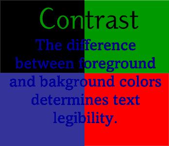
3 Imaging in the TEM What is the contrast? In microscopy, contrast is the difference in intensity between a feature of interest (I s ) and its background (I 0 ). Contrast is usually described as a fraction such as: I I I s 0 C = = 0 I I 0 You won t see anything on the screen or on the photograph, unless the contrast from your specimen exceeds 5-10%.
4


5 In optical micrograph, contrast indicates the grain boundary and grain orientation. In TEM micrograph, contrast indicates many information about the microstructure of specimen

6 Contrast indicates precipitates, dislocations, and thickness variation in Ni- Cr-Ti-Al alloy, Hirsch, Howie, Nicholson, Pashley, Whelan, 1977
7 Intensity and Contrast Intensity and contrast are two different conception. We can have strong or weak contrast but not bright or dark contrast The term bright and dark refer to the intensity, i.e. the density of electrons hitting the screen/detector ( number of electrons /unit area) We usually get the strongest contrast under illumination conditions that lower the overall intensity. By C2 condenser lens, we can adjust the intensity.
8 (a) I (b) I I s High intensity I s High contrast Low intensity Low contrast I 0 I 0 Distance Distance Schematic intensity profiles across an image showing ( a) different intensity levels ( I s and I 0 ), and the difference ( I) between them, which define the contrast. Generally, in a TEM, if the overall intensity is increased (as shown in figure b) the contrast decrease. I I I s 0 C = = 0 I I 0

9 Images and Diffraction Patterns (DP) The uniform electron intensity in incident beam is transformed into a non-uniform intensity after scattering by the specimen as seen in figure. We also know DP shows this nonuniformity A basic procedure to image in the TEM is : first view the DP, since the pattern tells you how your sample is scattering. The relationship between the image and the DP is the most critical for crystalline specimen showing diffraction contrast. You need to view the DP first, whatever contrast mechanism you want to use, and whatever specimen you are studying. Monte Carol simulation of the electron scattering when an incident electron beam passes the specimen The procedure to interpret TEM image usually follows: qualitatively- semi- quantitatively - quantitatively
10 How to obtain TEM images Using the objective aperture to form BF or DF images Using the STEM detector to form BF and DF image HRTEM: usually without aperture To obtain meaningful TEM image Careful preparation of sample. Garbage in, and garbage out Proper setting-up the optics condition Study your materials before TEM session Correct operation of instrument What s your question? Design the lab plan More than one session is necessary Please add more tips from your practice, share and discuss your experience.


11 Incorrect results come from incorrect usage Incorrect Corrected
 of the objective lens, thus blocking out most of the diffraction pattern except that which is")
12 Using the objective aperture to form BF or DF images When we form images in TEM, we either form an image using the central spot, or we use some or all of the scattered electrons. The way we choose which electrons form the image is to insert an aperture into the BFP (back focal plane) of the objective lens, thus blocking out most of the diffraction pattern except that which is visible through the aperture. We use the external drives to move the aperture so that either the direct electrons or some scattered electrons go through it. If the direct beam is selected we call the resultant image a bright-field image (BF image), and if we select scattered electrons of any form, we call it a dark-field image (DF image). Parallel beam condition

13 Center dark field (CDF) image Off-line dark field (ODF) image or dirty dark field image Parallel beam condition


14 Using the STEM detector to form BF and DF image: Convergent beam condition STEM image formation: A Bright Field (BF) detector is placed in a conjugate plane to the back focal plane to intercept the direct beam while a concentric Annular Dark Field (ADF) detector intercepts the diffracted electrons. The signals from either detector are amplified and modulate the STEM CRT. The specimen (Au islands on a C film) gives complementary ADF and BF images as can be seen by clicking the button opposite.
15 In summary, BF and DF images ( for TEM and STEM ) are formed by using the transmitted and diffracted beam respectively. In order to understand and control the contrast in these images, we need to know what features of a specimen cause scattering and what aspects of TEM operation affect the contrast. Mechanism of Contrast for TEM/STEM image 1. Mass-thickness contrast: primary contrast source of TEM/STEM image for noncrystalline materials such as polymers and biological materials. 2. Z-contrast: High resolution STEM image 3. Diffraction contrast: primary contrast source of BF/DF image especially for crystalline materials such as metals. Amplitude of e-wave contributes to the contrast. 4. Phase contrast: High/low resolution TEM image (atomic lattice image). 5. Both the amplitude and the phase contrast: are primary contrast source of electron holography image for magnetic materials 6. In some situations, image contrast may arise from more than one mechanism and one may dominate. 7. Crystalline sample may generate mass-thickness and diffraction contrast when aperture is removed.
16 Mass-thickness Contrast for TEM imaging Mass-thickness contrast arises from incoherent elastic scatter of electron ( Ruthford scattering), which is a strong function of the atomic number Z, i.e. the mass or the density, as well as the thickness of specimen, t. Mass-thickness contrast dominates if the specimen is amorphous. If the specimen is a crystalline, the mass-thickness contrast will compete with the diffraction contrast mechanism. Mechanism is shown in figure Example: stained bacteria sample with constant thickness by microtome prep. The TEM variables affecting the mass-thickness contrast for a given specimen are the objective aperture and the acceleration voltage. Increasing aperture lowers the contrast, and lowering acceleration voltage increases the contrast but reduce the intensity.
17 Less scattering electrons in low mass region More scattering electrons in high mass region Darker contrast Brighter contrast The reverse contrast will be formed in DF imaging mode

18 Impact of Microorganism (e.g. Leptothrix discophora) on the Precipitation and Migration of Metals and Actinides. Samples were sliced into 70 nm by microtome, and then stained using Os, U, and Z etc heavy elements. The contrast are primarily from mass-contrast, since the thickness is constant, 70 nm (Lisa Mullen, former PhD student, HRC).

19 Low kv, 120 kv High kv, 200 kv Small aperture size, 10 µm Large aperture size, 70 µm A smaller aperture enhances the mass-thickness contrast in a similar manner to lowering the kv
20 Mass-thickness Contrast for STEM imaging In a STEM mode, by varying the camera length, L, we change the collection angle of detector. STEM image has more noise and poorer resolution than TEM image, but higher contrast than TEM image. In contrast is more important than resolution, STEM imaging is more useful. STEM imaging is also useful if the specimen is beam sensitive such as some polymers. Examples

21 STEM showing bright contrast of stained bacteria TEM showing dark contrast of stained bacteria
22 Quantitative Mass-thickness Contrast 1. Atom number, Z, is constant, and thickness, t, is varied I Q t C = = 1 e Q t I for t < 1, Q is the total elastic scattering cross section. Since the minimum contrast we can see is ~ 5%, then the minimum t that we can see is t 5 100Q 5A = 100N σρ where A is the atomic weight, N crossection, and ρ is the density 0 0 is Avogadro's number, σ is the single - atom scattering
23 Quantitative Mass-thickness Contrast 2. Atom number, Z, is not constant The atomic scattering factor, f( θ ), f E 1 + E 0 λ ( θ ) = 2 8π a0 θ sin 2 2 ( Z ) f x E: Beam Energy after passing the specimen E0: the beam energy Z: atomic number a0: Bohr radius fx: scattering factor for X-ray ө: scattering angle λ: wavelength The scattering cross section from a σ σ ( β ) 2π f ( θ ) ( β ) = = β a Zλ Z π ( a ) E 1 + E0 β 1+ θ θdθ 2 2 angle β A0: the Bohr radius, Θ0: the characteristic screen angle. Β: the semi-angle of collection of the objective aperture
24 Assume that n electrons are incident on the specimen and dn electron are scattered through an angle > β. Then we can simplify the above equations, ignoring any inelastic scattering. Therefore the reduction in the number of electron going through the objective aperture to form the BF image is given by dn = Nσ n where N = N ln n ( β ) Integrate equation (a) or n = 0 0 = Nσx + ln n n e Nσx So as the specimen mass - thickness (x = ρt) increases, the number of dx / A, N 0 (a) 0 is Avogadro's number, and x = ρt scattered electrons decreases exponentially In principal, the contrast arising from Z and t can be calculated by the above equations. In practice, however, image contrast calculation are not carried out for simple massthickness contrast in materials specimens.
.")
25 Z contrast Z contrast usually refers to STEM high resolution image The image is formed by HAADF (high annular angle dark field) detector as shown in figure Imaging beam condition is always away two-beam condition and close to zone-axis orientation STEM Z-contrast is not equivalent to the TEM Z-contrast image ( mass-thickness contrast). STEM image always contains some diffraction contrast High resolution Z-contrast will be discussed later. Schematic of the HADDF detector set-up for Z-contrast imaging in a STEM. The conventional BF detector is also shown along with the range of electron scattering angle gathered by the detectors Ө2<10 mrad Ө1>50 mrad HADDF BF HADDF


26 Heavy-Ion-Irradiated interface of ZrN TEM STEM Low magnification TEM BF image showing the dislocation loop and interface. The gap of interface with substrate is not very clear due to diffraction contrast In Z-contrast condition, the irradiated interface is very clear.
27 Diffraction contrast Diffraction contrast imaging uses the coherent elastic scattering beam to form image Diffraction contrast imaging is controlled by the Bragg diffraction through variation of crystal structure and orientation of specimen. Diffraction contrast is simply a special form of amplitude contrast because the scattering occurs at Bragg angle. BF and DF image is diffraction contrast image by selecting the direct or diffracted beam as seen figure. Beam condition of diffraction contrast imaging: the incident beam must be parallel in order to give the sharp diffraction spots and thereby strong diffraction contrast. So we need to underfocus C2 to spread the beam. Parallel beam condition
28 Two-beam conditions for diffraction contrast imaging for defects study, especially for metallic materials To get good strong diffraction contrast in both BF and DF image, we usually tilt the specimen to two-beam conditions, in which only one diffracted beam is strong. The direct beam is the other strong spot in the pattern. The electrons in the strongly excited {hkl} beam has been diffracted by a specific set of {hkl} plane. So the area that appears bright in the DF image is the area where {hkl} plane at the Bragg condition. The DF image contains specific orientation information, not just general scattering information as is the case for mass-thickness contrast. Two-beam conditions are not only necessary for good contrast, they also greatly simplify interpretation of image.
29 Diffraction contrast can be primarily used for imaging the crystalline materials including defects. The DP with defects is different than the DP without defects. It is analogous to the 2-D wall structure 2-dimensional arrangements of bricks Brick patterns are represented by commas as motifs showing the difference

30 Two-beam conditions for diffraction contrast imaging BF/DF image pairs along with two-beam diffraction of a series of dislocation and a stacking fault in Cu- 15at%Al.
31 Setting up of the two-beam conditions While looking at the DP, tilt around until only one diffracted beam is strong as shown in figure. The other diffracted beams don t disappear because of the relaxation of the Bragg conditions, but they are relatively faint. In this condition, the contrast might still not be the best (why?). To get the best contrast from defects, the specimen shouldn t be exactly at the Bragg condition (s=0). The specimen should be tilted close to the Bragg condition, and s is small and positive ( the excess {hkl} kikuchi line is just outside the {hkl} spot). Never form strong-beam image with s negative; the defects will be difficult to see.
 DF (c) (a) (a) The [001] zone-axis diffraction patter showing many planes")

 and (c) showing the complementary BF and DF image under two-beam conditions.")
32 (200) (b) (1-11) BF (0-22) (31-1) Only two beams are strong and others are faint due to relaxation of Bragg condition (s) DF (c) (a) (a) The [001] zone-axis diffraction patter showing many planes diffracting with equal strength. In the smaller patterns, the specimen is tilted so there are only two strong beams, the direct [000] on-axis beam and a different one of the {hkl} off-axis diffracted beam. (b) and (c) showing the complementary BF and DF image under two-beam conditions. In (b), the precipitates is diffracted strongly and appears dark. In (c), it appears bright Al-Li Alloy and precipitates
NanoSpective, Inc Progress Drive Suite 137 Orlando, Florida
 TEM Techniques Summary The TEM is an analytical instrument in which a thin membrane (typically < 100nm) is placed in the path of an energetic and highly coherent beam of electrons. Typical operating voltages
Transmission electron Microscopy
 Transmission electron Microscopy Image formation of a concave lens in geometrical optics Some basic features of the transmission electron microscope (TEM) can be understood from by analogy with the operation
Chapter 2 Instrumentation for Analytical Electron Microscopy Lecture 7. Chapter 2 CHEM Fall L. Ma
 Chapter 2 Instrumentation for Analytical Electron Microscopy Lecture 7 Outline Electron Sources (Electron Guns) Thermionic: LaB 6 or W Field emission gun: cold or Schottky Lenses Focusing Aberration Probe
NANO 703-Notes. Chapter 9-The Instrument
 1 Chapter 9-The Instrument Illumination (condenser) system Before (above) the sample, the purpose of electron lenses is to form the beam/probe that will illuminate the sample. Our electron source is macroscopic
ELECTRON MICROSCOPY. 13:10 16:00, Oct. 6, 2008 Institute of Physics, Academia Sinica. Tung Hsu
 ELECTRON MICROSCOPY 13:10 16:00, Oct. 6, 2008 Institute of Physics, Academia Sinica Tung Hsu Department of Materials Science and Engineering National Tsing Hua University Hsinchu 300, TAIWAN Tel. 03-5742564
ELECTRON MICROSCOPY. 14:10 17:00, Apr. 3, 2007 Department of Physics, National Taiwan University. Tung Hsu
 ELECTRON MICROSCOPY 14:10 17:00, Apr. 3, 2007 Department of Physics, National Taiwan University Tung Hsu Department of Materials Science and Engineering National Tsinghua University Hsinchu 300, TAIWAN
Transmission Electron Microscopy 9. The Instrument. Outline
 Transmission Electron Microscopy 9. The Instrument EMA 6518 Spring 2009 02/25/09 Outline The Illumination System The Objective Lens and Stage Forming Diffraction Patterns and Images Alignment and Stigmation
Introduction to Transmission Electron Microscopy (Physical Sciences)
") Introduction to Transmission Electron Microscopy (Physical Sciences) Centre for Advanced Microscopy Program 9:30 10:45 Lecture 1 Basics of TEM 10:45 11:00 Morning tea 11:00 12:15 Lecture 2 Diffraction
Introduction to Transmission Electron Microscopy (Physical Sciences) Centre for Advanced Microscopy Program 9:30 10:45 Lecture 1 Basics of TEM 10:45 11:00 Morning tea 11:00 12:15 Lecture 2 Diffraction
Introduction to Electron Microscopy
 Introduction to Electron Microscopy Prof. David Muller, dm24@cornell.edu Rm 274 Clark Hall, 255-4065 Ernst Ruska and Max Knoll built the first electron microscope in 1931 (Nobel Prize to Ruska in 1986)
MSE 460 TEM Lab 4: Bright/Dark Field Imaging Operation
 MSE 460 TEM Lab 4: Bright/Dark Field Imaging Operation Last updated on 1/8/2018 Jinsong Wu, jinsong-wu@northwestern.edu Aims: The aim of this lab is to familiarize you with bright/dark field imaging operation.
Electron
 Electron 1897: Sir Joseph John Thomson (1856-1940) discovered corpuscles small particles with a charge-to-mass ratio over 1000 times greater than that of protons. Plum pudding model : electrons in a sea
STEM alignment procedures
 STEM alignment procedures Step 1. ASID alignment mode 1. Write down STD for TEM, and then open the ASID control window from dialogue. Also, start Simple imager viewer program on the Desktop. 2. Click on
Chapter 2 The Study of Microbial Structure: Microscopy and Specimen Preparation
 Chapter 2 The Study of Microbial Structure: Microscopy and Specimen Preparation 1 Lenses and the Bending of Light light is refracted (bent) when passing from one medium to another refractive index a measure
GBS765 Hybrid methods
 GBS765 Hybrid methods Lecture 3 Contrast and image formation 10/20/14 4:37 PM The lens ray diagram Magnification M = A/a = v/u and 1/u + 1/v = 1/f where f is the focal length The lens ray diagram So we
ELECTRON MICROSCOPY. 09:10 12:00, Oct. 27, 2006 Institute of Physics, Academia Sinica. Tung Hsu
 ELECTRON MICROSCOPY 09:10 12:00, Oct. 27, 2006 Institute of Physics, Academia Sinica Tung Hsu Department of Materials Science and Engineering National Tsinghua University Hsinchu 300, TAIWAN Tel. 03-5742564
--> Buy True-PDF --> Auto-delivered in 0~10 minutes. JY/T
 Translated English of Chinese Standard: JY/T011-1996 www.chinesestandard.net Sales@ChineseStandard.net INDUSTRY STANDARD OF THE JY PEOPLE S REPUBLIC OF CHINA General rules for transmission electron microscopy
Transmissions Electron Microscopy (TEM)
") Transmissions Electron Microscopy (TEM) Basic principles Diffraction Imaging Specimen preparation A.E. Gunnæs MENA3100 V17 TEM is based on three possible set of techniqes Diffraction From regions down
Transmissions Electron Microscopy (TEM) Basic principles Diffraction Imaging Specimen preparation A.E. Gunnæs MENA3100 V17 TEM is based on three possible set of techniqes Diffraction From regions down
High Resolution Transmission Electron Microscopy (HRTEM) Summary 4/11/2018. Thomas LaGrange Faculty Lecturer and Senior Staff Scientist
 Summary 4/11/2018. Thomas LaGrange Faculty Lecturer and Senior Staff Scientist") Thomas LaGrange Faculty Lecturer and Senior Staff Scientist High Resolution Transmission Electron Microscopy (HRTEM) Doctoral Course MS-637 April 16-18th, 2018 Summary Contrast in TEM images results from
Thomas LaGrange Faculty Lecturer and Senior Staff Scientist High Resolution Transmission Electron Microscopy (HRTEM) Doctoral Course MS-637 April 16-18th, 2018 Summary Contrast in TEM images results from
Chapter 1. Basic Electron Optics (Lecture 2)
") Chapter 1. Basic Electron Optics (Lecture 2) Basic concepts of microscope (Cont ) Fundamental properties of electrons Electron Scattering Instrumentation Basic conceptions of microscope (Cont ) Ray diagram
Chapter 1. Basic Electron Optics (Lecture 2) Basic concepts of microscope (Cont ) Fundamental properties of electrons Electron Scattering Instrumentation Basic conceptions of microscope (Cont ) Ray diagram
FYS 4340/FYS Diffraction Methods & Electron Microscopy. Lecture 9. Imaging Part I. Sandeep Gorantla. FYS 4340/9340 course Autumn
 FYS 4340/FYS 9340 Diffraction Methods & Electron Microscopy Lecture 9 Imaging Part I Sandeep Gorantla FYS 4340/9340 course Autumn 2016 1 Imaging 2 Abbe s principle of imaging Unlike with visible light,
Nanotechnology in Consumer Products
 Nanotechnology in Consumer Products Advances in Transmission Electron Microscopy Friday, April 21, 2017 October 31, 2014 The webinar will begin at 1pm Eastern Time Click here to watch the webinar recording
A few concepts in TEM and STEM explained
 A few concepts in TEM and STEM explained Martin Ek November 23, 2011 1 Introduction This is a collection of short, qualitative explanations of key concepts in TEM and STEM. Most of them are beyond what
TEM theory Basic optics, image formation and key elements
 Workshop series of Chinese 3DEM community Get acquainted with Cryo-Electron Microscopy: First Chinese Workshop for Structural Biologists TEM theory Basic optics, image formation and key elements Jianlin
Low-energy Electron Diffractive Imaging for Three dimensional Light-element Materials
 Low-energy Electron Diffractive Imaging for Three dimensional Light-element Materials Hitachi Review Vol. 61 (2012), No. 6 269 Osamu Kamimura, Ph. D. Takashi Dobashi OVERVIEW: Hitachi has been developing
Indiana University JEM-3200FS
 Indiana University JEM-3200FS Installation Specification Model: JEM 3200FS Serial Number: EM 15000013 Objective Lens Configuration: High Resolution Pole Piece (HRP) JEOL Engineer: Michael P. Van Etten
Development of JEM-2800 High Throughput Electron Microscope
 Development of JEM-2800 High Throughput Electron Microscope Mitsuhide Matsushita, Shuji Kawai, Takeshi Iwama, Katsuhiro Tanaka, Toshiko Kuba and Noriaki Endo EM Business Unit, JEOL Ltd. Electron Optics
CHAPTER TWO METALLOGRAPHY & MICROSCOPY
 CHAPTER TWO METALLOGRAPHY & MICROSCOPY 1. INTRODUCTION: Materials characterisation has two main aspects: Accurately measuring the physical, mechanical and chemical properties of materials Accurately measuring
Basics of Light Microscopy and Metallography
 ENGR45: Introduction to Materials Spring 2012 Laboratory 8 Basics of Light Microscopy and Metallography In this exercise you will: gain familiarity with the proper use of a research-grade light microscope
VISUAL PHYSICS ONLINE DEPTH STUDY: ELECTRON MICROSCOPES
 VISUAL PHYSICS ONLINE DEPTH STUDY: ELECTRON MICROSCOPES Shortly after the experimental confirmation of the wave properties of the electron, it was suggested that the electron could be used to examine objects
microscopy A great online resource Molecular Expressions, a Microscope Primer Partha Roy
 Fundamentals of optical microscopy A great online resource Molecular Expressions, a Microscope Primer http://micro.magnet.fsu.edu/primer/index.html Partha Roy 1 Why microscopy Topics Functions of a microscope
No part of this material may be reproduced without explicit written permission.
 This material is provided for educational use only. The information in these slides including all data, images and related materials are the property of : Robert M. Glaeser Department of Molecular & Cell
Introduction to Electron Microscopy-II
 Introduction to Electron Microscopy-II Prof. David Muller, dm24@cornell.edu Rm 274 Clark Hall, 255-4065 Ernst Ruska and Max Knoll built the first electron microscope in 1931 (Nobel Prize to Ruska in 1986)
S200 Course LECTURE 1 TEM
 S200 Course LECTURE 1 TEM Development of Electron Microscopy 1897 Discovery of the electron (J.J. Thompson) 1924 Particle and wave theory (L. de Broglie) 1926 Electromagnetic Lens (H. Busch) 1932 Construction
ABC Math Student Copy. N. May ABC Math Student Copy. Physics Week 13(Sem. 2) Name. Light Chapter Summary Cont d 2
 Name. Light Chapter Summary Cont d 2") Page 1 of 12 Physics Week 13(Sem. 2) Name Light Chapter Summary Cont d 2 Lens Abberation Lenses can have two types of abberation, spherical and chromic. Abberation occurs when the rays forming an image
Page 1 of 12 Physics Week 13(Sem. 2) Name Light Chapter Summary Cont d 2 Lens Abberation Lenses can have two types of abberation, spherical and chromic. Abberation occurs when the rays forming an image
Full-screen mode Popup controls. Overview of the microscope user interface, TEM User Interface and TIA on the left and EDS on the right
 Quick Guide to Operating FEI Titan Themis G2 200 (S)TEM: TEM mode Susheng Tan Nanoscale Fabrication and Characterization Facility, University of Pittsburgh Office: M104/B01 Benedum Hall, 412-383-5978,
Observing Microorganisms through a Microscope LIGHT MICROSCOPY: This type of microscope uses visible light to observe specimens. Compound Light Micros
 PHARMACEUTICAL MICROBIOLOGY JIGAR SHAH INSTITUTE OF PHARMACY NIRMA UNIVERSITY Observing Microorganisms through a Microscope LIGHT MICROSCOPY: This type of microscope uses visible light to observe specimens.
(Refer Slide Time: 00:10)
") Fundamentals of optical and scanning electron microscopy Dr. S. Sankaran Department of Metallurgical and Materials Engineering Indian Institute of Technology, Madras Module 03 Unit-6 Instrumental details
Fundamentals of optical and scanning electron microscopy Dr. S. Sankaran Department of Metallurgical and Materials Engineering Indian Institute of Technology, Madras Module 03 Unit-6 Instrumental details
Resolution. Diffraction from apertures limits resolution. Rayleigh criterion θ Rayleigh = 1.22 λ/d 1 peak at 2 nd minimum. θ f D
 Microscopy Outline 1. Resolution and Simple Optical Microscope 2. Contrast enhancement: Dark field, Fluorescence (Chelsea & Peter), Phase Contrast, DIC 3. Newer Methods: Scanning Tunneling microscopy (STM),
1.1. In regular TEM imaging mode, find a region of interest and set it at eucentric height.
 JEOL 2010F operating procedure Covers operation in STEM mode (See separate procedures for operation in TEM mode and operation of EDS system) Nicholas G. Rudawski ngr@ufl.edu (805) 252-4916 NOTE: this operating
Observing Microorganisms through a Microscope
 2016/2/19 PowerPoint Lecture Presentations prepared by Bradley W. Christian, McLennan Community College CHAPTER 3 Observing Microorganisms through a Microscope 1 Figure 3.2 Microscopes and Magnification.
MSE 595T Transmission Electron Microscopy. Laboratory III TEM Imaging - I
 MSE 595T Basic Transmission Electron Microscopy TEM Imaging - I Purpose The purpose of this lab is to: 1. Make fine adjustments to the microscope alignment 2. Obtain a diffraction pattern 3. Obtain an
INTRODUCTION THIN LENSES. Introduction. given by the paraxial refraction equation derived last lecture: Thin lenses (19.1) = 1. Double-lens systems
 = 1. Double-lens systems") Chapter 9 OPTICAL INSTRUMENTS Introduction Thin lenses Double-lens systems Aberrations Camera Human eye Compound microscope Summary INTRODUCTION Knowledge of geometrical optics, diffraction and interference,
Chapter 9 OPTICAL INSTRUMENTS Introduction Thin lenses Double-lens systems Aberrations Camera Human eye Compound microscope Summary INTRODUCTION Knowledge of geometrical optics, diffraction and interference,
MSE 460 TEM Lab 2: Basic Alignment and Operation of Microscope
 MSE 460 TEM Lab 2: Basic Alignment and Operation of Microscope Last updated on 1/8/2018 Jinsong Wu, jinsong-wu@northwestern.edu Aims: The aim of this lab is to familiarize you with basic TEM alignment
Diffraction Single-slit Double-slit Diffraction grating Limit on resolution X-ray diffraction. Phys 2435: Chap. 36, Pg 1
 Diffraction Single-slit Double-slit Diffraction grating Limit on resolution X-ray diffraction Phys 2435: Chap. 36, Pg 1 Single Slit New Topic Phys 2435: Chap. 36, Pg 2 Diffraction: bending of light around
Physics 431 Final Exam Examples (3:00-5:00 pm 12/16/2009) TIME ALLOTTED: 120 MINUTES Name: Signature:
 TIME ALLOTTED: 120 MINUTES Name: Signature:") Physics 431 Final Exam Examples (3:00-5:00 pm 12/16/2009) TIME ALLOTTED: 120 MINUTES Name: PID: Signature: CLOSED BOOK. TWO 8 1/2 X 11 SHEET OF NOTES (double sided is allowed), AND SCIENTIFIC POCKET CALCULATOR
Physics 431 Final Exam Examples (3:00-5:00 pm 12/16/2009) TIME ALLOTTED: 120 MINUTES Name: PID: Signature: CLOSED BOOK. TWO 8 1/2 X 11 SHEET OF NOTES (double sided is allowed), AND SCIENTIFIC POCKET CALCULATOR
Light Microscopy. Upon completion of this lecture, the student should be able to:
 Light Light microscopy is based on the interaction of light and tissue components and can be used to study tissue features. Upon completion of this lecture, the student should be able to: 1- Explain the
UNIVERSITY OF FLORIDA 1978
 THE EFFECT OF CRYSTAL DEFECTS ON MICRODIFFRACTION PATTERNS BY JOHN BEVERLY WARREN A DISSERTATION PRESENTED TO THE GRADUATE COUNCIL OF THE UNIVERSITY OF FLORIDA IN PARTIAL FULFILLMENT OF THE REQUIREMENTS
Fiber Optic Communications
 Fiber Optic Communications ( Chapter 2: Optics Review ) presented by Prof. Kwang-Chun Ho 1 Section 2.4: Numerical Aperture Consider an optical receiver: where the diameter of photodetector surface area
Point Spread Function. Confocal Laser Scanning Microscopy. Confocal Aperture. Optical aberrations. Alternative Scanning Microscopy
 Bi177 Lecture 5 Adding the Third Dimension Wide-field Imaging Point Spread Function Deconvolution Confocal Laser Scanning Microscopy Confocal Aperture Optical aberrations Alternative Scanning Microscopy
EUV Plasma Source with IR Power Recycling
 1 EUV Plasma Source with IR Power Recycling Kenneth C. Johnson kjinnovation@earthlink.net 1/6/2016 (first revision) Abstract Laser power requirements for an EUV laser-produced plasma source can be reduced
Phase plates for cryo-em
 Max Planck Institute of Biochemistry Martinsried, Germany MAX PLANCK SOCIETY Phase plates for cryo-em Rado Danev Max Planck Institute of Biochemistry, Martinsried, Germany. EMBO course 2017, London, UK
Be aware that there is no universal notation for the various quantities.
 Fourier Optics v2.4 Ray tracing is limited in its ability to describe optics because it ignores the wave properties of light. Diffraction is needed to explain image spatial resolution and contrast and
Katarina Logg, Kristofer Bodvard, Mikael Käll. Dept. of Applied Physics. 12 September Optical Microscopy. Supervisor s signature:...
 Katarina Logg, Kristofer Bodvard, Mikael Käll Dept. of Applied Physics 12 September 2007 O1 Optical Microscopy Name:.. Date:... Supervisor s signature:... Introduction Over the past decades, the number
MASSACHUSETTS INSTITUTE OF TECHNOLOGY Mechanical Engineering Department. 2.71/2.710 Final Exam. May 21, Duration: 3 hours (9 am-12 noon)
") MASSACHUSETTS INSTITUTE OF TECHNOLOGY Mechanical Engineering Department 2.71/2.710 Final Exam May 21, 2013 Duration: 3 hours (9 am-12 noon) CLOSED BOOK Total pages: 5 Name: PLEASE RETURN THIS BOOKLET WITH
MASSACHUSETTS INSTITUTE OF TECHNOLOGY Mechanical Engineering Department 2.71/2.710 Final Exam May 21, 2013 Duration: 3 hours (9 am-12 noon) CLOSED BOOK Total pages: 5 Name: PLEASE RETURN THIS BOOKLET WITH
Tutorial on Linear Image Simulations of Phase-Contrast and Incoherent Imaging by convolutions
 Tutorial on Linear Image Simulations of Phase-Contrast and Incoherent Imaging by convolutions Huolin Xin, David Muller, based on Appendix A of Kirkland s book This tutorial covers the use of temcon and
The Wave Nature of Light
 The Wave Nature of Light Physics 102 Lecture 7 4 April 2002 Pick up Grating & Foil & Pin 4 Apr 2002 Physics 102 Lecture 7 1 Light acts like a wave! Last week we saw that light travels from place to place
Using Stock Optics. ECE 5616 Curtis
 Using Stock Optics What shape to use X & Y parameters Please use achromatics Please use camera lens Please use 4F imaging systems Others things Data link Stock Optics Some comments Advantages Time and
Scanning electron microscope
 Scanning electron microscope 6 th CEMM workshop Maja Koblar, Sc. Eng. Physics Outline The basic principle? What is an electron? Parts of the SEM Electron gun Electromagnetic lenses Apertures Chamber and
Fabrication of Probes for High Resolution Optical Microscopy
 Fabrication of Probes for High Resolution Optical Microscopy Physics 564 Applied Optics Professor Andrès La Rosa David Logan May 27, 2010 Abstract Near Field Scanning Optical Microscopy (NSOM) is a technique
Microscopy techniques for biomaterials. Engenharia Biomédica. Patrícia Almeida Carvalho
 Microscopy techniques for biomaterials Engenharia Biomédica Patrícia Almeida Carvalho 1 2 Why microscopy? http://www.cellsalive.com/howbig.htm 3 Why microscopy? Resolution of an optical system Diffraction
Cs-corrector. Felix de Haas
 Cs-corrector. Felix de Haas Content Non corrector systems Lens aberrations and how to minimize? Corrector systems How is it done? Lens aberrations Spherical aberration Astigmatism Coma Chromatic Quality
Lecture 15: Fraunhofer diffraction by a circular aperture
 Lecture 15: Fraunhofer diffraction by a circular aperture Lecture aims to explain: 1. Diffraction problem for a circular aperture 2. Diffraction pattern produced by a circular aperture, Airy rings 3. Importance
Microscopy. Matti Hotokka Department of Physical Chemistry Åbo Akademi University
 Microscopy Matti Hotokka Department of Physical Chemistry Åbo Akademi University What s coming Anatomy of a microscope Modes of illumination Practicalities Special applications Basic microscope Ocular
Microscopy Techniques that make it easy to see things this small.
 Microscopy Techniques that make it easy to see things this small. What is a Microscope? An instrument for viewing objects that are too small to be seen easily by the naked eye. Dutch spectacle-makers Hans
Physics 3340 Spring Fourier Optics
 Physics 3340 Spring 011 Purpose Fourier Optics In this experiment we will show how the Fraunhofer diffraction pattern or spatial Fourier transform of an object can be observed within an optical system.
MASSACHUSETTS INSTITUTE OF TECHNOLOGY. 2.71/2.710 Optics Spring 14 Practice Problems Posted May 11, 2014
 MASSACHUSETTS INSTITUTE OF TECHNOLOGY 2.71/2.710 Optics Spring 14 Practice Problems Posted May 11, 2014 1. (Pedrotti 13-21) A glass plate is sprayed with uniform opaque particles. When a distant point
Diffraction. Interference with more than 2 beams. Diffraction gratings. Diffraction by an aperture. Diffraction of a laser beam
 Diffraction Interference with more than 2 beams 3, 4, 5 beams Large number of beams Diffraction gratings Equation Uses Diffraction by an aperture Huygen s principle again, Fresnel zones, Arago s spot Qualitative
2014 HTD-E with options
 with options The HT7700 : a user-friendly, ergonomic digital TEM with options User-Friendly r end Design Ambient light operation. Multiple automated functions for alignment, focus and stigmation as standard
ECEN 4606, UNDERGRADUATE OPTICS LAB
 ECEN 4606, UNDERGRADUATE OPTICS LAB Lab 2: Imaging 1 the Telescope Original Version: Prof. McLeod SUMMARY: In this lab you will become familiar with the use of one or more lenses to create images of distant
Image Formation. Light from distant things. Geometrical optics. Pinhole camera. Chapter 36
 Light from distant things Chapter 36 We learn about a distant thing from the light it generates or redirects. The lenses in our eyes create images of objects our brains can process. This chapter concerns
MODULE I SCANNING ELECTRON MICROSCOPE (SEM)
") MODULE I SCANNING ELECTRON MICROSCOPE (SEM) Scanning Electron Microscope (SEM) Initially, the plan of SEM was offered by H. Stintzing in 1927 (a German patent application). His suggested procedure was
MODULE I SCANNING ELECTRON MICROSCOPE (SEM) Scanning Electron Microscope (SEM) Initially, the plan of SEM was offered by H. Stintzing in 1927 (a German patent application). His suggested procedure was
Advanced Materials Characterization Workshop
 University of Illinois at Urbana-Champaign Materials Research Laboratory Advanced Materials Characterization Workshop June 3 rd and 4 th, 2013 Transmission Electron Microscopy Wacek Swiech, Honghui Zhou,
EE119 Introduction to Optical Engineering Spring 2003 Final Exam. Name:
 EE119 Introduction to Optical Engineering Spring 2003 Final Exam Name: SID: CLOSED BOOK. THREE 8 1/2 X 11 SHEETS OF NOTES, AND SCIENTIFIC POCKET CALCULATOR PERMITTED. TIME ALLOTTED: 180 MINUTES Fundamental
FRAUNHOFER AND FRESNEL DIFFRACTION IN ONE DIMENSION
 FRAUNHOFER AND FRESNEL DIFFRACTION IN ONE DIMENSION Revised November 15, 2017 INTRODUCTION The simplest and most commonly described examples of diffraction and interference from two-dimensional apertures
Lecture Notes 10 Image Sensor Optics. Imaging optics. Pixel optics. Microlens
 Lecture Notes 10 Image Sensor Optics Imaging optics Space-invariant model Space-varying model Pixel optics Transmission Vignetting Microlens EE 392B: Image Sensor Optics 10-1 Image Sensor Optics Microlens
Diffractive Axicon application note
 Diffractive Axicon application note. Introduction 2. General definition 3. General specifications of Diffractive Axicons 4. Typical applications 5. Advantages of the Diffractive Axicon 6. Principle of
Nanotechnology and material science Lecture V
 Most widely used nanoscale microscopy. Based on possibility to create bright electron beam with sub-nm spot size. History: Ernst Ruska (1931), Nobel Prize (1986) For visible light λ=400-700nm, for electrons
SECONDARY ELECTRON DETECTION
 SECONDARY ELECTRON DETECTION CAMTEC Workshop Presentation Haitian Xu June 14 th 2010 Introduction SEM Raster scan specimen surface with focused high energy e- beam Signal produced by beam interaction with
Chapter 36: diffraction
 Chapter 36: diffraction Fresnel and Fraunhofer diffraction Diffraction from a single slit Intensity in the single slit pattern Multiple slits The Diffraction grating X-ray diffraction Circular apertures
Introduction: Why electrons?
 Introduction: Why electrons? 1 Radiations Visible light X-rays Electrons Neutrons Advantages Not very damaging Easily focused Eye wonderful detector Small wavelength (Angstroms) Good penetration Small
1 Diffraction of Microwaves
 1 Diffraction of Microwaves 1.1 Purpose In this lab you will investigate the coherent scattering of electromagnetic waves from a periodic structure. The experiment is a direct analog of the Bragg diffraction
Why is There a Black Dot when Defocus = 1λ?
 Why is There a Black Dot when Defocus = 1λ? W = W 020 = a 020 ρ 2 When a 020 = 1λ Sag of the wavefront at full aperture (ρ = 1) = 1λ Sag of the wavefront at ρ = 0.707 = 0.5λ Area of the pupil from ρ =
Laser Telemetric System (Metrology)
") Laser Telemetric System (Metrology) Laser telemetric system is a non-contact gauge that measures with a collimated laser beam (Refer Fig. 10.26). It measure at the rate of 150 scans per second. It basically
Laser Telemetric System (Metrology) Laser telemetric system is a non-contact gauge that measures with a collimated laser beam (Refer Fig. 10.26). It measure at the rate of 150 scans per second. It basically
JEM-F200. Multi-purpose Electron Microscope. Scientific / Metrology Instruments Multi-purpose Electron Microscope
 Scientific / Metrology Instruments Multi-purpose Electron Microscope JEM-F200 Multi-purpose Electron Microscope JEM-F200/F2 is a multi-purpose electron microscope of the new generation to meet today's
Low Voltage Electron Microscope
 LVEM5 Low Voltage Electron Microscope Nanoscale from your benchtop LVEM5 Delong America DELONG INSTRUMENTS COMPACT BUT POWERFUL The LVEM5 is designed to excel across a broad range of applications in material
Test procedures Page: 1 of 5
 Test procedures Page: 1 of 5 1 Scope This part of document establishes uniform requirements for measuring the numerical aperture of optical fibre, thereby assisting in the inspection of fibres and cables
NAME SECTION PERFORMANCE TASK # 3. Part I. Qualitative Relationships
 NAME SECTION PARTNERS DATE PERFORMANCE TASK # 3 You must work in teams of three or four (ask instructor) and will turn in ONE report. Answer all questions. Write in complete sentences. You must hand this
Tecnai on-line help manual --
 Tecnai on-line help Alignments 1 Tecnai on-line help manual -- Alignments Table of Contents 1 Alignments in the Tecnai microscope...5 2 Alignment procedures...6 3 Introduction to electron optics...11 3.1
TA/TI survey. Phy Phy
 TA/TI survey https://webapps.pas.rochester.edu/secure/phpq/ Phy121 7 60 73 81 Phy123 1 6 11 18 Chapter 35 Diffraction and Polarization Double- Slit Experiment destructive interference Two sources of light
SUPPLEMENTARY INFORMATION
 Optically reconfigurable metasurfaces and photonic devices based on phase change materials S1: Schematic diagram of the experimental setup. A Ti-Sapphire femtosecond laser (Coherent Chameleon Vision S)
p q p f f f q f p q f NANO 703-Notes Chapter 5-Magnification and Electron Sources
 Chapter 5-agnification and Electron Sources Lens equation Let s first consider the properties of an ideal lens. We want rays diverging from a point on an object in front of the lens to converge to a corresponding
Biology 29 Cell Structure and Function Spring, 2009 Springer LABORATORY 1: THE LIGHT MICROSCOPE
 Biology 29 Cell Structure and Function Spring, 2009 Springer LABORATORY 1: THE LIGHT MICROSCOPE Prior to lab: 1) Read these instructions (p 1-6) 2) Go through the online tutorial, the microscopy pre-lab
Atomic Resolution Imaging with a sub-50 pm Electron Probe
 Atomic Resolution Imaging with a sub-50 pm Electron Probe Rolf Erni, Marta D. Rossell, Christian Kisielowski, Ulrich Dahmen National Center for Electron Microscopy, Lawrence Berkeley National Laboratory
Chapter Ray and Wave Optics
 109 Chapter Ray and Wave Optics 1. An astronomical telescope has a large aperture to [2002] reduce spherical aberration have high resolution increase span of observation have low dispersion. 2. If two
Introduction of New Products
 Field Emission Electron Microscope JEM-3100F For evaluation of materials in the fields of nanoscience and nanomaterials science, TEM is required to provide resolution and analytical capabilities that can
Measurement of Surface Profile and Layer Cross-section with Wide Field of View and High Precision
 Hitachi Review Vol. 65 (2016), No. 7 243 Featured Articles Measurement of Surface Profile and Layer Cross-section with Wide Field of View and High Precision VS1000 Series Coherence Scanning Interferometer
ELECTRON MICROSCOPY AN OVERVIEW
 ELECTRON MICROSCOPY AN OVERVIEW Anjali Priya 1, Abhishek Singh 2, Nikhil Anand Srivastava 3 1,2,3 Department of Electrical & Instrumentation, Sant Longowal Institute of Engg. & Technology, Sangrur, India.
Medical Imaging. X-rays, CT/CAT scans, Ultrasound, Magnetic Resonance Imaging
 Medical Imaging X-rays, CT/CAT scans, Ultrasound, Magnetic Resonance Imaging From: Physics for the IB Diploma Coursebook 6th Edition by Tsokos, Hoeben and Headlee And Higher Level Physics 2 nd Edition
Scanning Electron Microscopy. EMSE-515 F. Ernst
 Scanning Electron Microscopy EMSE-515 F. Ernst 1 2 Scanning Electron Microscopy Max Knoll Manfred von Ardenne Manfred von Ardenne Principle of Scanning Electron Microscopy 3 Principle of Scanning Electron