Functions of the SEM subsystems
|
|
|
- Randolf Simpson
- 5 years ago
- Views:
Transcription
1 Functions of the SEM subsystems Electronic column It consists of an electron gun and two or more electron lenses, which influence the path of electrons traveling down an evacuated tube. The base of the column is usually taken up with vacuum pumps that produce a vacuum of about 10-4 Pa Control console It consists of a computer system with a viewing screen and knobs and keyboard to control the electron beam
2 Electron gun The electron gun generates electrons and accelerates them to an energy in the range KeV. Electromagnetic lenses Since the spot size from the source (tungsten hairpin gun) is too large to produce a sharp image, lenses are used to demagnify it. The beam emerges from the final lens with a spot size that could be also less than 10 nm. Deflection system The scanned image is formed point by point. The deflection system causes the beam to move to a series of discrete locations along a line and then along another line below the first, and so on, until a rectangular raster is generated on the specimen. Simultaneously, a similar raster is created on the viewing screen.
3 Electron detectors Contrast in an image arises when the signal collected from the beam-specimen interaction varies from one location to another. When the electron beam impinges on the specimen, many types of signals are generated and any of them can be displayed as an image. The electronics of the detector system converts the signals to point-by-point intensity changes on the viewing screen and produces an image. The two signals most often used to produce SEM images are secondary electrons (SE) and backscattered electrons (BSE). Sometimes X-ray analyses are performed simultaneously in order to have compositional information about the specimen.
4 Parameters characterizing a SEM micrograph Images can provide much more information about a specimen if we understand the conditions under where they are taken.the limiting sharpness and feature visibility of SEM micrographs are dependent upon four parameters d p electron probe size i p electron probe current а p electron probe convergence angle V 0 electron beam accelerating voltage (in kv) d p i p а p V 0 the spot size is defined as the diameter of the final beam at the surface of the specimen the probe current is the current that impinges upon the specimen and generates the various imaging signals the convergence angle is the half-angle of the cone of the electrons converging onto the specimen electron beam accelerating voltage is the accelerating voltage of the electron gun
5 Each of these four beam parameters dominates one of the four major SEM imaging mode d p i p а p V 0 resolution mode high-current mode depth-of-focus mode low voltage mode
6 Resolution mode For the highest resolution image d p must be as small as possible while at the same time containg sufficient current to exceed the visibility threshold for the contrast produced by the features of interest. Resolution refers to the finest details that can be observed. To image the finest details of the specimen surface, the probe diameter must be comparable with or smaller than the feature itself. High current mode For the best image visibility and quality, large beam currents i p are required. Unless the contrast between an image feature and the background is distinguishable above random signal fluctuactions (noise), details cannot be observed even if the spot size is small enough fot it to be easily resolved. Moreover, large beam currents are necessary for X-ray microanalysis because only a small fraction of beam interactions result in X-ray emission.
7 Resolution Small spot-size Large spot-size
8 Depth of- focus mode For the best depth of focus а p must be as small as possible. By making the beam convergence angle low, the beam diameter changes only a little over a long vertical distance and so feature on the surface at different heights will appear to be in focus at the same time. For large beam convergence angle details at different heights will be out of focus and no surface details can be seen. The large depth of focus of the SEM is one of the its greatest strengths. Low voltage mode At low accelerating voltages ( 5 kv), the beam interaction with the specimen is confined to regions very close to the surface. This provides an image which is rich in surface details compared to those obtained at higher accelerating voltages (10-15 kv).
Scanning electron microscope
 Scanning electron microscope 5 th CEMM workshop Maja Koblar, Sc. Eng. Physics Outline The basic principle? What is an electron? Parts of the SEM Electron gun Electromagnetic lenses Apertures Detectors
Scanning Electron Microscopy. EMSE-515 F. Ernst
 Scanning Electron Microscopy EMSE-515 F. Ernst 1 2 Scanning Electron Microscopy Max Knoll Manfred von Ardenne Manfred von Ardenne Principle of Scanning Electron Microscopy 3 Principle of Scanning Electron
Introduction to Scanning Electron Microscopy
 Introduction to Scanning Electron Microscopy By: Brandon Cheney Ant s Leg Integrated Circuit Nano-composite This document was created as part of a Senior Project in the Materials Engineering Department
Scanning electron microscope
 Scanning electron microscope 6 th CEMM workshop Maja Koblar, Sc. Eng. Physics Outline The basic principle? What is an electron? Parts of the SEM Electron gun Electromagnetic lenses Apertures Chamber and
Scanning Electron Microscopy SEM. Warren Straszheim, PhD MARL, 23 Town Engineering
 Scanning Electron Microscopy SEM Warren Straszheim, PhD MARL, 23 Town Engineering wesaia@iastate.edu 515-294-8187 How it works Create a focused electron beam Accelerate it Scan it across the sample Map
SECONDARY ELECTRON DETECTION
 SECONDARY ELECTRON DETECTION CAMTEC Workshop Presentation Haitian Xu June 14 th 2010 Introduction SEM Raster scan specimen surface with focused high energy e- beam Signal produced by beam interaction with
MODULE I SCANNING ELECTRON MICROSCOPE (SEM)
") MODULE I SCANNING ELECTRON MICROSCOPE (SEM) Scanning Electron Microscope (SEM) Initially, the plan of SEM was offered by H. Stintzing in 1927 (a German patent application). His suggested procedure was
MODULE I SCANNING ELECTRON MICROSCOPE (SEM) Scanning Electron Microscope (SEM) Initially, the plan of SEM was offered by H. Stintzing in 1927 (a German patent application). His suggested procedure was
S200 Course LECTURE 1 TEM
 S200 Course LECTURE 1 TEM Development of Electron Microscopy 1897 Discovery of the electron (J.J. Thompson) 1924 Particle and wave theory (L. de Broglie) 1926 Electromagnetic Lens (H. Busch) 1932 Construction
Scanning Electron Microscopy Basics and Applications
 Scanning Electron Microscopy Basics and Applications Dr. Julia Deuschle Stuttgart Center for Electron Microscopy MPI for Solid State Research Room: 1E15, phone: 0711/ 689-1193 email: j.deuschle@fkf.mpg.de
ELECTRON MICROSCOPY AN OVERVIEW
 ELECTRON MICROSCOPY AN OVERVIEW Anjali Priya 1, Abhishek Singh 2, Nikhil Anand Srivastava 3 1,2,3 Department of Electrical & Instrumentation, Sant Longowal Institute of Engg. & Technology, Sangrur, India.
(Refer Slide Time: 00:10)
") Fundamentals of optical and scanning electron microscopy Dr. S. Sankaran Department of Metallurgical and Materials Engineering Indian Institute of Technology, Madras Module 03 Unit-6 Instrumental details
Fundamentals of optical and scanning electron microscopy Dr. S. Sankaran Department of Metallurgical and Materials Engineering Indian Institute of Technology, Madras Module 03 Unit-6 Instrumental details
Topics 3b,c Electron Microscopy
 Topics 3b,c Electron Microscopy 1.0 Introduction and History 1.1 Characteristic Information 2.0 Basic Principles 2.1 Electron-Solid Interactions 2.2 Electromagnetic Lenses 2.3 Breakdown of an Electron
SCANNING ELECTRON MICROSCOPY AND X-RAY MICROANALYSIS
 SCANNING ELECTRON MICROSCOPY AND X-RAY MICROANALYSIS Robert Edward Lee Electron Microscopy Center Department of Anatomy and Neurobiology Colorado State University P T R Prentice Hall, Englewood Cliffs,
Secondary Electron Detector
 Secondary Electron Detector Fig. 17 Everhart-Thornley Detector (Fig. 7-9, p. 215, Bozzola and Russell) Secondary electrons (SE) are attracted to Faraday cage because of its positive charge. Detector surface
OPERATION OF THE HITACHI S-450 SCANNING ELECTRON MICROSCOPE. by Doug Bray Department of Biological Sciences University of Lethbridge
 OPERATION OF THE HITACHI S-450 SCANNING ELECTRON MICROSCOPE by Doug Bray Department of Biological Sciences University of Lethbridge Revised September, 2000 Note: The terms in bold in this document represent
Scanning Electron Microscopy
 Scanning Electron Microscopy For the semiconductor industry A tutorial Titel Vorname Nachname Titel Jobtitle, Bereich/Abteilung Overview Scanning Electron microscopy Scanning Electron Microscopy (SEM)
Scanning Electron Microscope in Our Facility
 SEM Training Scanning Electron Microscope in Our Facility Specifications Table SEM ESEM FE-SEM-F FE-SEM-J FE-SEM-H FE-SEM-CZ Device name TM3030 Inspect S50 Inspect F50 JSM-7600 S-4700 Marlin compact Company
Transmission Electron Microscopy 9. The Instrument. Outline
 Transmission Electron Microscopy 9. The Instrument EMA 6518 Spring 2009 02/25/09 Outline The Illumination System The Objective Lens and Stage Forming Diffraction Patterns and Images Alignment and Stigmation
STRUCTURE OF THE MICROSCOPE
 STRUCTURE OF THE MICROSCOPE Use the word list to label the microscope below: Light Source Coarse adjustment knob Diaphragm Stage Clips Objectives Fine Adjustment Knob Base Stage Stage Clips Arm Revolving
Using the Hitachi 3400-N VP-SEM
 Using the Hitachi 3400-N VP-SEM Opening the Chamber to Load Specimens (This may also be done later using the software) 1. Click the AIR button on the front of the machine: 2. Wait a few minutes until you
ZEISS EVO SOP. May 2017 ELECTRON OPTICS
 ZEISS EVO SOP May 2017 ELECTRON OPTICS The patented EVO column is the area of the SEM, where electrons are emitted, accelerated, deflected, focused, and scanned. Main characteristics of the EVO optics
The light microscope
 What is a microscope? The microscope is an essential tool in modern biology. It allows us to view structural details of organs, tissue, and cells not visible to the naked eye. The microscope should always
p q p f f f q f p q f NANO 703-Notes Chapter 5-Magnification and Electron Sources
 Chapter 5-agnification and Electron Sources Lens equation Let s first consider the properties of an ideal lens. We want rays diverging from a point on an object in front of the lens to converge to a corresponding
SCIENTIFIC INSTRUMENT NEWS. Introduction. Design of the FlexSEM 1000
 SCIENTIFIC INSTRUMENT NEWS 2017 Vol. 9 SEPTEMBER Technical magazine of Electron Microscope and Analytical Instruments. Technical Explanation The FlexSEM 1000: A Scanning Electron Microscope Specializing
Introduction of New Products
 Field Emission Electron Microscope JEM-3100F For evaluation of materials in the fields of nanoscience and nanomaterials science, TEM is required to provide resolution and analytical capabilities that can
2.Components of an electron microscope. a) vacuum systems, b) electron guns, c) electron optics, d) detectors. Marco Cantoni 021/
 vacuum systems, b) electron guns, c) electron optics, d) detectors. Marco Cantoni 021/") 2.Components of an electron microscope a) vacuum systems, b) electron guns, c) electron optics, d) detectors, 021/693.48.16 Centre Interdisciplinaire de Microscopie Electronique CIME Summary Electron propagation
2.Components of an electron microscope a) vacuum systems, b) electron guns, c) electron optics, d) detectors, 021/693.48.16 Centre Interdisciplinaire de Microscopie Electronique CIME Summary Electron propagation
A Portable Scanning Electron Microscope Column Design Based on the Use of Permanent Magnets
 SCANNING VOL. 20, 87 91 (1998) Received October 8, 1997 FAMS, Inc. Accepted with revision November 9, 1997 A Portable Scanning Electron Microscope Column Design Based on the Use of Permanent Magnets A.
Module 4B7: VLSI Design, Technology, and CAD. Scanning Electron Microscopical Examination of CMOS Integrated Circuit
 Engineering Tripos Part IIB FOURTH YEAR Module 4B7: VLSI Design, Technology, and CAD Laboratory Experiment Dr D Holburn and Mr B Breton Scanning Electron Microscopical Examination of CMOS Integrated Circuit
JEOL 6500 User Manual
 LOG IN to your session on the computer to the left of the microscope. Starting Conditions 1. Press Ctrl-Alt-Del and log on to the microscope computer. Click on JEOL PC SEM 6500 icon. Click yes if message
NANO 703-Notes. Chapter 9-The Instrument
 1 Chapter 9-The Instrument Illumination (condenser) system Before (above) the sample, the purpose of electron lenses is to form the beam/probe that will illuminate the sample. Our electron source is macroscopic
!"#$$%$&'()*"+,-$'.%",-/"-0*'-$'#'12%0'
*+,-$'.%,-/-0*'-$'#'12%0'") !#$$%$&'()*+,-$'.%,-/-0*'-$'#'12%0' #$%&'()*+!#$%&'()*+,'-+%./%0123453%6%$3+*.-.,27%#.3%$-8'9'37%$%:;;:
!#$$%$&'()*+,-$'.%,-/-0*'-$'#'12%0' #$%&'()*+!#$%&'()*+,'-+%./%0123453%6%$3+*.-.,27%#.3%$-8'9'37%$%:;;:
Electron Sources, Optics and Detectors
 Thomas LaGrange, Ph.D. Faculty Lecturer and Senior Staff Scientist Electron Sources, Optics and Detectors TEM Doctoral Course MS-637 April 16 th -18 th, 2018 Summary Electron propagation is only possible
Quick and simple installation and no maintenance needed. 3 Times More affordable Than a normal SEM. Obtaining results in less than 4 minutes
 INTRODUCTION We believe that every laboratory working in the field of nanotechnology needs an SEM, therefore we would like to introduce to you our IEM series of SEM. In short space of time, our device
Fabrication of Probes for High Resolution Optical Microscopy
 Fabrication of Probes for High Resolution Optical Microscopy Physics 564 Applied Optics Professor Andrès La Rosa David Logan May 27, 2010 Abstract Near Field Scanning Optical Microscopy (NSOM) is a technique
INTRODUCTION We believe that every laboratory working in the field of nanotechnology needs an SEM, therefore we would like to introduce to you our IEM
 INTRODUCTION We believe that every laboratory working in the field of nanotechnology needs an SEM, therefore we would like to introduce to you our IEM series of SEM. In short space of time, our device
Schottky Emission VP FE-SEM
 Schottky Emission VP FE-SEM Variable Pressure The Scanning Electron Microscope (SEM) has played an important role for many years for research and development of advanced materials in the leading edge of
Low Voltage Electron Microscope
 LVEM5 Low Voltage Electron Microscope Nanoscale from your benchtop LVEM5 Delong America DELONG INSTRUMENTS COMPACT BUT POWERFUL The LVEM5 is designed to excel across a broad range of applications in material
How to choose a Scanning Electron Microscope (SEM)
") www.lambdaphoto.co.uk E-guide How to choose a Scanning Electron Microscope (SEM) Providing guidance in the selection of the right microscope for your research Distribution in the UK & Ireland Table of
www.lambdaphoto.co.uk E-guide How to choose a Scanning Electron Microscope (SEM) Providing guidance in the selection of the right microscope for your research Distribution in the UK & Ireland Table of
Oct. 30th- Nov. 1st, 2017
 Thomas LaGrange, Ph.D. Faculty Lecturer and Senior Staff Scientist Electron Sources, Optics and Detectors SEM Doctoral Course MS-636 Oct. 30th- Nov. 1st, 2017 Summary Electron propagation is only possible
Title: Amray 1830 SEM#2 Semiconductor & Microsystems Fabrication Laboratory Revision: D Rev Date: 03/18/2016
 Approved by: Process Engineer / / / / Equipment Engineer 1 SCOPE The purpose of this document is to detail the use of the Amray 1830 SEM. All users are expected to have read and understood this document.
Introduction: Why electrons?
 Introduction: Why electrons? 1 Radiations Visible light X-rays Electrons Neutrons Advantages Not very damaging Easily focused Eye wonderful detector Small wavelength (Angstroms) Good penetration Small
ELECTRON MICROSCOPY. 14:10 17:00, Apr. 3, 2007 Department of Physics, National Taiwan University. Tung Hsu
 ELECTRON MICROSCOPY 14:10 17:00, Apr. 3, 2007 Department of Physics, National Taiwan University Tung Hsu Department of Materials Science and Engineering National Tsinghua University Hsinchu 300, TAIWAN
NanoSpective, Inc Progress Drive Suite 137 Orlando, Florida
 TEM Techniques Summary The TEM is an analytical instrument in which a thin membrane (typically < 100nm) is placed in the path of an energetic and highly coherent beam of electrons. Typical operating voltages
Model SU3500 Scanning Electron Microscope
 Model SU3500 Scanning Electron Microscope Modified and Parts taken from Hitachi Easy Operation Guide. Before using the Model SU3500 SEM, be sure to read the [GENERAL SAFETY GUIDELINES] in the instruction
VISUAL PHYSICS ONLINE DEPTH STUDY: ELECTRON MICROSCOPES
 VISUAL PHYSICS ONLINE DEPTH STUDY: ELECTRON MICROSCOPES Shortly after the experimental confirmation of the wave properties of the electron, it was suggested that the electron could be used to examine objects
2.Components of an electron microscope. a) vacuum systems, b) electron guns, c) electron optics, d) detectors. Marco Cantoni, 021/
 vacuum systems, b) electron guns, c) electron optics, d) detectors. Marco Cantoni, 021/") 2.Components of an electron microscope a) vacuum systems, b) electron guns, c) electron optics, d) detectors Marco Cantoni, 021/693.48.16 Centre Interdisciplinaire de Microscopie Electronique CIME MSE-603
2.Components of an electron microscope a) vacuum systems, b) electron guns, c) electron optics, d) detectors Marco Cantoni, 021/693.48.16 Centre Interdisciplinaire de Microscopie Electronique CIME MSE-603
Scanning Electron Microscope. Instructions for Use
 Scanning Electron Microscope Instructions for Use The reproduction, transmission or use of this document or its contents is not permitted without express written authority. Offenders are liable for damages.
Standard Operating Procedure for the Amray 1810 Scanning Electron Microscope Version: 29 NOVEMBER 2014
 Standard Operating Procedure for the Amray 1810 Scanning Electron Microscope Version: 29 NOVEMBER 2014 1. Utility Requirements a. System power is supplied by two 120 VAC/20 A circuits. When doing maintenance
Oct. 30th- Nov. 1st, 2017
 Thomas LaGrange, Ph.D. Faculty Lecturer and Senior Staff Scientist Electron Sources, Optics and Detectors SEM Doctoral Course MS-636 Oct. 30th- Nov. 1st, 2017 Summary Electron propagation is only possible
Dickinson College Department of Geology
 Dickinson College Department of Geology Title: Equipment: BASIC OPERATION OF THE SCANNING ELECTRON MICROSCOPE (SEM) JEOL JSM-5900 SCANNING ELECTRON MICROSCOPE Revision: 2.2 Effective Date: 1/29/2003 Author(s):
Design and fabrication of a scanning electron microscope using a finite element analysis for electron optical system
 Journal of Mechanical Science and Technology 22 (2008) 1734~1746 Journal of Mechanical Science and Technology www.springerlink.com/content/1738-494x DOI 10.1007/s12206-008-0317-9 Design and fabrication
2. Raise HT to 200kVby following the procedure explained in 1.6.
 JEOL 2100 MANUAL Quick check list 1. If needed, fill the reservoir with LN2 2. Raise HT to 200kVby following the procedure explained in 1.6. 3. Insert specimen holder into TEM (Insert holder in airlock,
ELECTRON MICROSCOPY. 13:10 16:00, Oct. 6, 2008 Institute of Physics, Academia Sinica. Tung Hsu
 ELECTRON MICROSCOPY 13:10 16:00, Oct. 6, 2008 Institute of Physics, Academia Sinica Tung Hsu Department of Materials Science and Engineering National Tsing Hua University Hsinchu 300, TAIWAN Tel. 03-5742564
Observing Microorganisms through a Microscope LIGHT MICROSCOPY: This type of microscope uses visible light to observe specimens. Compound Light Micros
 PHARMACEUTICAL MICROBIOLOGY JIGAR SHAH INSTITUTE OF PHARMACY NIRMA UNIVERSITY Observing Microorganisms through a Microscope LIGHT MICROSCOPY: This type of microscope uses visible light to observe specimens.
Low Voltage Electron Microscope. Nanoscale from your benchtop LVEM5. Delong America
 LVEM5 Low Voltage Electron Microscope Nanoscale from your benchtop LVEM5 Delong America DELONG INSTRUMENTS COMPACT BUT POWERFUL The LVEM5 is designed to excel across a broad range of applications in material
1.1. Log on to the TUMI system (you cannot proceed further until this is done).
.") FEI DB235 SEM mode operation Nicholas G. Rudawski ngr@ufl.edu (805) 252-4916 1. Sample loading 1.1. Log on to the TUMI system (you cannot proceed further until this is done). 1.2. The FIB software (xp)
FEI DB235 SEM mode operation Nicholas G. Rudawski ngr@ufl.edu (805) 252-4916 1. Sample loading 1.1. Log on to the TUMI system (you cannot proceed further until this is done). 1.2. The FIB software (xp)
MICROSCOPE LAB. Resolving Power How well specimen detail is preserved during the magnifying process.
 AP BIOLOGY Cells ACTIVITY #2 MICROSCOPE LAB OBJECTIVES 1. Demonstrate proper care and use of a compound microscope. 2. Identify the parts of the microscope and describe the function of each part. 3. Compare
CPSC 4040/6040 Computer Graphics Images. Joshua Levine
 CPSC 4040/6040 Computer Graphics Images Joshua Levine levinej@clemson.edu Lecture 04 Displays and Optics Sept. 1, 2015 Slide Credits: Kenny A. Hunt Don House Torsten Möller Hanspeter Pfister Agenda Open
NeoScope. Simple Operation to 40,000. Table Top SEM. Serving Advanced Technology
 Table Top SEM Simple Operation to 40,000 Serving Advanced Technology From 10 to 40,000 Table Top SEM Notebook PC version Just plug it to a wall outlet after placing it on a table Desktop PC version Option
5. The Scanning Electron Microscope
 Physical Principles of Electron Microscopy 5. The Scanning Electron Microscope Ray Egerton University of Alberta and National Institute of Nanotechnology Edmonton, Canada www.tem-eels.ca regerton@ualberta.ca
JEM-F200. Multi-purpose Electron Microscope. Scientific / Metrology Instruments Multi-purpose Electron Microscope
 Scientific / Metrology Instruments Multi-purpose Electron Microscope JEM-F200 Multi-purpose Electron Microscope JEM-F200/F2 is a multi-purpose electron microscope of the new generation to meet today's
SEM OPERATION IN LOW VACUUM MODE
 SEM OPERATION IN LOW VACUUM MODE Instructions for JEOL 5800 LV The EVAC light of the SEM specimen chamber should be already lit when you approach the SEM & the SEM will have been left in the high vacuum
Numerical analysis to verifying the performance of condenser magnetic lens in the scanning electron microscope.
 Numerical analysis to verifying the performance of condenser magnetic lens in the scanning electron microscope. Mohammed Abdullah Hussein Dept. of mechanization and agricultural equipment, College of agriculture
Observing Microorganisms through a Microscope
 2016/2/19 PowerPoint Lecture Presentations prepared by Bradley W. Christian, McLennan Community College CHAPTER 3 Observing Microorganisms through a Microscope 1 Figure 3.2 Microscopes and Magnification.
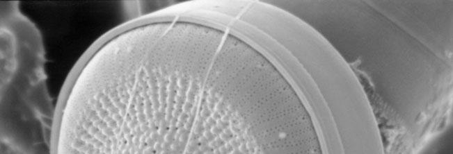
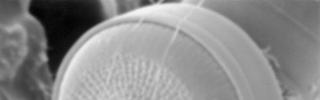
Scanning Electron Microscopy Student Image Portfolio
 SUNY College of Environmental Science and Forestry Digital Commons @ ESF N.C. Brown Center for Ultrastructure Studies Fall 12-7-2016 Scanning Electron Microscopy Student Image Portfolio Matthew DaRin SUNY
Manufacturing Metrology Team
 The Team has a range of state-of-the-art equipment for the measurement of surface texture and form. We are happy to discuss potential measurement issues and collaborative research Manufacturing Metrology
General information. If you see the instrument turned off, notify MIC personnel. MIC personnel will help you insert your samples into the instrument.
 JEOL JSM-7400F Table of contents General information.. 3 The operation panel. 4 The different sample holders and inserting the samples.. 5 Turning on the beam... 6 Stage map control... 8 Correcting astigmatism...
JSM 6060 LV SCANNING ELECTRON MICROSCOPE STANDARD OPERATING PROCEDURES
 JSM 6060 LV SCANNING ELECTRON MICROSCOPE STANDARD OPERATING PROCEDURES RULES All users must go through a series of standard operation procedure training. For more information contact: Longlong Liao Teaching
Schematic diagram of the DAP
 Outline Introduction Transmission mode measurement results Previous emission measurement Trapping mechanics Emission measurement with new circuits Emission images Future plan and conclusion Schematic diagram
Operation Guide. Hitachi S-3400N. Variable Pressure Scanning Electron Microscope. with. Deben Peltier Coolstage
 Operation Guide Hitachi S-3400N Variable Pressure Scanning Electron Microscope with Deben Peltier Coolstage www.deben.co.uk www.taltos.stanford.edu www.hitachi-hta.com Index Main Unit 3 Electron Optical
Scanning Electron Microscope FEI INSPECT F50. Step by step operation manual
 Scanning Electron Microscope FEI INSPECT F50 Step by step operation manual Scanning Electron Microscope, FEI Inspect F50 FE-SEM-F Observation Flow Saving Data And Analysis Specimen preparation Error check
The microscope is useful in making observations and collecting data in scientific experiments. Microscopy involves three basic concepts:
 AP BIOLOGY Chapter 6 NAME DATE Block MICROSCOPE LAB PART I: COMPOUND MICROSCOPE OBJECTIVES: After completing this exercise you should be able to: Demonstrate proper care and use of a compound microscope.
Operating the Hitachi 7100 Transmission Electron Microscope Electron Microscopy Core, University of Utah
 Operating the Hitachi 7100 Transmission Electron Microscope Electron Microscopy Core, University of Utah Follow the procedures below when you use the Hitachi 7100 TEM. Starting Session 1. Turn on the cold
Development of JEM-2800 High Throughput Electron Microscope
 Development of JEM-2800 High Throughput Electron Microscope Mitsuhide Matsushita, Shuji Kawai, Takeshi Iwama, Katsuhiro Tanaka, Toshiko Kuba and Noriaki Endo EM Business Unit, JEOL Ltd. Electron Optics
ELECTRON MICROSCOPY. 09:10 12:00, Oct. 27, 2006 Institute of Physics, Academia Sinica. Tung Hsu
 ELECTRON MICROSCOPY 09:10 12:00, Oct. 27, 2006 Institute of Physics, Academia Sinica Tung Hsu Department of Materials Science and Engineering National Tsinghua University Hsinchu 300, TAIWAN Tel. 03-5742564
SEM Training Notebook
 SEM Training Notebook Lab Manager: Dr. Perry Cheung MSE Fee-For-Service Facility Materials Science and Engineering University of California, Riverside December 21, 2017 (rev. 3.4) 1 Before you begin Complete
Unit Two Part II MICROSCOPY
 Unit Two Part II MICROSCOPY AVERETT 1 0 /9/2013 1 MICROSCOPES Microscopes are devices that produce magnified images of structures that are too small to see with the unaided eye Humans cannot see objects
University of Washington Molecular Analysis Facility
 University of Washington Molecular Analysis Facility Apreo-S (Variable Pressure) is a Schottky Field Emission Scanning Electron Microscope (FESEM) that combines high- and low-voltage ultra-high resolution
Effect of Shot Noise and Secondary Emission Noise in Scanning Electron Microscope Images
 SCANNING VOL. 26, 36 40 (2004) Received: March 7, 2003 FAMS, Inc. Accepted with revision: October 14, 2003 Effect of Shot Noise and Secondary Emission Noise in Scanning Electron Microscope Images K. S.
1.1. In regular TEM imaging mode, find a region of interest and set it at eucentric height.
 JEOL 2010F operating procedure Covers operation in STEM mode (See separate procedures for operation in TEM mode and operation of EDS system) Nicholas G. Rudawski ngr@ufl.edu (805) 252-4916 NOTE: this operating
IMAGE SENSOR SOLUTIONS. KAC-96-1/5" Lens Kit. KODAK KAC-96-1/5" Lens Kit. for use with the KODAK CMOS Image Sensors. November 2004 Revision 2
 KODAK for use with the KODAK CMOS Image Sensors November 2004 Revision 2 1.1 Introduction Choosing the right lens is a critical aspect of designing an imaging system. Typically the trade off between image
Electron Beam Lithography. Adam Ramm
 Electron Beam Lithography Adam Ramm Why use electrons? Negligible diffraction limitations: R = k λ NA With current optical technology, this equates to about 45nm resolution. For an electron, wavelength
Low-energy Electron Diffractive Imaging for Three dimensional Light-element Materials
 Low-energy Electron Diffractive Imaging for Three dimensional Light-element Materials Hitachi Review Vol. 61 (2012), No. 6 269 Osamu Kamimura, Ph. D. Takashi Dobashi OVERVIEW: Hitachi has been developing
PERFORMANCE IN NANOSPACE PRODUCT OVERVIEW
 PERFORMANCE IN NANOSPACE PRODUCT OVERVIEW TESCAN Brno, s.r.o. was established as subsidiary of a multi-national company TESCAN ORSAY HOLDING after the merger (August 2013) of Czech company TESCAN, a global
Tecnai on-line help manual --
 Tecnai on-line help Alignments 1 Tecnai on-line help manual -- Alignments Table of Contents 1 Alignments in the Tecnai microscope...5 2 Alignment procedures...6 3 Introduction to electron optics...11 3.1
A Parallel Radial Mirror Energy Analyzer Attachment for the Scanning Electron Microscope
 142 doi:10.1017/s1431927615013288 Microscopy Society of America 2015 A Parallel Radial Mirror Energy Analyzer Attachment for the Scanning Electron Microscope Kang Hao Cheong, Weiding Han, Anjam Khursheed
A NEW TECHNIQUE TO RAPIDLY IDENTIFY LOW LEVEL GATE OXIDE LEAKAGE IN FIELD EFFECT SEMICONDUCTORS USING A SCANNING ELECTRON MICROSCOPE.
 A NEW TECHNIQUE TO RAPIDLY IDENTIFY LOW LEVEL GATE OXIDE LEAKAGE IN FIELD EFFECT SEMICONDUCTORS USING A SCANNING ELECTRON MICROSCOPE. Jim Colvin Waferscale Integration Inc. 47280 Kato Rd. Fremont, CA 94538
PERFORMANCE IN NANOSPACE PRODUCT OVERVIEW
 PERFORMANCE IN NANOSPACE PRODUCT OVERVIEW TESCAN, a.s. is a Czech joint-stock company focused on research, development and manufacture of scientific instruments and laboratory equipment such as: scanning
Introduction to Transmission Electron Microscopy (Physical Sciences)
") Introduction to Transmission Electron Microscopy (Physical Sciences) Centre for Advanced Microscopy Program 9:30 10:45 Lecture 1 Basics of TEM 10:45 11:00 Morning tea 11:00 12:15 Lecture 2 Diffraction
Introduction to Transmission Electron Microscopy (Physical Sciences) Centre for Advanced Microscopy Program 9:30 10:45 Lecture 1 Basics of TEM 10:45 11:00 Morning tea 11:00 12:15 Lecture 2 Diffraction
Nanotechnology and material science Lecture V
 Most widely used nanoscale microscopy. Based on possibility to create bright electron beam with sub-nm spot size. History: Ernst Ruska (1931), Nobel Prize (1986) For visible light λ=400-700nm, for electrons
Magellan XHR SEM. Discover the world of extreme high resolution scanning electron microscopy
 Magellan XHR SEM Discover the world of extreme high resolution scanning electron microscopy Gold particles on carbon test sample imaged at 200 V and a horizontal field width (HFW) of 500 nm. Unprecedented
Biology The Microscope. May 20 1:19 PM. Using a Microscope to Explore the Cell
 Biology 2201 1.2 The Microscope Using a Microscope to Explore the Cell Resolution or Resolving power The ability of the eye, or other instrument, to distinguish between two objects that are close together
This procedure assumes the user is already familiar with basic operation of the SEM and the MiraTC interface.
 Tescan MIRA3 SEM: EDS using EDAX TEAM Nicholas G. Rudawski ngr@ufl.edu Cell: (805) 252-4916 Office: (352) 392-3077 Last updated: 12/04/17 This procedure assumes the user is already familiar with basic
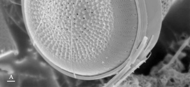
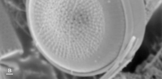
Scanning Electron Microscopy Laboratory Portfolio
 SUNY College of Environmental Science and Forestry Digital Commons @ ESF N.C. Brown Center for Ultrastructure Studies Fall 2016 Scanning Electron Microscopy Laboratory Portfolio Kensey Portman SUNY College
Video. Part I. Equipment
 1 of 7 11/8/2013 11:32 AM There are two parts to this lab that can be done in either order. In Part I you will study the Laws of Reflection and Refraction, measure the index of refraction of glass and
Evaluating the Performance of a Commercial Silicon Drift Detector for X-ray Microanalysis
 Evaluating the Performance of a Commercial Silicon Drift Detector for X-ray Microanalysis Edward A. Kenik Materials Science & Technology Division, Oak Ridge National Laboratory, Oak Ridge, TN 37831 kenikea@ornl.gov
ALTURA EDS. Rev. 0915
 ALTURA EDS Rev. 0915 Enable the Oxford PC Enable the Altura-EDS under Dual Beam Tools in Coral. Or enter your NETID and password directly into the Oxford PC. Warning: Ion-milling, GISs/microprobe, and
Chapter 1. Basic Electron Optics (Lecture 2)
") Chapter 1. Basic Electron Optics (Lecture 2) Basic concepts of microscope (Cont ) Fundamental properties of electrons Electron Scattering Instrumentation Basic conceptions of microscope (Cont ) Ray diagram
Chapter 1. Basic Electron Optics (Lecture 2) Basic concepts of microscope (Cont ) Fundamental properties of electrons Electron Scattering Instrumentation Basic conceptions of microscope (Cont ) Ray diagram
SCANNING ELECTRON MICROSCOPY By W. C. NIXON (Engineering Laboratory, Cambridge University)
") 213 0 Journal of the Royal MicroscopicalSociety, VoZ. 83, Pts. I & 2, June 1964. Pages 213-216 SCANNING ELECTRON MICROSCOPY By W. C. NIXON (Engineering Laboratory, Cambridge University) PLATE 97-98 AND
213 0 Journal of the Royal MicroscopicalSociety, VoZ. 83, Pts. I & 2, June 1964. Pages 213-216 SCANNING ELECTRON MICROSCOPY By W. C. NIXON (Engineering Laboratory, Cambridge University) PLATE 97-98 AND