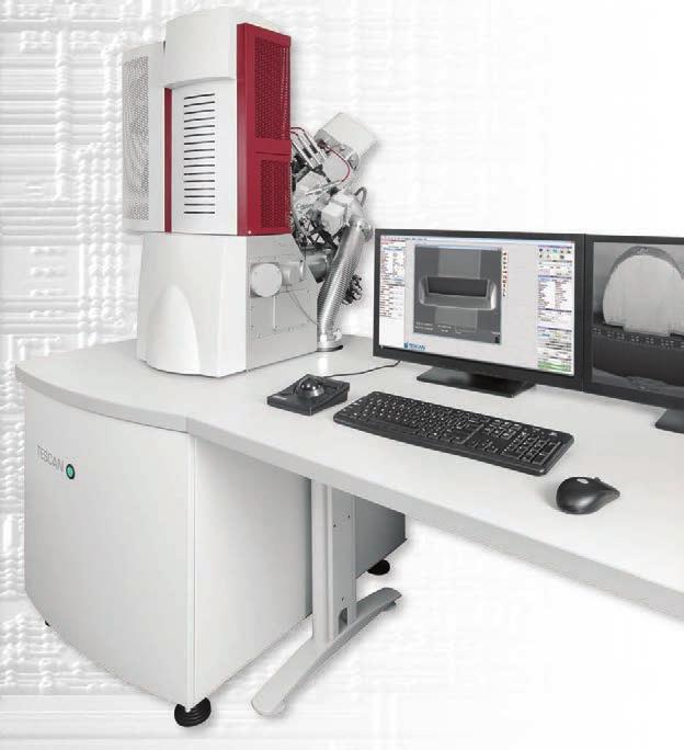
PERFORMANCE IN NANOSPACE PRODUCT OVERVIEW
|
|
|
- Suzan Walker
- 5 years ago
- Views:
Transcription

1 PERFORMANCE IN NANOSPACE PRODUCT OVERVIEW


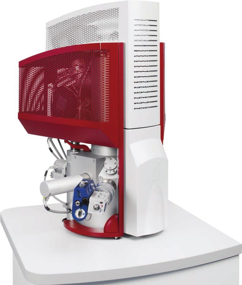
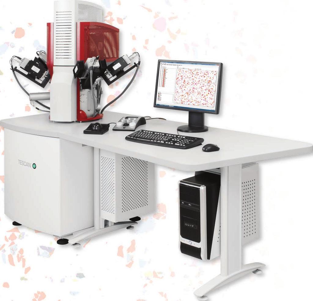
2 TESCAN Brno, s.r.o. was established as subsidiary of a multi-national company TESCAN ORSAY HOLDING after the merger (August 2013) of Czech company TESCAN, a global supplier of SEMs and focused ion beam workstations, and the French company ORSAY PHYSICS, a world leader in customized Focused Ion Beam and Electron Beam technology. TESCAN s product range includes: thermal emission systems LaB6 systems field emission systems FIB and Plasma FIB systems detection systems supplementary accessories for SEMs, FE-SEMs, FIB-SEMs. TESCAN brand (founded in the summer of 1991) is well known for its innovation and openness to work with researchers and customizing applications to fit specific analytical needs. TESCAN excels in development of integrated solutions for scanning electron and focused ion beam microscopy, scientific hardware and software innovations. TESCAN the leading provider of scientific instrumentation continues the tradition of excellence in SEMs. During the 23 years of its existence, the TESCAN brand has built a reputation of quality, reliability and innovation, with over SEMs installed in more than 60 countries. TESCAN PRODUCTS By following progress in electron microscopy and by pioneering and applying new technological possibilities, TESCAN is producing its microscopes to the highest level of technical excellence. By using TESCAN superior tools you will experience the most advanced scanning electron line of instruments. Features of TESCAN Products Modern Optics The development of the entire range of TESCAN systems focuses on the highest standards and competitive advantage for its customers. All TESCAN instruments are equipped with modern optics incorporating advanced technology: A unique Wide Field Optics design with a proprietary Intermediate Lens (IML) in addition to the conventional objective lens offers a variety of working and displaying modes: so called Resolution mode for the highest resolution, Field mode for enhanced field of view, Depth mode for extended depth of focus, Channeling mode for rocking the beam in order to obtain electron channeling patterns and Wide Field mode for extra large field of view. Real time In-Flight Beam Tracing for ultimate performance and beam optimization. Originally developed by TESCAN, this method represents an active way of controlling the electron-optical system. By using a very precise calculation of all optical parameters, it is possible to control the beam current precisely and directly and the spot size continuously for the whole range of the beam energy. TESCAN was first to offer live stereoscopic imaging using advanced 3D Beam Technology which opens up the micro and nano-world for an amazing 3D experience and 3D navigation. 3D Beam Technology allows the scanning axis to tilt around the center of the view field and therefore true live stereo-imaging is possible. The important feature of observation and acquiring of three-dimensional images using TESCAN SEMs is the possibility to generate image series and video sequences by tilting either the beam or stage. Together with 3D reconstruction software, it provides a revolutionary tool for 3D surface analysis. Fast imaging rate without sacrificing image quality. Fully automated electron-optics set-up and alignment. E-Beam lithography available with an optional Beam Blanker. PERFORMANCE IN NANOSPACE


3 Analytical Potential The highest quality and reliability of the TESCAN product range mirrors its strong analytical potential: First-class YAG scintillator-based detectors Selection of optional detectors and accessories Fast and easy attainment of a clean chamber vacuum Investigation of non-conductive samples in variable-pressure mode versions Option of extra-large XM or analytical GM chambers with robust stage able to accommodate large samples (including heavy samples up to 8 kg). LM, XM, GM chamber models provide superior specimen handling using a full 5-axis motorized compucentric stage and ideal geometry for microanalysis. Numerous interface ports with optimized analytical geometry for EDX, WDX and EBSD as well as for attaching many other detectors 3D measurements on a reconstructed surface utilizing 3D metrology software Several chamber suspension options ensure effective reduction of ambient vibrations in the laboratory. Unique integrated active vibration isolation for analytical GM chamber delivered as standard. Automated Procedures Filament heating and alignment of the electron gun for optimal beam performance is achieved automatically with just one click. There are many other automated procedures which reduce the operator s tune-up time significantly, including automated manipulator navigation and automated analyses. SharkSEM remote control interface enables access to most microscope features, including microscope vacuum control, optics control, stage control, image acquisition, etc. The compact Python scripting library offers all these features. User-Friendly Software and Software Tools Multi-user environment is localized in many languages. Easy control of the SEM even for inexperienced users; four levels of user expertise/rights, including an EasySEM mode for quick routine investigations Built-in image management and report creation Built-in self-diagnostics for system readiness checks Network operations and remote control/diagnostics Modular software architecture enables several extensions to be attached. Basic set of plug-ins, such as Measurement, Image Processing, Object Area, available as standard Several optional modules or dedicated applications optimized for automatic sample examination procedures, such as particle analysis or 3D surface reconstruction, etc. Fig. Screenshot showing 3D Tomography module. 5 mm Fig. Image in the Wide Field Mode (forensic tool mark analysis). Fig. TESCAN Color CL detector image of a Fluorite.


4 VEGA3


5 3 rd Generation of VEGA SEMs VEGA is a SEM with conventional tungsten heated cathode intended both for high vacuum as well as for low vacuum operations. After 12 years of continuous development VEGA has matured to its 3 rd generation. The column design without any mechanical centering elements enables fully automated column set-up and alignment. The creation of favorable conditions for complex analysis of specimens, combined with high performance imaging capabilities, were a high priority in the design of the VEGA microscopes from the beginning. The conical objective lens, carefully considered chamber design, high precision compucentric or eucentric stages, wide choice of detectors and supplementary accessories, all combined to make the VEGA3 SEM a versatile and powerful analytical tool. VEGA3 Modifications High Resolution Imaging with LaB6 Emitter Besides the tungsten heated filament TESCAN offers the LaB6 (lanthanum hexaboride) electron source as an option. The LaB6 provides higher current density at lower cathode temperatures compared to tungsten emitters. It offers greater brightness, a reasonably improved resolution over the whole range of accelerating voltages and a longer cathode lifetime. Due to the higher current and smaller spot size, the LaB6 emitter is the right choice for applications where large beam currents and improved resolution are required. VEGA3 Chamber type SB LM Specimen height max. 36 mm max. 81 mm VEGA3 SB EasyProbe Small Chamber, Motorized Stage, Integrated EDX, High Vacuum Operation The VEGA3 SB EasyProbe is a compact scanning electron microscope fully integrated with a selected energy dispersive X-ray microanalyser. Superior imaging quality, high level of automation, easy usage and quick quantitative elemental results directly in the live image are characteristic features of the instrument. Chamber type Specimen height XM max. 145 mm GM max. 145 mm Electron gun Tungsten heated cathode / optionally LaB6 * * LaB6 not available for VEGA3 SB Resolution In high vacuum mode (SE) In low vacuum mode (BSE) Acceleration voltage 3.0 nm at 30 kv / 2.0 nm at 30 kv (LaB6) 3.5 nm at 30 kv / 2.5 nm at 30 kv (LaB6) 200 V to 30 kv Probe current 1 pa to 2 µa

6 MIRA3


.")
7 3 rd Generation of MIRA FE-SEMs The new generation of MIRA field emission scanning electron microscopes is based on a high resolution Schottky field emission emitter. MIRA3 provides users with the advantages of the latest technology, such as, new improved high-performance electronics for faster image acquisition, an ultra-fast scanning system with compensation for static and dynamic image aberrations or scripting for user-defined applications, while at the same time maintaining the best price to performance ratio. Its excellent resolution at high beam currents has proved to be advantageous for analytical applications such as EBSD and WDX. Since MIRA3 model 2012 was launched there is the possibility to set up the optional configuration including the Beam Deceleration Technology for the entire range of TESCAN field emission gun SEMs (MIRA3, LYRA3, FERA3). Beam Deceleration Technology (BDT) Maintaining the primary beam at low energy allows a microscope user to determine very fine surface details which would not be observable at higher beam energies. However, better electron-optical performance of a SEM is achieved at high accelerating voltage. BDT combines both factors, as it is obvious that the best results can be achieved if the primary beam is accelerated to high energy in the electron column and decelerated to low energy shortly before it interacts with the sample. BDT launched by TESCAN consists of a Beam Deceleration Mode (BDM) and a state-of-the-art In-Beam detector designed to detect both the high-angle Back Scattered Electrons under the standard operating conditions and the Secondary Electrons signal in the BDM Beam Deceleration Technology significantly improves resolution at low accelerating voltage and the detected signal is outstanding. It can be also used for achieving very low landing energies down to 50 ev. MIRA3 Chamber type LM XM GM Specimen height max. 81 mm max. 145 mm max. 145 mm Electron gun Resolution In high vacuum mode (SE) In low vacuum mode (BSE) In high vacuum BDM (Beam Deceleration Mode) High brightness Schottky emitter 1.2 nm at 30 kv 2 nm at 30 kv 1.8 at 1 kv Decontaminator The Decontaminator is highly recommended for even better improvement in image quality. In order to remove carbon and organics from the chamber TESCAN offers the decontaminator device as an option. Advantages of Using a Decontaminator The reaction of ubiquitous volatile hydrocarbon molecules in the SEM chamber with the electron beam during scanning results the creation of a dark contamination layer on the specimen surface during sample observation and devalues the investigation. This is even more significant when using a low energy electron beam which has a higher reactivity with carbon containing molecules. Acceleration / landing voltage Probe current 200 V to 30 kv / 50 V to 30 kv with BDT (Beam Deceleration Technology) option 2 pa to 200 na


8 Tescan - produktový katalog 2014_Sestava :26 Stránka 8 MAIA3


9 MAIA3 Charging of non-conductive materials, observation of very thin layers, damaging of sensitive samples these are the problems which many scientists are faced with using scanning electron microscopy e.g. in biology, bioengineering, nanosensor or semiconductor research. The analytical scanning electron microscope MAIA3 is the perfect choice for such applications. MAIA3 demonstrates ultra-high resolution of 1 nm at 15 kv. The resolution performance at 1 kv is 1.4 nm using secondary electrons and 0.8 nm at 30 kv in STEM mode. MAIA3 provides user with ultra-high resolution without compromise The ultra-high resolution scanning electron microscope MAIA3 is based on TESCAN s proven three-lens column equipped with a Schottky field emission gun and the unique construction of TESCAN s 60 degree immersion objective lens. Concerning a wide range of specimens, including non-conductive materials, which set the requirement to keep the primary beam at low energy, the analytical performance of MAIA3 might be further enhanced by Beam Deceleration Technology (BDT) utilization. The BDT option enables the ultra-low electron landing energy imaging with automation down to 50 ev and thus the precise determination of very fine surface details without charging effect or possible damage of the sample. It is highly recommended to combine the BDT with decontaminator. Chamber type Specimen height Electron gun Resolution In high vacuum mode (In-Beam SE) In low vacuum mode (BSE) In high vacuum BDM (Beam Deceleration Mode) Acceleration / landing voltage Probe current MAIA3 LM max. 71 mm XM max. 135 mm GM High brightness Schottky emitter 1.0 nm at 15 kv 2 nm at 30 kv 1.4 nm at 1 kv max. 135 mm 200 V to 30 kv / down to 50 V with BDT (Beam Deceleration Technology) option 2 pa to 200 na Analytical features of MAIA3 The specimen observed in MAIA3 is totally immersed in the strong magnetic field induced by the 60 degree immersion objective lens, which extends into the specimen chamber. The objective lens is narrower than a conventional non-immersion objective, dramatically decreases optical aberrations and provides even more space around samples. Like other TESCAN series, the MAIA3 optics is equipped with the customer proven intermediate lens which makes a wide range of imaging modes possible, e.g. FIELD provides large field of view while the sample remains free of any magnetic field. The detection system consists of TESCAN s proprietary detectors, In-Beam SE, In-Beam BSE as well as SE in Beam Deceleration Mode, all of which are placed inside the column to provide a variety of signals in addition to the standard SE, BSE or STEM detectors placed in the specimen chamber.

10 TIMA

 or VEGA thermal emission scanning electron microscope (TIMA3).")
11 TIMA3 / TIMA3 FEG The TESCAN Integrated Mineral Analyzer (TIMA*) is a SEM-based automated mineralogy solution for the mining and minerals processing industries. TIMA measures mineral abundance, size by size liberation, mineral association and grain size automatically on multiple samples of grain mounts, thin sections or polished sections. Applications include ore characterization, process optimization, remediation and the search for precious metals and rare earths. The TESCAN TIMA is based either on MIRA Schottky field emission (TIMA3 FEG) or VEGA thermal emission scanning electron microscope (TIMA3). Special VEGA column design with permanent gun high-vacuum and the isolation valve significantly increases emission stability and tungsten filament lifetime. The system is available in high-vacuum version as the standard, low-vacuum version as an option. TESCAN s unique technology is based on a completely integrated EDX system which performs full spectrum acquisition at very fast scan speeds. The level of hardware integration of SEM and EDX allows unprecedented acquisition speeds for fully automated data collection, resulting in fast, accurate and reliable results. TIMA software is developed for BSE and EDX data acquisition, processing and analysis. It provides three measurement modules Modal Analysis module, Liberation Analysis module and Bright Phase Search module, each of which is designed to be used for specific task. The Modal Analysis module provides information about mass fractions of minerals in a sample. Liberation analysis module gives information about texture of individual particles. The Bright Phase Search module provides information about associations among minerals of interest and other minerals. TIMA software offers two types of Bright Phase Search analysis basic and advanced with phase filtering. The Classification Builder, a special tool for efficient and understandable classification of minerals, is also integrated into TIMA software. Its important part is a library of minerals, which consists of more than hundred of mineral definitions. Electron gun Resolution In high vacuum mode (SE) In low vacuum mode (BSE) Acceleration voltage TIMA3 / TIMA3 FEG TIMA3 Tungsten heated cathode with extraordinary emission stability and filament lifetime (typically 2500 hours) 3.0 nm at 30 kv 3.5 nm at 30 kv Probe current 1 pa to 2 µa Detectors EDX Detectors Accessories Detectors and Accessories 200 V to 30 kv TIMA3 FEG High brightness Schottky emitter 1.2 nm at 30 kv 2 nm at 30 kv 2 pa to 200 na BSE premium YAG scintillator BSE detector (manual or motorized retractable); SE Everhart-Thornley 4 Silicon Drift Detector (SDD), Peltier cooled (no liquid nitrogen required) Probe current measurement; Touch alarm; IR chamber view camera TIMA Advantages Very fast and fully automated data acquisition process enabled via SEM and EDX high level hardware integration System based on MIRA FE-SEM or VEGA SEM platform proven by customers in many countries Special VEGA column design significantly extending tungsten filament lifetime Exchangeable sample holder with integrated fixed BSE/EDX calibration standard and Faraday cup Possibility to modify size of samples according to customer demands Up to 4 integrated EDX detectors for maximum system performance Peltier cooled EDX detector type for thermal stability guarantee Improved approach to data analysis increasing the speed and reliability of the process Variable dwell time and EDX analysis duration adapting to each part of the sample Software released in three editions Various modules for data analysis Customizable classification rules Favourable price performance ratio Customised solution possibilities * TIMA is available with LM and GM chambers.

12 LYRA3
 scanning electron microscope with the ability to perform surface")

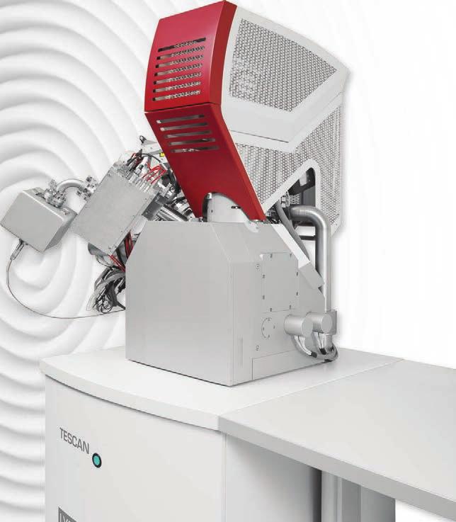
13 LYRA3 The LYRA3 FIB-SEM brings a combination of the electron and high performance ion columns. Built on the MIRA3 platform, LYRA3 extends the imaging qualities of a field emission (high resolution Schottky FEG-SEM Column) scanning electron microscope with the ability to perform surface modification by utilizing a focused ion beam. The LYRA3 series was designed with respect to a wide range of FIB-SEM applications and needs in today s research and industry. Its excellent resolution at high beam currents has proved to be advantageous for analytical applications such as EDX, WDX, EBSD, 3D tomography. The powerful software turns these TESCAN FIB-SEMs into excellent tools for a variety of other applications, such as electron/ion lithography or TEM sample preparation. LYRA3 focused ion beam scanning electron microscope is manufactured in configurations with XM and GM chambers. High Performance Ion Optics The series of focused ion beam scanning electron microscopes LYRA3 are manufactured to incorporate High Performance in Ion Optics. There are two versions of FIB column available: Sophisticated high performance CANION FIB system for fast and precise cross-sectioning and TEM sample preparation Optional ultra-high resolution COBRA-FIB column represents the highest level of technology in terms of resolution both for imaging and milling. This is one of the most precise FIB instruments for nano-engineering in the world. Chamber type Specimen height LYRA3 Electron optics Electron gun Resolution In high vacuum mode (SE) In low vacuum mode (BSE) LYRA3 XM maximum 139 mm GM maximum 139 mm High brightness Schottky emitter 1.2 nm at 30 kv 2 nm at 30 kv Every TESCAN FIB-SEM user takes advantage of following FIB characteristics: Unique ion optic column, differentially pumped, with 2 ion pumps, for ultra-low ion scattering effect Motorized aperture changer with ultra-high reproducibility Beam Blanker and Faraday cup included as a standard Simultaneous SEM imaging with FIB etching or deposition FIB control is fully integrated in the SEM software Powerful and user friendly toolbox for delineation of both basic and complex shape creation with programmable process parameters Micro/nano machining Ion beam lithography Acceleration voltage Probe current 200 V to 30 kv / 50 V to 30 kv with BDT (Beam Deceleration Technology) option 2 pa to 200 na Ion optics Ion column Resolution Accelerating Voltage Ion Gun Probe Current SEM-FIB Coincidence at Canion / Cobra <5 nm at 30 kv / <2.5 nm at 30 kv (at SEM-FIB coincidence point) 0.5 kv to 30 kv Ga Liquid Metal Ion Source 1 pa to 40 na / 1 pa to 50 na WD 9 mm for SEM, WD 12 mm for FIB
14 FERA3


15 FERA3 The world s first fully integrated Xenon Plasma source FIB with SEM enables extremely high ion currents of up to 2 µa thus increasing material sputtering rate. Compared to existing FIB technologies with gallium sources, the material removal rate achievable for silicon with the Plasma FIB-SEM is about 50 times faster. For this reason the FERA3 is well suited for applications requiring the removal of large volumes of material, particularly in the semiconductor packaging environment where TSV technology is being utilized. The unique combination of Xenon plasma source and electron emitter integrates the advantages of high resolution of the SEM with FIB potential into one single device. Therefore, FERA3 allows the user to easily employ the direct observation techniques of the prepared sample; importantly, the positioning of milling without any additional damage to the sample is possible. Generally, systems of this kind can not only be used in materials science, research, forensic investigations but mainly in semiconductor industry for example for 3D metrology, defect and failure analysis or designing of MEMS and TSVs. FERA3 Chamber type XM GM Specimen height maximum 139 mm maximum 139 mm Electron optics Electron gun Resolution In high vacuum mode (SE) In low vacuum mode (BSE) Acceleration / landing voltage Probe current Ion optics Ion column Resolution Accelerating Voltage Ion Gun High brightness Schottky emitter 1.2 nm at 30 kv 2 nm at 30 kv 200 V to 30 kv / 50 V to 30 kv with BDT (Beam Deceleration Technology) option 2 pa to 200 na i-fib 25 nm at 30kV at SEM-FIB coincidence point 3 kv to 30 kv Xe Plasma Ion Source Probe Current 20 pa to 2 µa FERA3 Plasma FIB-SEM configurations Sophisticated high performance Plasma FIB-SEM system for both extremely fast and precise cross sectioning and high volume material removal. FERA3 Plasma FIB-SEM can be configured with gas injection systems, nanomanipulators, and a wide variety of detectors including, for example, SE (Secondary Electron) detector, BSE (Backscattered Electron) detector, SI (Secondary Ion) detector, CL (Cathodoluminescence) detector, EDX and EBSD microanalyzers. SEM-FIB Coincidence at WD 9 mm for SEM WD 12 mm for FIB

 x 315 mm (depth) Door 120 mm (width) 148")
 x 320 mm (height) Number of ports 10 11 + 12")
")


16 CHAMBER TYPES SB LM XM GM TESCAN chamber types overview Chamber type SB LM XM GM Internal dimensions Ø 160 mm Ø 230 mm 285 mm (width) x 340 mm (depth) 340 mm (width) x 315 mm (depth) Door 120 mm (width) 148 mm (width) 285 mm (width) x 320 mm (height) 340 mm (width) x 320 mm (height) Number of ports Chamber suspension mechanical pneumatic pneumatic Active vibration isolation (integrated) Speciment stage semi-motorized fully motorized fully motorized fully motorized Type eucentric compucentric compucentric compucentric Movements X = 45 mm - mot. Y = 45 mm - mot. Z= 27 mm Z'= 6 mm Rotation: 360 mot. X= 80 mm Y= 60 mm Z= 47 mm Rotation: 360 cont. X= 130 mm Y= 130 mm Z= 100 mm Rotation: 360 cont. X = 130 mm Y = 130 mm Z = 100 mm Rotation: 360 cont. PERFORMANCE IN NANOSPACE TESCAN BRNO, s.r.o. Libušina třída 21, Brno, Czech Republic, EU tel , fax , info@tescan.cz TESCAN
PERFORMANCE IN NANOSPACE PRODUCT OVERVIEW
 PERFORMANCE IN NANOSPACE PRODUCT OVERVIEW TESCAN, a.s. is a Czech joint-stock company focused on research, development and manufacture of scientific instruments and laboratory equipment such as: scanning
Modern Optics. Analytical Potential. 3 rd Generation of MIRA FE SEMs. High brightness Schottky emitter for high-resolution/highcurrent/
 Modern Optics High brightness Schottky emitter for high-resolution/highcurrent/ low-noise imaging Unique three-lens Wide Field Optics TM design offering a variety of working and displaying modes Proprietary
Introduction of New Products
 Field Emission Electron Microscope JEM-3100F For evaluation of materials in the fields of nanoscience and nanomaterials science, TEM is required to provide resolution and analytical capabilities that can
MIRA FE-SEMs. 3 rd Generation of
 MIRA3 3 rd Generation of MIRA FE-SEMs The new generation of MIRA field emission scanning electron microscopes (SEMs) provides users with the advantages of the latest technology, such as new improved high-performance
and in PERFORMANCE IN NANOSPACE
 and in PERFORMANCE IN NANOSPACE PERFORMANCE IN NANOSPACE Tescan, s.r.o. is a Czech private company focused on research, development and manufacturing of scientific instruments and laboratory equipment
Scanning electron microscope
 Scanning electron microscope 5 th CEMM workshop Maja Koblar, Sc. Eng. Physics Outline The basic principle? What is an electron? Parts of the SEM Electron gun Electromagnetic lenses Apertures Detectors
University of Washington Molecular Analysis Facility
 University of Washington Molecular Analysis Facility Apreo-S (Variable Pressure) is a Schottky Field Emission Scanning Electron Microscope (FESEM) that combines high- and low-voltage ultra-high resolution
Scanning electron microscope
 Scanning electron microscope 6 th CEMM workshop Maja Koblar, Sc. Eng. Physics Outline The basic principle? What is an electron? Parts of the SEM Electron gun Electromagnetic lenses Apertures Chamber and
Low Voltage Electron Microscope
 LVEM5 Low Voltage Electron Microscope Nanoscale from your benchtop LVEM5 Delong America DELONG INSTRUMENTS COMPACT BUT POWERFUL The LVEM5 is designed to excel across a broad range of applications in material
SCANNING ELECTRON MICROSCOPY AND X-RAY MICROANALYSIS
 SCANNING ELECTRON MICROSCOPY AND X-RAY MICROANALYSIS Robert Edward Lee Electron Microscopy Center Department of Anatomy and Neurobiology Colorado State University P T R Prentice Hall, Englewood Cliffs,
Schottky Emission VP FE-SEM
 Schottky Emission VP FE-SEM Variable Pressure The Scanning Electron Microscope (SEM) has played an important role for many years for research and development of advanced materials in the leading edge of
JEM-F200. Multi-purpose Electron Microscope. Scientific / Metrology Instruments Multi-purpose Electron Microscope
 Scientific / Metrology Instruments Multi-purpose Electron Microscope JEM-F200 Multi-purpose Electron Microscope JEM-F200/F2 is a multi-purpose electron microscope of the new generation to meet today's
Low Voltage Electron Microscope
 LVEM 25 Low Voltage Electron Microscope fast compact powerful Delong America FAST, COMPACT AND POWERFUL The LVEM 25 offers a high-contrast, high-throughput, and compact solution with nanometer resolutions.
LVEM 25. Low Voltage Electron Mictoscope. fast compact powerful
 LVEM 25 Low Voltage Electron Mictoscope fast compact powerful FAST, COMPACT AND POWERFUL The LVEM 25 offers a high-contrast, high-throughput, and compact solution with nanometer resolutions. All the benefits
Magellan XHR SEM. Discover the world of extreme high resolution scanning electron microscopy
 Magellan XHR SEM Discover the world of extreme high resolution scanning electron microscopy Gold particles on carbon test sample imaged at 200 V and a horizontal field width (HFW) of 500 nm. Unprecedented
SCIENTIFIC INSTRUMENT NEWS. Introduction. Design of the FlexSEM 1000
 SCIENTIFIC INSTRUMENT NEWS 2017 Vol. 9 SEPTEMBER Technical magazine of Electron Microscope and Analytical Instruments. Technical Explanation The FlexSEM 1000: A Scanning Electron Microscope Specializing
Scanning Electron Microscopy Basics and Applications
 Scanning Electron Microscopy Basics and Applications Dr. Julia Deuschle Stuttgart Center for Electron Microscopy MPI for Solid State Research Room: 1E15, phone: 0711/ 689-1193 email: j.deuschle@fkf.mpg.de
Low Voltage Electron Microscope. Nanoscale from your benchtop LVEM5. Delong America
 LVEM5 Low Voltage Electron Microscope Nanoscale from your benchtop LVEM5 Delong America DELONG INSTRUMENTS COMPACT BUT POWERFUL The LVEM5 is designed to excel across a broad range of applications in material
M4 TORNADO PLUS. Innovation with Integrity. Super Light Element Micro-XRF Spectrometer. Micro-XRF
 M4 TORNADO PLUS Super Light Element Micro-XRF Spectrometer Innovation with Integrity Micro-XRF M4 TORNADO PLUS - A New Era in Micro-XRF M4 TORNADO PLUS is the world's first Micro-XRF spectrometer that
LVEM 25. Low Voltage Electron Microscope Fast Compact Powerful.... your way to electron microscopy
 LVEM 25 Low Voltage Electron Microscope Fast Compact Powerful... your way to electron microscopy INTRODUCING THE LVEM 25 High Contrast & High Resolution Unmatched contrast of biologic and light material
Leading in Desktop SEM Imaging and Analysis
 Leading in Desktop SEM Imaging and Analysis Fast. Outstanding. Reliable SEM imaging and analysis. The Phenom: World s Fastest Scanning Electron Microscope With its market-leading Phenom desktop Scanning
Transmission Electron Microscopy 9. The Instrument. Outline
 Transmission Electron Microscopy 9. The Instrument EMA 6518 Spring 2009 02/25/09 Outline The Illumination System The Objective Lens and Stage Forming Diffraction Patterns and Images Alignment and Stigmation
Quick and simple installation and no maintenance needed. 3 Times More affordable Than a normal SEM. Obtaining results in less than 4 minutes
 INTRODUCTION We believe that every laboratory working in the field of nanotechnology needs an SEM, therefore we would like to introduce to you our IEM series of SEM. In short space of time, our device
2014 HTD-E with options
 with options The HT7700 : a user-friendly, ergonomic digital TEM with options User-Friendly r end Design Ambient light operation. Multiple automated functions for alignment, focus and stigmation as standard
Scanning Electron Microscope. Instructions for Use
 Scanning Electron Microscope Instructions for Use The reproduction, transmission or use of this document or its contents is not permitted without express written authority. Offenders are liable for damages.
MODULE I SCANNING ELECTRON MICROSCOPE (SEM)
") MODULE I SCANNING ELECTRON MICROSCOPE (SEM) Scanning Electron Microscope (SEM) Initially, the plan of SEM was offered by H. Stintzing in 1927 (a German patent application). His suggested procedure was
MODULE I SCANNING ELECTRON MICROSCOPE (SEM) Scanning Electron Microscope (SEM) Initially, the plan of SEM was offered by H. Stintzing in 1927 (a German patent application). His suggested procedure was
INTRODUCTION We believe that every laboratory working in the field of nanotechnology needs an SEM, therefore we would like to introduce to you our IEM
 INTRODUCTION We believe that every laboratory working in the field of nanotechnology needs an SEM, therefore we would like to introduce to you our IEM series of SEM. In short space of time, our device
The Reverberation of Successful Participation in European Cooperation Schemas
 The Reverberation of Successful Participation in European Cooperation Schemas Zora Střelcová Project Manager TESCAN Brno, s.r.o. zora.strelcova@tescan.cz HORIZON 2020 EUROPEAN UNION FUNDING FOR RESEARCH
Full-screen mode Popup controls. Overview of the microscope user interface, TEM User Interface and TIA on the left and EDS on the right
 Quick Guide to Operating FEI Titan Themis G2 200 (S)TEM: TEM mode Susheng Tan Nanoscale Fabrication and Characterization Facility, University of Pittsburgh Office: M104/B01 Benedum Hall, 412-383-5978,
Triple Beam FIB-SEM-Ar(Xe) Combined System NX2000
 Combined System NX2000") SCIENTIFIC INSTRUMENT NEWS 2017 Vol. 8 M A R C H Technical magazine of Electron Microscope and Analytical Instruments. Technical Explanation Triple Beam FIB-SEM-Ar(Xe) Combined System NX2000 Masahiro Kiyohara
SCIENTIFIC INSTRUMENT NEWS 2017 Vol. 8 M A R C H Technical magazine of Electron Microscope and Analytical Instruments. Technical Explanation Triple Beam FIB-SEM-Ar(Xe) Combined System NX2000 Masahiro Kiyohara
Add CLUE to your SEM. High-efficiency CL signal-collection. Designed for your SEM and application. Maintains original SEM functionality
 Add CLUE to your SEM Designed for your SEM and application The CLUE family offers dedicated CL systems for imaging and spectroscopic analysis suitable for most SEMs. In addition, when combined with other
Functions of the SEM subsystems
 Functions of the SEM subsystems Electronic column It consists of an electron gun and two or more electron lenses, which influence the path of electrons traveling down an evacuated tube. The base of the
ZEISS EVO SOP. May 2017 ELECTRON OPTICS
 ZEISS EVO SOP May 2017 ELECTRON OPTICS The patented EVO column is the area of the SEM, where electrons are emitted, accelerated, deflected, focused, and scanned. Main characteristics of the EVO optics
Oct. 30th- Nov. 1st, 2017
 Thomas LaGrange, Ph.D. Faculty Lecturer and Senior Staff Scientist Electron Sources, Optics and Detectors SEM Doctoral Course MS-636 Oct. 30th- Nov. 1st, 2017 Summary Electron propagation is only possible
STEP INTO THE WORLD OF JEOL
 Product Lineup SMART FLEXIBLE POWERFUL STEP INTO THE WORLD OF JEOL SEM TEM SAMPLE PREP NMR MASS SPEC EPMA LITHOGRAPHY Bell Lab Harvard University Osaka University JEOLUSA.COM CRYO-EM, EPMA, LITHOGRAPHY
PRISMAPLUS. The precise solution for mass spectrometry. Modular design. Powerful software. Wide range of applications.
 PRISMAPLUS The precise solution for mass spectrometry. Modular design. Powerful software. Wide range of applications. PRISMAPLUS The precise solution for mass spectrometry. The combination of high sensi
Oct. 30th- Nov. 1st, 2017
 Thomas LaGrange, Ph.D. Faculty Lecturer and Senior Staff Scientist Electron Sources, Optics and Detectors SEM Doctoral Course MS-636 Oct. 30th- Nov. 1st, 2017 Summary Electron propagation is only possible
NANO MODIFICATION OF THE W(100)/ZrO ELECTRON EMITTER TIP USING REACTIVE ION ETCHING
/ZrO ELECTRON EMITTER TIP USING REACTIVE ION ETCHING") NANO MODIFICATION OF THE W(100)/ZrO ELECTRON EMITTER TIP USING REACTIVE ION ETCHING Miroslav HORÁČEK, František MATĚJKA, Vladimír KOLAŘÍK, Milan MATĚJKA, Michal URBÁNEK Ústav přístrojové techniky AV ČR,
NANO MODIFICATION OF THE W(100)/ZrO ELECTRON EMITTER TIP USING REACTIVE ION ETCHING Miroslav HORÁČEK, František MATĚJKA, Vladimír KOLAŘÍK, Milan MATĚJKA, Michal URBÁNEK Ústav přístrojové techniky AV ČR,
Ion Beam Lithography next generation nanofabrication
 Ion Beam Lithography next generation nanofabrication EFUG Bordeaux 2011 ion beams develop Lloyd Peto IBL sales manager Copyright 2011 by Raith GmbH ionline new capabilities You can now Apply an ion beam
2.Components of an electron microscope. a) vacuum systems, b) electron guns, c) electron optics, d) detectors. Marco Cantoni 021/
 vacuum systems, b) electron guns, c) electron optics, d) detectors. Marco Cantoni 021/") 2.Components of an electron microscope a) vacuum systems, b) electron guns, c) electron optics, d) detectors, 021/693.48.16 Centre Interdisciplinaire de Microscopie Electronique CIME Summary Electron propagation
2.Components of an electron microscope a) vacuum systems, b) electron guns, c) electron optics, d) detectors, 021/693.48.16 Centre Interdisciplinaire de Microscopie Electronique CIME Summary Electron propagation
PrismaPlus. The New Mass Spectrometer with the Added Plus! Modular Design. Powerful Software. Wide Range of Applications.
 PrismaPlus The New Mass Spectrometer with the Added Plus! Modular Design. Powerful Software. Wide Range of Applications. PrismaPlus The PrismaPlus innovation The optimum combination of high sensitivity,
ELECTRON MICROSCOPY. 13:10 16:00, Oct. 6, 2008 Institute of Physics, Academia Sinica. Tung Hsu
 ELECTRON MICROSCOPY 13:10 16:00, Oct. 6, 2008 Institute of Physics, Academia Sinica Tung Hsu Department of Materials Science and Engineering National Tsing Hua University Hsinchu 300, TAIWAN Tel. 03-5742564
Introduction: Why electrons?
 Introduction: Why electrons? 1 Radiations Visible light X-rays Electrons Neutrons Advantages Not very damaging Easily focused Eye wonderful detector Small wavelength (Angstroms) Good penetration Small
contents TABLE OF The SECOM platform Applications - sections Applications - whole cells Features Integrated workflow Automated overlay
 S E C O M TABLE OF contents The SECOM platform 4 Applications - sections 5 Applications - whole cells 8 Features 9 Integrated workflow 12 Automated overlay ODEMIS - integrated software Specifications 13
Recent results from the JEOL JEM-3000F FEGTEM in Oxford
 Recent results from the JEOL JEM-3000F FEGTEM in Oxford R.E. Dunin-Borkowski a, J. Sloan b, R.R. Meyer c, A.I. Kirkland c,d and J. L. Hutchison a a b c d Department of Materials, Parks Road, Oxford OX1
Appreciating the very little things: Status and future prospects of TEM at NUANCE
 Appreciating the very little things: Status and future prospects of TEM at NUANCE Dr. Roberto dos Reis roberto.reis@northwestern.edu 11/28/2018 Nature 542, pages75 79 (2017) TEM Facility Manager: Dr. Xiaobing
Introduction to Scanning Electron Microscopy
 Introduction to Scanning Electron Microscopy By: Brandon Cheney Ant s Leg Integrated Circuit Nano-composite This document was created as part of a Senior Project in the Materials Engineering Department
2.Components of an electron microscope. a) vacuum systems, b) electron guns, c) electron optics, d) detectors. Marco Cantoni, 021/
 vacuum systems, b) electron guns, c) electron optics, d) detectors. Marco Cantoni, 021/") 2.Components of an electron microscope a) vacuum systems, b) electron guns, c) electron optics, d) detectors Marco Cantoni, 021/693.48.16 Centre Interdisciplinaire de Microscopie Electronique CIME MSE-603
2.Components of an electron microscope a) vacuum systems, b) electron guns, c) electron optics, d) detectors Marco Cantoni, 021/693.48.16 Centre Interdisciplinaire de Microscopie Electronique CIME MSE-603
PicoMaster 100. Unprecedented finesse in creating 3D micro structures. UV direct laser writer for maskless lithography
 UV direct laser writer for maskless lithography Unprecedented finesse in creating 3D micro structures Highest resolution in the market utilizing a 405 nm diode laser Structures as small as 300 nm 375 nm
Spotlight 150 and 200 FT-IR Microscopy Systems
 S P E C I F I C A T I O N S Spotlight 150 and 200 FT-IR Microscopy Systems FT-IR Microscopy Spotlight 200 with Frontier FT-IR Spectrometer Introduction PerkinElmer Spotlight FT-IR Microscopy Systems are
ICP-MS. plasma 3. Multi-Collector ICP-MS.
 ICP-MS plasma 3 Multi-Collector ICP-MS www.nu-ins.com plasma 3 is a third generation Multi Collector ICP Mass Spectrometer (MC-ICP-MS), designed to provide the best possible precision and accuracy for
Scanning Electron Microscopy SEM. Warren Straszheim, PhD MARL, 23 Town Engineering
 Scanning Electron Microscopy SEM Warren Straszheim, PhD MARL, 23 Town Engineering wesaia@iastate.edu 515-294-8187 How it works Create a focused electron beam Accelerate it Scan it across the sample Map
Scanning Electron Microscopy
 Scanning Electron Microscopy For the semiconductor industry A tutorial Titel Vorname Nachname Titel Jobtitle, Bereich/Abteilung Overview Scanning Electron microscopy Scanning Electron Microscopy (SEM)
Dickinson College Department of Geology
 Dickinson College Department of Geology Title: Equipment: BASIC OPERATION OF THE SCANNING ELECTRON MICROSCOPE (SEM) JEOL JSM-5900 SCANNING ELECTRON MICROSCOPE Revision: 2.2 Effective Date: 1/29/2003 Author(s):
Electron Sources, Optics and Detectors
 Thomas LaGrange, Ph.D. Faculty Lecturer and Senior Staff Scientist Electron Sources, Optics and Detectors TEM Doctoral Course MS-637 April 16 th -18 th, 2018 Summary Electron propagation is only possible
SECONDARY ELECTRON DETECTION
 SECONDARY ELECTRON DETECTION CAMTEC Workshop Presentation Haitian Xu June 14 th 2010 Introduction SEM Raster scan specimen surface with focused high energy e- beam Signal produced by beam interaction with
Fabrication of Probes for High Resolution Optical Microscopy
 Fabrication of Probes for High Resolution Optical Microscopy Physics 564 Applied Optics Professor Andrès La Rosa David Logan May 27, 2010 Abstract Near Field Scanning Optical Microscopy (NSOM) is a technique
This document assumes the user is already familiar with basic operation of the instrument in TEM mode and use of the Microscope Control interface.
 FEI Tecnai F20 S/TEM: imaging in STEM mode Nicholas G. Rudawski ngr@ufl.edu (805) 252-4916 (352) 392-3077 Last updated: 05/10/18 This document assumes the user is already familiar with basic operation
v tome x m microfocus CT
 GE Inspection Technologies v tome x m microfocus CT Uniting premium 3D metrology and inspection with quality and speed. gemeasurement.com/ct x plore precision CT line Inspect with precision, power, and
The user should already be familiar with operation of the instrument in STEM mode, use of the Microscope Control interface, and TIA.
 FEI Tecnai F20 S/TEM: EDS system operation Nicholas G. Rudawski ngr@ufl.edu (805) 252-4916 (352) 392-3077 Last updated: 01/22/18 The user should already be familiar with operation of the instrument in
attocfm I for Surface Quality Inspection NANOSCOPY APPLICATION NOTE M01 RELATED PRODUCTS G
 APPLICATION NOTE M01 attocfm I for Surface Quality Inspection Confocal microscopes work by scanning a tiny light spot on a sample and by measuring the scattered light in the illuminated volume. First,
2. Raise HT to 200kVby following the procedure explained in 1.6.
 JEOL 2100 MANUAL Quick check list 1. If needed, fill the reservoir with LN2 2. Raise HT to 200kVby following the procedure explained in 1.6. 3. Insert specimen holder into TEM (Insert holder in airlock,
PRISMAPRO. The latest generation of compact mass spectrometers. Modular design. Powerful software. Low detection limit.
 The latest generation of compact mass spectrometers. Modular design. Powerful software. Low detection limit. The latest generation of compact mass spectrometers. The combination of high sensi tivity, maximum
Strata DB235 FESEM FIB
 Strata DB235 FESEM FIB Standard Operating Procedure Revision: 5.0 Last Updated: August 16/2016, revised by Li Yang Overview This document will provide a detailed operation procedure of the Focused Ion
Scanning Electron Microscopy. EMSE-515 F. Ernst
 Scanning Electron Microscopy EMSE-515 F. Ernst 1 2 Scanning Electron Microscopy Max Knoll Manfred von Ardenne Manfred von Ardenne Principle of Scanning Electron Microscopy 3 Principle of Scanning Electron
BRUKER ADVANCED X-RAY SOLUTIONS. SPECTROMETRY SOLUTIONS ARTAX mxrf SPECTROMETER
 BRUKER ADVANCED X-RAY SOLUTIONS SPECTROMETRY SOLUTIONS ARTAX mxrf SPECTROMETER Microanalysis ARTAX Elemental Analysis for the Art Community and More Non-destructive elemental analysis is strictly required
Scanning Electron Microscope FEI INSPECT F50. Step by step operation manual
 Scanning Electron Microscope FEI INSPECT F50 Step by step operation manual Scanning Electron Microscope, FEI Inspect F50 FE-SEM-F Observation Flow Saving Data And Analysis Specimen preparation Error check
TRITON Plus Thermal Ionization MS. Another step ahead. in TIMS. Earth and Planetary Sciences Nuclear Sciences
 TRITON Plus Thermal Ionization MS Another step ahead in TIMS Earth and Planetary Sciences Nuclear Sciences Based on more than 35 years of experience in variable multicollector instrumentation, we have
ELECTRON MICROSCOPY AN OVERVIEW
 ELECTRON MICROSCOPY AN OVERVIEW Anjali Priya 1, Abhishek Singh 2, Nikhil Anand Srivastava 3 1,2,3 Department of Electrical & Instrumentation, Sant Longowal Institute of Engg. & Technology, Sangrur, India.
ARTAX. Innovation with Integrity. Portable Micro-XRF Spectrometer. Micro-XRF
 ARTAX Portable Micro-XRF Spectrometer Innovation with Integrity Micro-XRF ARTAX Elemental Analysis for the Art Community and More The ARTAX is the first portable X ray fluorescence (XRF) spectrometer designed
General information. If you see the instrument turned off, notify MIC personnel. MIC personnel will help you insert your samples into the instrument.
 JEOL JSM-7400F Table of contents General information.. 3 The operation panel. 4 The different sample holders and inserting the samples.. 5 Turning on the beam... 6 Stage map control... 8 Correcting astigmatism...
Development of JEM-2800 High Throughput Electron Microscope
 Development of JEM-2800 High Throughput Electron Microscope Mitsuhide Matsushita, Shuji Kawai, Takeshi Iwama, Katsuhiro Tanaka, Toshiko Kuba and Noriaki Endo EM Business Unit, JEOL Ltd. Electron Optics
1.2. Make sure the viewing screen is covered (exposure to liquid N 2 may cause it to crack).
.") FEI Tecnai F20 S/TEM: imaging in TEM mode Nicholas G. Rudawski ngr@ufl.edu (805) 252-4916 (352) 392-3077 Last updated: 01/21/18 1. Filling the cold trap (if needed) 1.1. Prior to use, the cold trap needs
FEI Tecnai F20 S/TEM: imaging in TEM mode Nicholas G. Rudawski ngr@ufl.edu (805) 252-4916 (352) 392-3077 Last updated: 01/21/18 1. Filling the cold trap (if needed) 1.1. Prior to use, the cold trap needs
OPERATION OF THE HITACHI S-450 SCANNING ELECTRON MICROSCOPE. by Doug Bray Department of Biological Sciences University of Lethbridge
 OPERATION OF THE HITACHI S-450 SCANNING ELECTRON MICROSCOPE by Doug Bray Department of Biological Sciences University of Lethbridge Revised September, 2000 Note: The terms in bold in this document represent
5. The Scanning Electron Microscope
 Physical Principles of Electron Microscopy 5. The Scanning Electron Microscope Ray Egerton University of Alberta and National Institute of Nanotechnology Edmonton, Canada www.tem-eels.ca regerton@ualberta.ca
Basic Operating Instructions for Strata Dual Beam 235 FIB/SEM
 Basic Operating Instructions for Strata Dual Beam 235 FIB/SEM Warning Always adjust your specimen height before closing the chamber door to make sure your specimen will not hit the bottom of the lens;
:... resolution is about 1.4 μm, assumed an excitation wavelength of 633 nm and a numerical aperture of 0.65 at 633 nm.
 PAGE 30 & 2008 2007 PRODUCT CATALOG Confocal Microscopy - CFM fundamentals :... Over the years, confocal microscopy has become the method of choice for obtaining clear, three-dimensional optical images
Scanning Electron Microscope in Our Facility
 SEM Training Scanning Electron Microscope in Our Facility Specifications Table SEM ESEM FE-SEM-F FE-SEM-J FE-SEM-H FE-SEM-CZ Device name TM3030 Inspect S50 Inspect F50 JSM-7600 S-4700 Marlin compact Company
Using the Hitachi 3400-N VP-SEM
 Using the Hitachi 3400-N VP-SEM Opening the Chamber to Load Specimens (This may also be done later using the software) 1. Click the AIR button on the front of the machine: 2. Wait a few minutes until you
Topics 3b,c Electron Microscopy
 Topics 3b,c Electron Microscopy 1.0 Introduction and History 1.1 Characteristic Information 2.0 Basic Principles 2.1 Electron-Solid Interactions 2.2 Electromagnetic Lenses 2.3 Breakdown of an Electron
Development of a Small Residual Gas Analyzer Utilizing the Quadrupole Array Structure Micropole System ~ QL Series ~
 F e a t u r e A r t i c l e Feature Article Development of a Small Residual Gas Analyzer Utilizing the Quadrupole Array Structure Micropole System ~ QL Series ~ Hirokazu Kitaura The Micropole System is
Physical Properties Measurement System (PPMS): Detailed specifications: Basic unit cryogen- free
: Detailed specifications: Basic unit cryogen- free") Physical Properties Measurement System (PPMS): A Cryogen-free Physical Properties Measurement system that operates over a wider range of temperature and magnetic fields: fully automated/computer controlled
Physical Properties Measurement System (PPMS): A Cryogen-free Physical Properties Measurement system that operates over a wider range of temperature and magnetic fields: fully automated/computer controlled
Product Information Version 1.1. ZEISS Xradia 410 Versa Submicron X-ray Imaging: Bridge the Gap in Lab-based Microscopy
 Product Information Version 1.1 ZEISS Xradia 410 Versa Submicron X-ray Imaging: Bridge the Gap in Lab-based Microscopy A Workhorse Solution for Your 3D Submicron Imaging Xradia 410 Versa bridges the gap
(Refer Slide Time: 00:10)
") Fundamentals of optical and scanning electron microscopy Dr. S. Sankaran Department of Metallurgical and Materials Engineering Indian Institute of Technology, Madras Module 03 Unit-6 Instrumental details
Fundamentals of optical and scanning electron microscopy Dr. S. Sankaran Department of Metallurgical and Materials Engineering Indian Institute of Technology, Madras Module 03 Unit-6 Instrumental details
Sensors and Metrology - 2 Optical Microscopy and Overlay Measurements
 Sensors and Metrology - 2 Optical Microscopy and Overlay Measurements 1 Optical Metrology Optical Microscopy What is its place in IC production? What are the limitations and the hopes? The issue of Alignment
Micro-manipulated Cryogenic & Vacuum Probe Systems
 Janis micro-manipulated probe stations are designed for non-destructive electrical testing using DC, RF, and fiber-optic probes. They are useful in a variety of fields including semiconductors, MEMS, superconductivity,
Evaluating the Performance of a Commercial Silicon Drift Detector for X-ray Microanalysis
 Evaluating the Performance of a Commercial Silicon Drift Detector for X-ray Microanalysis Edward A. Kenik Materials Science & Technology Division, Oak Ridge National Laboratory, Oak Ridge, TN 37831 kenikea@ornl.gov
attocube systems Probe Stations for Extreme Environments CRYOGENIC PROBE STATION fundamentals principles of cryogenic probe stations
 PAGE 88 & 2008 2007 PRODUCT CATALOG CRYOGENIC PROBE STATION fundamentals...................... 90 principles of cryogenic probe stations attocps I.......................... 92 ultra stable cryogenic probe
Hiding In Plain Sight. How Ultrasonics Can Help You Find the Smallest Bonded Wafer and Device Defects. A Sonix White Paper
 Hiding In Plain Sight How Ultrasonics Can Help You Find the Smallest Bonded Wafer and Device Defects A Sonix White Paper If You Can See It, You Can Solve It: Understanding Ultrasonic Inspection of Bonded
Revolutionizing 2D measurement. Maximizing longevity. Challenging expectations. R2100 Multi-Ray LED Scanner
 Revolutionizing 2D measurement. Maximizing longevity. Challenging expectations. R2100 Multi-Ray LED Scanner A Distance Ahead A Distance Ahead: Your Crucial Edge in the Market The new generation of distancebased
MSE 595T Transmission Electron Microscopy. Laboratory III TEM Imaging - I
 MSE 595T Basic Transmission Electron Microscopy TEM Imaging - I Purpose The purpose of this lab is to: 1. Make fine adjustments to the microscope alignment 2. Obtain a diffraction pattern 3. Obtain an
Scanning Electron MICROSCOPES. SEM-20/30, TableTop SEM-20. The Wise SEM for Your Application
 SEM-20/30, TableTop SEM-20 The Wise SEM for Your Application Navigation to Nanoworld With SEM How do you keep the forefront from competition in researching nanometer small world. MRC provides convenient
Low-energy Electron Diffractive Imaging for Three dimensional Light-element Materials
 Low-energy Electron Diffractive Imaging for Three dimensional Light-element Materials Hitachi Review Vol. 61 (2012), No. 6 269 Osamu Kamimura, Ph. D. Takashi Dobashi OVERVIEW: Hitachi has been developing
FEI Tecnai G 2 F20 Operating Procedures
 FEI Tecnai G 2 F20 Operating Procedures 1. Startup (1) Sign-up in the microscope log-sheet. Please ensure you have written an account number for billing. (2) Log in to the computer: Login to your account
nanovea.com PROFILOMETERS 3D Non Contact Metrology
 PROFILOMETERS 3D Non Contact Metrology nanovea.com PROFILOMETER INTRO Nanovea 3D Non-Contact Profilometers are designed with leading edge optical pens using superior white light axial chromatism. Nano
Instructions for Tecnai a brief start up manual
 Instructions for Tecnai a brief start up manual Version 3.0, 8.12.2015 Manual of Tecnai 12 transmission electron microscope located at Aalto University's Nanomicroscopy Center. More information of Nanomicroscopy
Difrotec Product & Services. Ultra high accuracy interferometry & custom optical solutions
 Difrotec Product & Services Ultra high accuracy interferometry & custom optical solutions Content 1. Overview 2. Interferometer D7 3. Benefits 4. Measurements 5. Specifications 6. Applications 7. Cases
Basic Users Manual for Tecnai-F20 TEM
 Basic Users Manual for Tecnai-F20 TEM NB: This document contains my personal notes on the operating procedure of the Tecnai F20 and may be used as a rough guide for those new to the microscope. It may
Transmissions Electron Microscopy (TEM)
") Transmissions Electron Microscopy (TEM) Basic principles Diffraction Imaging Specimen preparation A.E. Gunnæs MENA3100 V17 TEM is based on three possible set of techniqes Diffraction From regions down
Transmissions Electron Microscopy (TEM) Basic principles Diffraction Imaging Specimen preparation A.E. Gunnæs MENA3100 V17 TEM is based on three possible set of techniqes Diffraction From regions down