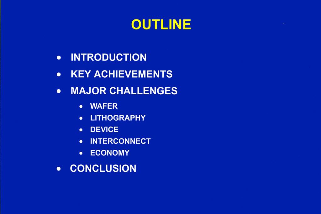
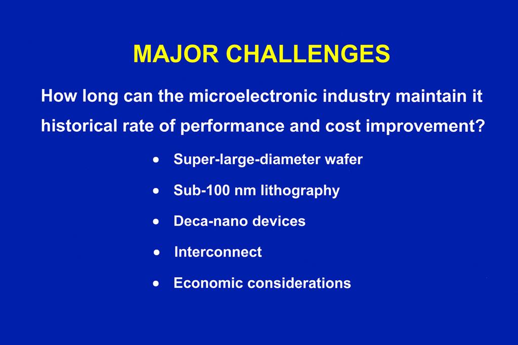
NANOELECTRONIC TECHNOLOGY: CHALLENGES IN THE 21st CENTURY
|
|
|
- Gordon Walton
- 5 years ago
- Views:
Transcription
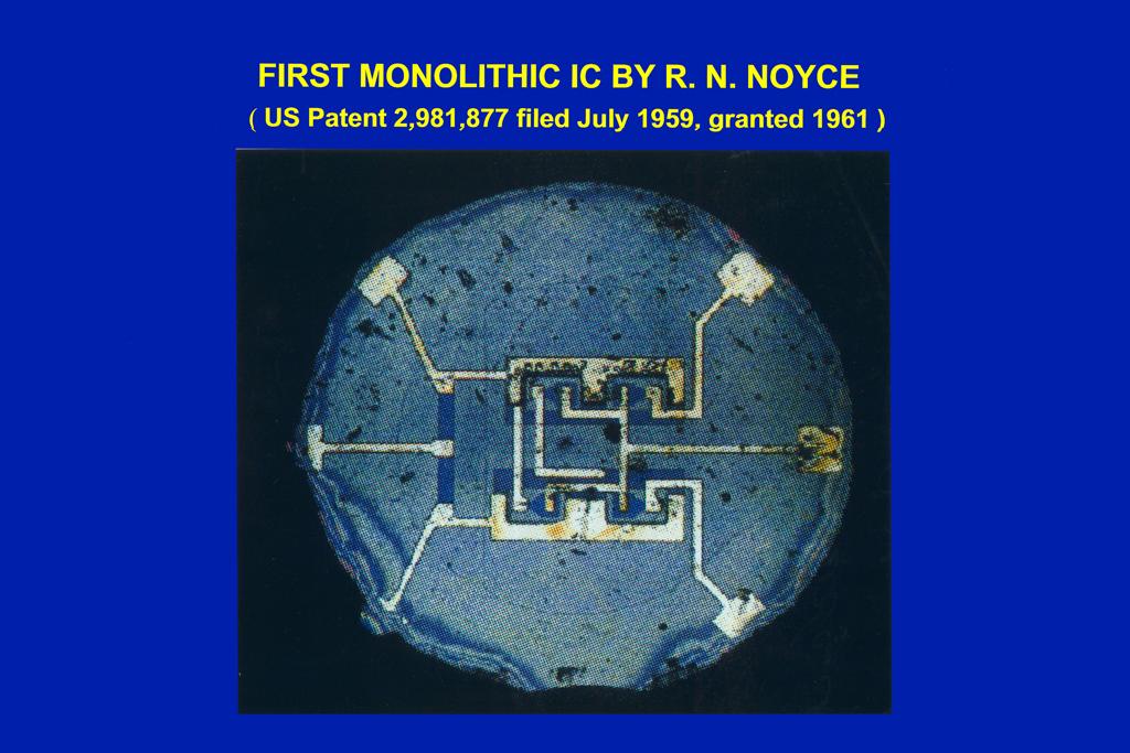
1 NANOELECTRONIC TECHNOLOGY: CHALLENGES IN THE 21st CENTURY S. M. SZE National Chiao Tung University Hsinchu, Taiwan And Stanford University Stanford, California
2
3
4 ELECTRONIC AND SEMICONDUCTOR INDUSTRIES ( ) 10 5 GWP 100 GLOBAL SALES ($Billions) ELECTRONICS AUTOMOBILES SEMICONDUCTOR STEEL SALES ($Trillions) YEAR
5
6
7
8

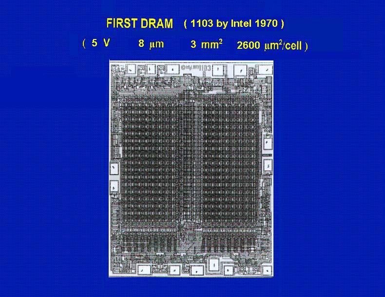
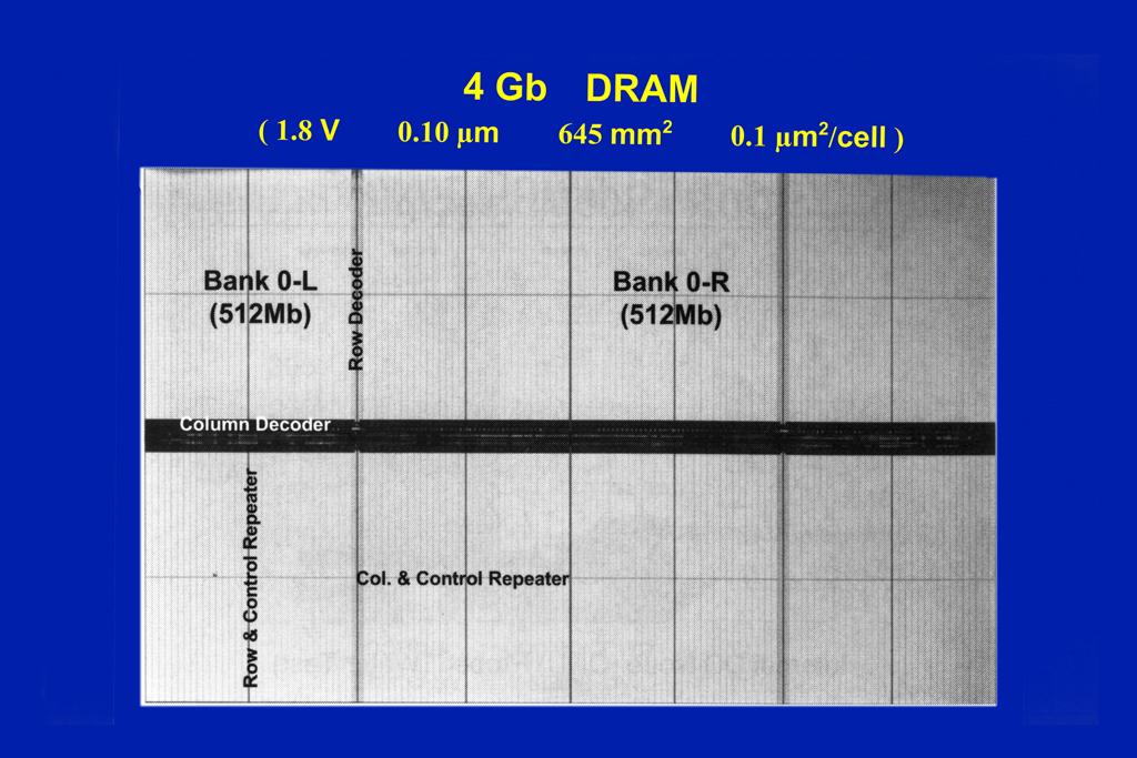
9 32 Gb FLASH MEMORY ( 17 V 40nm 230 mm μm 2 /cell )
10 MOORE S LAW MEMORY DENSITY DRAM 64kb 256kb 1Mb 4Mb 16Mb 64Mb FLASH 256Mb 1Gb 4Gb 128Gb 64Gb 32Gb 16Gb 2Gb FLASH DRAM MOORE'S LAW ( x 4 / 3 YEAR) YEAR
 ( 2300 Transistors 12 mm 2 8μm 750 khz")
11 FIRST MICROPROCESSOR ( 4004 by Intel 1971 ) ( 2300 Transistors 12 mm 2 8μm 750 khz )

12 ITANIUM MICROPROCESSOR ( 1.72 Billion Transistors 90nm 595 mm2 2 GHz )
13 CPU PERFORMANCE TREND ( )
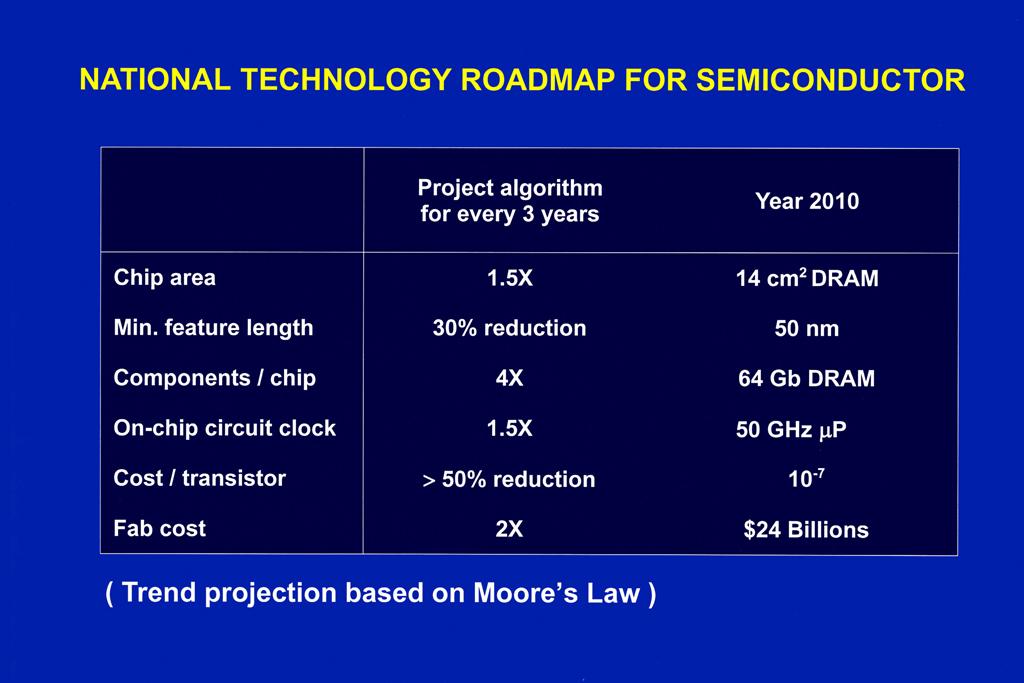
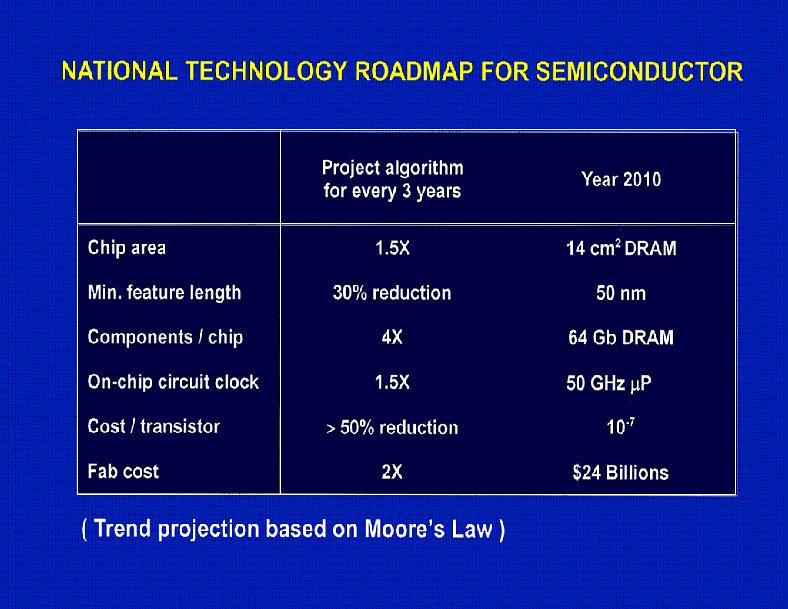
14 PROGRESS IN MICROELECTRONICS Year Ratio Design Rule (μm) V DD (V) Wafer diameter (mm) Devices per chip DRAM density (bit) 1k 2G Nonvolatile memory density (bit) 2k 32G Microprocessor performance (MIPS) Transistor shipped / year Average transistor price ($)
15
16
17
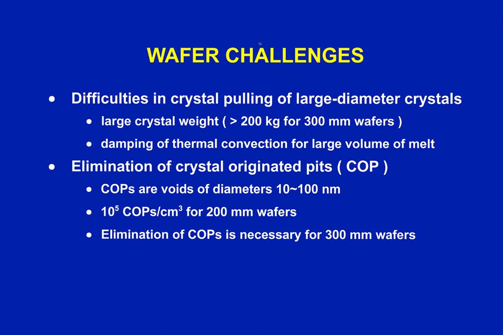
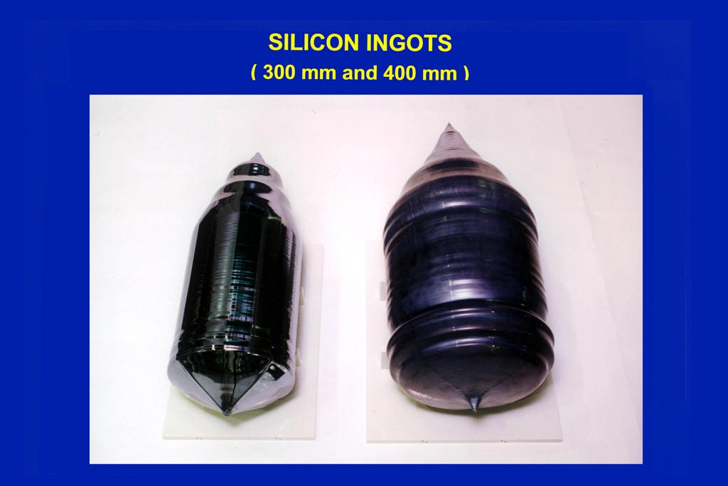
18 450 mm SILICON WAFERS Production Cost For Cu/low K 32 nm process, the production cost per unit wafer area is expected to be reduced by 20~25% as compared to 300 mm wafer Initial Production Intel, Samsung, and TSMC are planning their pilot productions around
19 LITHOGRAPHY CHALLENGES Optical Lithography How far can immersion lens and hologram masks extend the 193 nm ArF system? Do we need the EUV system to support sub-25nm technology nodes? Nonoptical lithography systems Electron-beam projection lithography (EPL) X-Ray lithography (XRL) lon-beam projection lithography (lpl) Lithography-independent nanotechnology Vertical MOSFET Self-assemble Self-organization
20 OPTICAL LITHOGRAPHY OPTIONS Water-Based Immersion with Double Patterning most straight forward extension of 193 nm lithography system, but will double the cost severe impact on tool requirement like overlay Non-Water-Based Immersion use liquid with refractive index higher than water to increase NA ( >1.35 ) require currently unavailable lens materials Extreme-Ultra-Violet (EUV) System with λ =13.5nm EUV is the most extendable lithography technology first full-field tools available in 2006 additional progress needed on EUV sources, resists, and masks
21 DEVICE CHALLENGES Planar MOSFET Scaling MOSFET with Performance Boosters Quasi-planar SOI FinFET Logic Device Options Nonvolatile Semiconductor Memory (NVSM) Nonvolatile Memory Options
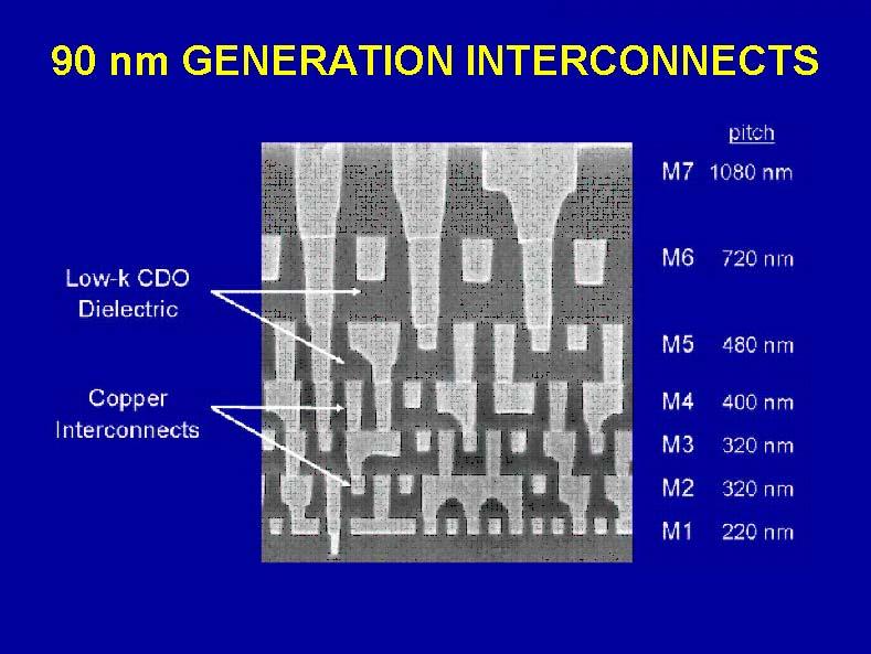
22 FEATURE SIZE TREND Micron um 2.0um 1.5um 1.0um.8um.5um.35um.25um.18um.13um 90nm 65nm 45nm 32nm Nanometer YEAR
23 MOSFET with PERFORMANCE BOOSTERS Strain / Stress Engineering to alter inter-atomic spacing in the channel region to improve mobility ( e.g., SiN overlayer, SiGe or Ge source/drain, Ge stressor, buried SiGe strain-transfer structure) Contact Resistance Engineering to reduce series resistance in source and drain regions to improve I Dsat ( e.g., metal-semiconductor barrier height adjustment, novel alloy silicides, Schottky-barrier source and drain ErSi 2 for NMOS, PtSi for PMOS) Gate Stack Engineering to eliminate gate depletion effect to increase gate capacitance ( e.g., dual metal-gate process, tuning metal-silicide work function)

24 EVOLUTION OF FinFET
25 5 nm P-TYPE/ 10 nm N-TYPE NANOWIRE FinFET
26 LOGIC DEVICE OPTIONS Carbon Nanotube Field-Effect Transistor (CNFET) difficulty in contacting small diameter CNTs difficulty in forming nanotubles with desired physical features and orientation difficulty in elimination of ambipolar conduction Molecular Devices limitation in operating temperature difficulty in making contacts to individual molecules Quantum-dot Cellular Automata (Single - Electron Parametron) limitation in operating temperature sensitivity to random background charge and low speed All above options suffer from parasitic capacitance and resistance which dominate device performances
27 FLOATING-GATE NONVOLATILE SEMICONDUCTOR MEMORY The floating-gate nonvolatile semiconductor memory (NVSM) is the most important memory device. NVSM family includes EPROM, EEPROM, and Flash Memory There are more NVSM cells produced in the world than any other semiconductor device (6x10 18 bites in 2007, i.e., more than 800 million bits for every person on earth) Flash Memory (NAND) is cheaper than DRAM, and its density is getting close to hard disk drive Two limiting cases of floating-gate NVSM: SONOS-when the thickness of the floating gate is reduced to zero, we have an MNOS memory ( and its new version, the SONOS) Nano-floating-gate memory when the length of the floating gate is reduced to 5-10 nm, we have a nanocrystal or nano-floating-gate memory
28
29 NONVOLATILE MEMORY OPTIONS MRAM (Magneto-resistive Random Access Memory) : based on tunneling Magnetoresistance effect FeRAM (Ferroelectric RAM) : based on remanent polarization in perovskite materials PCRAM (Phase-change RAM): based on reversible phase conversion between the amorphous and the crystalline state of a chalcogenide glass, which is accomplished by heating and cooling of the glass RRAM (Resistance RAM) : based on change in resistance with applied electric field Polymer Memory : based on resistance change of polymer at cross point of metal layers Millipede Memory : based on concept similar to punch cards, using thermally assisted, rewritable displacement media such as PMMA
30 INTERCONNECT CHALLENGES Low parasitic R and C to improve circuit speed Low power dissipation (power~cv 2 ) Scaling limit of multilevel interconnect System-on-chip, network-on-chip, superchip to minimize interconnect length Interconnect options at sub-25nm regime
31 45
32 3G/4G
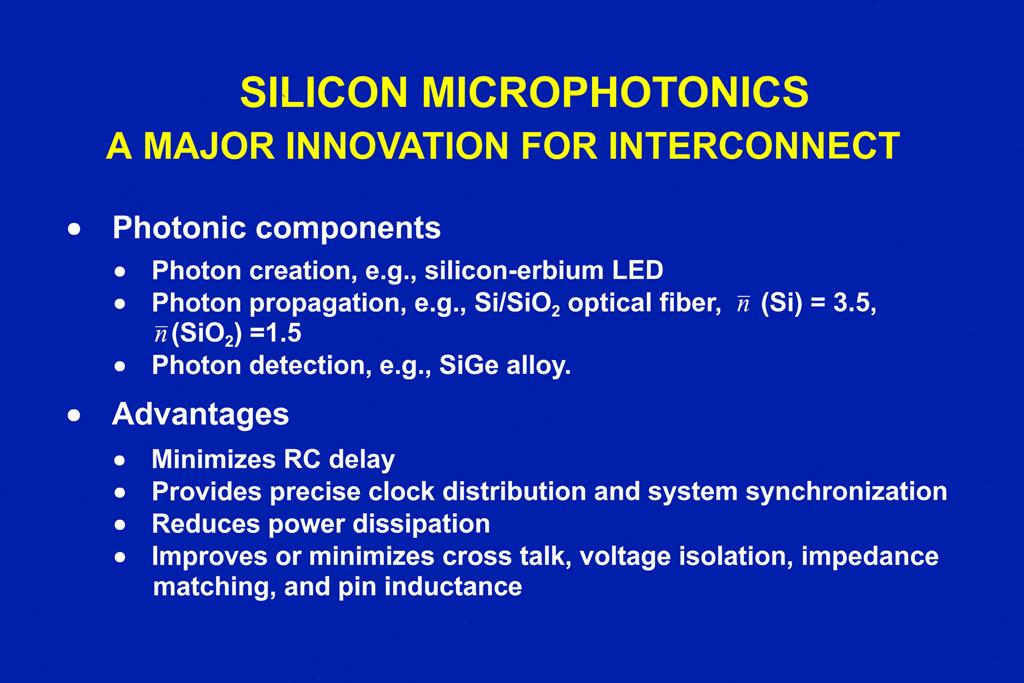
33 INTERCONNECT OPTIONS At Sub-25nm REGIME Metallic Carbon Nanotuble ( Single Wall or Multi-wall) long mean free path ( >1 µm, 100 times of Cu) and low resistivity (5 µω cm) can sustain current density >10 9 A/cm 2 (100 times of Cu) Conducting Polymer may be useful for molecular electronic Metallized DNA may be useful for DNA template for self-assembly Metallic Nanowire low resistivity can sustain current density >10 8 A/cm 2 Silicon Microphotonics
34
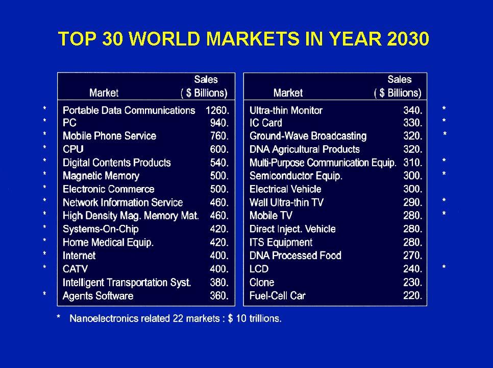
35 ECONOMIC CHALLENGES Skyrocketing wafer fab cost 500 time increase since 1975 : $6M (1975), $3B (2005), ~$10B (2020) Innovative processes needed to lower manufacturing cost New applications will broaden electronic market By 2030, semiconductor industry may reach $1.6 trillions By 2030, electronic industry may reach $10 trillions and constitutes 10% of Gross World Product

36 METRIC OF PROGRESS For Marine Turbines and Jet Passenger Aircraft
37 METRIC OF PROGRESS (CONTINUED) For marine turbines: shaft Horsepower has been flat since 1942 For jet passenger aircraft: people momentum has been flat since 1979 But the marine and aircraft industries have diversified. There is a proliferation of types of ship and aircraft, carefully chosen for specific applications. The discriminators now are fuel efficiency, in-cabin or in-flight comfort, and ecological friendliness of the ship or aircraft For nanoelectronics: The Moore s Law. But the diversification has already begun. For example, the raw computing power is secondary to the range of applications and services that can be provided by a single cellular phone
38
39 CONCLUSION In the past five decades, microelectronics has been responsible for the rapid growth of the global electronic industry which is now the largest industry in the world ( > $ 2 trillions ) There are many major challenges in nanoelectronics: large wafer, sub-100 nm lithography, deca-nano devices, interconnect, and economic challenges Super-large-diameter wafers will be adopted as long as the production cost per unit area can be reduced The 193 nm ArF system with immersion lens can support the 45 nm technology node. We may need EUV systems for sub-25nm technology nodes
40 CONCLUSION (CONTINUED) The ultimate logic device will be the MOSFET with performance boosters, and the ultimate memory device will be a nonvolatile memory ( possibly a member of the floating-gate family) IC performance will be limited by interconnect. For sub-25um ICs, two options are the metallic CNT and the silicon microphotonics Low-cost manufacturing processes and broadened electronic applications will support the growth of the nanoelectronics The electronic industry will remain to be the largest industry in the world for the next five to ten decades. However, we must develop innovative nanoelectronic technologies to meet the aforementioned challenges
Intel's 65 nm Logic Technology Demonstrated on 0.57 µm 2 SRAM Cells
 Intel's 65 nm Logic Technology Demonstrated on 0.57 µm 2 SRAM Cells Mark Bohr Intel Senior Fellow Director of Process Architecture & Integration Intel 1 What are We Announcing? Intel has fabricated fully-functional
New Process Technologies Will silicon CMOS carry us to the end of the Roadmap?
 HPEC Workshop 2006 New Process Technologies Will silicon CMOS carry us to the end of the Roadmap? Craig L. Keast, Chenson Chen, Mike Fritze, Jakub Kedzierski, Dave Shaver HPEC 2006-1 Outline A brief history
Lecture 33 - The Short Metal-Oxide-Semiconductor Field-Effect Transistor (cont.) April 30, 2007
 April 30, 2007") 6.720J/3.43J - Integrated Microelectronic Devices - Spring 2007 Lecture 33-1 Lecture 33 - The Short Metal-Oxide-Semiconductor Field-Effect Transistor (cont.) April 30, 2007 Contents: 1. MOSFET scaling
6.720J/3.43J - Integrated Microelectronic Devices - Spring 2007 Lecture 33-1 Lecture 33 - The Short Metal-Oxide-Semiconductor Field-Effect Transistor (cont.) April 30, 2007 Contents: 1. MOSFET scaling
The future of lithography and its impact on design
 The future of lithography and its impact on design Chris Mack www.lithoguru.com 1 Outline History Lessons Moore s Law Dennard Scaling Cost Trends Is Moore s Law Over? Litho scaling? The Design Gap The
Transistor Scaling in the Innovation Era. Mark Bohr Intel Senior Fellow Logic Technology Development August 15, 2011
 Transistor Scaling in the Innovation Era Mark Bohr Intel Senior Fellow Logic Technology Development August 15, 2011 MOSFET Scaling Device or Circuit Parameter Scaling Factor Device dimension tox, L, W
Newer process technology (since 1999) includes :
 includes :") Newer process technology (since 1999) includes : copper metalization hi-k dielectrics for gate insulators si on insulator strained silicon lo-k dielectrics for interconnects Immersion lithography for masks
Newer process technology (since 1999) includes : copper metalization hi-k dielectrics for gate insulators si on insulator strained silicon lo-k dielectrics for interconnects Immersion lithography for masks
Semiconductor Memory: DRAM and SRAM. Department of Electrical and Computer Engineering, National University of Singapore
 Semiconductor Memory: DRAM and SRAM Outline Introduction Random Access Memory (RAM) DRAM SRAM Non-volatile memory UV EPROM EEPROM Flash memory SONOS memory QD memory Introduction Slow memories Magnetic
Introduction to Electronic Devices
 (Course Number 300331) Fall 2006 Instructor: Dr. Dietmar Knipp Assistant Professor of Electrical Engineering Information: http://www.faculty.iubremen.de/dknipp/ Source: Apple Ref.: Apple Ref.: IBM Critical
ISSCC 2003 / SESSION 1 / PLENARY / 1.1
 ISSCC 2003 / SESSION 1 / PLENARY / 1.1 1.1 No Exponential is Forever: But Forever Can Be Delayed! Gordon E. Moore Intel Corporation Over the last fifty years, the solid-state-circuits industry has grown
Advanced Digital Integrated Circuits. Lecture 2: Scaling Trends. Announcements. No office hour next Monday. Extra office hour Tuesday 2-3pm
 EE241 - Spring 20 Advanced Digital Integrated Circuits Lecture 2: Scaling Trends and Features of Modern Technologies Announcements No office hour next Monday Extra office hour Tuesday 2-3pm 2 1 Outline
ITRS MOSFET Scaling Trends, Challenges, and Key Technology Innovations
 Workshop on Frontiers of Extreme Computing Santa Cruz, CA October 24, 2005 ITRS MOSFET Scaling Trends, Challenges, and Key Technology Innovations Peter M. Zeitzoff Outline Introduction MOSFET scaling and
Lecture #29. Moore s Law
 Lecture #29 ANNOUNCEMENTS HW#15 will be for extra credit Quiz #6 (Thursday 5/8) will include MOSFET C-V No late Projects will be accepted after Thursday 5/8 The last Coffee Hour will be held this Thursday
Enabling Breakthroughs In Technology
 Enabling Breakthroughs In Technology Mike Mayberry Director of Components Research VP, Technology and Manufacturing Group Intel Corporation June 2011 Defined To be defined Enabling a Steady Technology
write-nanocircuits Direct-write Jaebum Joo and Joseph M. Jacobson Molecular Machines, Media Lab Massachusetts Institute of Technology, Cambridge, MA
 Fab-in in-a-box: Direct-write write-nanocircuits Jaebum Joo and Joseph M. Jacobson Massachusetts Institute of Technology, Cambridge, MA April 17, 2008 Avogadro Scale Computing / 1 Avogadro number s? Intel
Opportunities and Challenges for Nanoelectronic Devices and Processes
 The Sixth U.S.-Korea Forum on Nanotechnology, April 28-29, 2009, Las Vegas, NV Opportunities and Challenges for Nanoelectronic Devices and Processes Yoshio Nishi Professor, Electrical Engineering, Material
Trends and Challenges in VLSI Technology Scaling Towards 100nm
 Trends and Challenges in VLSI Technology Scaling Towards 100nm Stefan Rusu Intel Corporation stefan.rusu@intel.com September 2001 Stefan Rusu 9/2001 2001 Intel Corp. Page 1 Agenda VLSI Technology Trends
Fin-Shaped Field Effect Transistor (FinFET) Min Ku Kim 03/07/2018
 Min Ku Kim 03/07/2018") Fin-Shaped Field Effect Transistor (FinFET) Min Ku Kim 03/07/2018 ECE 658 Sp 2018 Semiconductor Materials and Device Characterizations OUTLINE Background FinFET Future Roadmap Keeping up w/ Moore s Law
Fin-Shaped Field Effect Transistor (FinFET) Min Ku Kim 03/07/2018 ECE 658 Sp 2018 Semiconductor Materials and Device Characterizations OUTLINE Background FinFET Future Roadmap Keeping up w/ Moore s Law
Scaling of Semiconductor Integrated Circuits and EUV Lithography
 Scaling of Semiconductor Integrated Circuits and EUV Lithography ( 半導体集積回路の微細化と EUV リソグラフィー ) December 13, 2016 EIDEC (Emerging nano process Infrastructure Development Center, Inc.) Hidemi Ishiuchi 1 OUTLINE
ECE 5745 Complex Digital ASIC Design Topic 2: CMOS Devices
 ECE 5745 Complex Digital ASIC Design Topic 2: CMOS Devices Christopher Batten School of Electrical and Computer Engineering Cornell University http://www.csl.cornell.edu/courses/ece5950 Simple Transistor
HOW TO CONTINUE COST SCALING. Hans Lebon
 HOW TO CONTINUE COST SCALING Hans Lebon OUTLINE Scaling & Scaling Challenges Imec Technology Roadmap Wafer size scaling : 450 mm 2 COST SCALING IMPROVED PERFORMANCE 3 GLOBAL TRAFFIC FORECAST Cloud Traffic
Design of low threshold Full Adder cell using CNTFET
 Design of low threshold Full Adder cell using CNTFET P Chandrashekar 1, R Karthik 1, O Koteswara Sai Krishna 1 and Ardhi Bhavana 1 1 Department of Electronics and Communication Engineering, MLR Institute
Practical Information
 EE241 - Spring 2013 Advanced Digital Integrated Circuits MW 2-3:30pm 540A/B Cory Practical Information Instructor: Borivoje Nikolić 509 Cory Hall, 3-9297, bora@eecs Office hours: M 11-12, W 3:30pm-4:30pm
Innovation to Advance Moore s Law Requires Core Technology Revolution
 Innovation to Advance Moore s Law Requires Core Technology Revolution Klaus Schuegraf, Ph.D. Chief Technology Officer Silicon Systems Group Applied Materials UC Berkeley Seminar March 9 th, 2012 Innovation
450mm and Moore s Law Advanced Packaging Challenges and the Impact of 3D
 450mm and Moore s Law Advanced Packaging Challenges and the Impact of 3D Doug Anberg VP, Technical Marketing Ultratech SOKUDO Lithography Breakfast Forum July 10, 2013 Agenda Next Generation Technology
Progress due to: Feature size reduction - 0.7X/3 years (Moore s Law). Increasing chip size - 16% per year. Creativity in implementing functions.
. Increasing chip size - 16% per year. Creativity in implementing functions.") Introduction - Chapter 1 Evolution of IC Fabrication 1960 and 1990 integrated t circuits. it Progress due to: Feature size reduction - 0.7X/3 years (Moore s Law). Increasing chip size - 16% per year. Creativity
Introduction - Chapter 1 Evolution of IC Fabrication 1960 and 1990 integrated t circuits. it Progress due to: Feature size reduction - 0.7X/3 years (Moore s Law). Increasing chip size - 16% per year. Creativity
Practical Information
 EE241 - Spring 2010 Advanced Digital Integrated Circuits TuTh 3:30-5pm 293 Cory Practical Information Instructor: Borivoje Nikolić 550B Cory Hall, 3-9297, bora@eecs Office hours: M 10:30am-12pm Reader:
Nanoelectronics and the Future of Microelectronics
 Nanoelectronics and the Future of Microelectronics Mark Lundstrom Electrical and Computer Engineering University, West Lafayette, IN August 22, 2002 1. Introduction 2. Challenges in Silicon Technology
Nanometer Technologies: Where Design and Manufacturing Converge. Walden C. Rhines CHAIRMAN & CEO
 Nanometer Technologies: Where Design and Manufacturing Converge Walden C. Rhines CHAIRMAN & CEO Nanometer Technologies: Where Design and Manufacturing Converge Nanometer technologies make designers aware
Research Needs for Device Sciences Modeling and Simulation (May 6, 2005)
") Research Needs for Device Sciences Modeling and Simulation (May 6, 2005) SRC Device Sciences 2005 Modeling and Simulation Task Force Contributing organizations: Axcelis, Freescale, IBM, Intel, LSI, SRC,
Research Needs for Device Sciences Modeling and Simulation (May 6, 2005) SRC Device Sciences 2005 Modeling and Simulation Task Force Contributing organizations: Axcelis, Freescale, IBM, Intel, LSI, SRC,
Chapter 2 : Semiconductor Materials & Devices (II) Feb
 Feb") Chapter 2 : Semiconductor Materials & Devices (II) 1 Reference 1. SemiconductorManufacturing Technology: Michael Quirk and Julian Serda (2001) 3. Microelectronic Circuits (5/e): Sedra & Smith (2004) 4.
Chapter 2 : Semiconductor Materials & Devices (II) 1 Reference 1. SemiconductorManufacturing Technology: Michael Quirk and Julian Serda (2001) 3. Microelectronic Circuits (5/e): Sedra & Smith (2004) 4.
MICROPROCESSOR TECHNOLOGY
 MICROPROCESSOR TECHNOLOGY Assis. Prof. Hossam El-Din Moustafa Lecture 3 Ch.1 The Evolution of The Microprocessor 17-Feb-15 1 Chapter Objectives Introduce the microprocessor evolution from transistors to
Alternatives to standard MOSFETs. What problems are we really trying to solve?
 Alternatives to standard MOSFETs A number of alternative FET schemes have been proposed, with an eye toward scaling up to the 10 nm node. Modifications to the standard MOSFET include: Silicon-in-insulator
Chapter 15 Summary and Future Trends
 Chapter 15 Summary and Future Trends Hong Xiao, Ph. D. hxiao89@hotmail.com www2.austin.cc.tx.us/hongxiao/book.htm Hong Xiao, Ph. D. www2.austin.cc.tx.us/hongxiao/book.htm 1 The 1960s First IC product Bipolar
TWINSCAN XT:1950i Water-based immersion taken to the max Enabling fast, single-exposure lithography at sub 40 nm
 TWINSCAN XT:1950i Water-based immersion taken to the max Enabling fast, single-exposure lithography at sub 40 nm SEMICON West, San Francisco July 14-18, 2008 Slide 1 The immersion pool becomes an ocean
Thermal Management in the 3D-SiP World of the Future
 Thermal Management in the 3D-SiP World of the Future Presented by W. R. Bottoms March 181 th, 2013 Smaller, More Powerful Portable Devices Are Driving Up Power Density Power (both power delivery and power
State-of-the-art device fabrication techniques
 State-of-the-art device fabrication techniques! Standard Photo-lithography and e-beam lithography! Advanced lithography techniques used in semiconductor industry Deposition: Thermal evaporation, e-gun
Intel s s Silicon Power Savings Strategy
 Intel s s Silicon Power Savings Strategy Keeping Moore s s Law Alive and Well Paolo Gargini Intel Fellow and Director, Technology Strategy Agenda Moore s s Law and scaling The power challenge Looking ahead
EECS 151/251A Spring 2019 Digital Design and Integrated Circuits. Instructors: Wawrzynek. Lecture 8 EE141
 EECS 151/251A Spring 2019 Digital Design and Integrated Circuits Instructors: Wawrzynek Lecture 8 EE141 From the Bottom Up IC processing CMOS Circuits (next lecture) EE141 2 Overview of Physical Implementations
Outline. Introduction on IMEC & IMEC cooperation model. Program Challenges in CMOS scaling
 imec 2009 1 The Role of European Research Institutes in the 450mm Wafer Transition Process IMEC nanoelectronics platform A Collaborative approach towards 450mm R&D IMEC March 2009 Outline Introduction
EE4800 CMOS Digital IC Design & Analysis. Lecture 1 Introduction Zhuo Feng
 EE4800 CMOS Digital IC Design & Analysis Lecture 1 Introduction Zhuo Feng 1.1 Prof. Zhuo Feng Office: EERC 730 Phone: 487-3116 Email: zhuofeng@mtu.edu Class Website http://www.ece.mtu.edu/~zhuofeng/ee4800fall2010.html
FinFET vs. FD-SOI Key Advantages & Disadvantages
 FinFET vs. FD-SOI Key Advantages & Disadvantages Amiad Conley Technical Marketing Manager Process Diagnostics & Control, Applied Materials ChipEx-2014, Apr 2014 1 Moore s Law The number of transistors
Integrated Circuit Technology (Course Code: EE662) Lecture 1: Introduction
 Lecture 1: Introduction") Indian Institute of Technology Jodhpur, Year 2015 2016 Integrated Circuit Technology (Course Code: EE662) Lecture 1: Introduction Course Instructor: Shree Prakash Tiwari, Ph.D. Email: sptiwari@iitj.ac.in
Indian Institute of Technology Jodhpur, Year 2015 2016 Integrated Circuit Technology (Course Code: EE662) Lecture 1: Introduction Course Instructor: Shree Prakash Tiwari, Ph.D. Email: sptiwari@iitj.ac.in
Multiple Patterning for Immersion Extension and EUV Insertion. Chris Bencher Distinguished Member of Technical Staff Applied Materials CTO group
 Multiple Patterning for Immersion Extension and EUV Insertion Chris Bencher Distinguished Member of Technical Staff Applied Materials CTO group Abstract Multiple Patterning for Immersion Extension and
Future Challenges and Needs for Nano- Electronics from Manufacturing View Point
 First International Symposium on Nano-manufacturing, April 24-26, 2003 Future Challenges and Needs for Nano- Electronics from Manufacturing View Point Yoshio Nishi Stanford Nanofabrication Facility Department
Introduction to Materials Engineering: Materials Driving the Electronics Revolution Robert Hull, MSE
 Introduction to Materials Engineering: Materials Driving the Electronics Revolution Robert Hull, MSE Outline Microelectronics Miniaturization Historical Development: Electronics before Semiconductors The
Packaging Roadmap: The impact of miniaturization. Bob Pfahl, inemi Celestica-iNEMI Technology Forum May 15, 2007
 Packaging Roadmap: The impact of miniaturization Bob Pfahl, inemi Celestica-iNEMI Technology Forum May 15, 2007 The Challenges for the Next Decade Addressing the consumer experience using the converged
Towards a Reconfigurable Nanocomputer Platform
 Towards a Reconfigurable Nanocomputer Platform Paul Beckett School of Electrical and Computer Engineering RMIT University Melbourne, Australia 1 The Nanoscale Cambrian Explosion Disparity: Widerangeof
Nanotechnology, the infrastructure, and IBM s research projects
 Nanotechnology, the infrastructure, and IBM s research projects Dr. Paul Seidler Coordinator Nanotechnology Center, IBM Research - Zurich Nanotechnology is the understanding and control of matter at dimensions
EE241 - Spring 2013 Advanced Digital Integrated Circuits. Announcements. Sign up for Piazza if you haven t already
 EE241 - Spring 2013 Advanced Digital Integrated Circuits Lecture 2: Scaling Trends and Features of Modern Technologies Announcements Sign up for Piazza if you haven t already 2 1 Assigned Reading R.H.
PUSHING LITHOGRAPHY TO ENABLE ULTIMATE NANO-ELECTRONICS. LUC VAN DEN HOVE President & CEO imec
 PUSHING LITHOGRAPHY TO ENABLE ULTIMATE NANO-ELECTRONICS LUC VAN DEN HOVE President & CEO imec OUTLINE! Industry drivers! Roadmap extension! Lithography options! Innovation through global collaboration
CS4617 Computer Architecture
 1/26 CS4617 Computer Architecture Lecture 2 Dr J Vaughan September 10, 2014 2/26 Amdahl s Law Speedup = Execution time for entire task without using enhancement Execution time for entire task using enhancement
32nm Technology and Beyond
 32nm Technology and Beyond Paolo Gargini Chairman ITRS IEEE Fellow Director of Technology Strategy Intel Fellow ISS Europe 2009 P. Gargini 1 Agenda Equivalent Scaling 45nm Technology summary 32nm Technology
FOR SEMICONDUCTORS 2009 EDITION
 INTERNATIONAL TECHNOLOGY ROADMAP FOR SEMICONDUCTORS 2009 EDITION PROCESS INTEGRATION, DEVICES, AND STRUCTURES THE ITRS IS DEVISED AND INTENDED FOR TECHNOLOGY ASSESSMENT ONLY AND IS WITHOUT REGARD TO ANY
420 Intro to VLSI Design
 Dept of Electrical and Computer Engineering 420 Intro to VLSI Design Lecture 0: Course Introduction and Overview Valencia M. Joyner Spring 2005 Getting Started Syllabus About the Instructor Labs, Problem
Selected Topics in Nanoelectronics. Danny Porath 2002
 Selected Topics in Nanoelectronics Danny Porath 2002 Links to NST http://www.foresight.org/ http://itri.loyola.edu/nanobase/ http://www.zyvex.com/nano/ http://www.nano.gov/ http://www.aeiveos.com/nanotech/
ATV 2011: Computer Engineering
 ATV 2011: Technology Trends in Computer Engineering Professor Per Larsson-Edefors ATV 2011, L1, Per Larsson-Edefors Page 1 Solid-State Devices www.cse.chalmers.se/~perla/ugrad/ SemTech/Lectures_2000.pdf
Chapter 3: Basics Semiconductor Devices and Processing 2006/9/27 1. Topics
 Chapter 3: Basics Semiconductor Devices and Processing 2006/9/27 1 Topics What is semiconductor Basic semiconductor devices Basics of IC processing CMOS technologies 2006/9/27 2 1 What is Semiconductor
Part II: The MOS Transistor Technology. J. SÉE 2004/2005
 Part II: The MOS Transistor Technology J. SÉE johann.see@ief.u-psud.fr 2004/2005 Lecture plan Towards the nanotechnologies... data storage The data processing through the ages MOS transistor in logic-gates
FUTURE PROSPECTS FOR CMOS ACTIVE PIXEL SENSORS
 FUTURE PROSPECTS FOR CMOS ACTIVE PIXEL SENSORS Dr. Eric R. Fossum Jet Propulsion Laboratory Dr. Philip H-S. Wong IBM Research 1995 IEEE Workshop on CCDs and Advanced Image Sensors April 21, 1995 CMOS APS
Limitations and Challenges to Meet Moore's Law
 Limitations and Challenges to Meet Moore's Law Sept 10, 2015 Sung Kim sung_kim@amat.com State of the art: cleanroom toolsets metrology analysis module development test & reliability Introduction Why do
CMOL: Hybrid of CMOS with Overlaid Nanogrid and Nanodevice Structure. John Zacharkow
 CMOL: Hybrid of CMOS with Overlaid Nanogrid and Nanodevice Structure John Zacharkow Overview Introduction Background CMOS Review CMOL Breakdown Benefits/Shortcoming Looking into the Future Introduction
Nano-crystalline Oxide Semiconductor Materials for Semiconductor and Display Technology Sanghun Jeon Ph.D. Associate Professor
 Nano-crystalline Oxide Semiconductor Materials for Semiconductor and Display Technology Sanghun Jeon Ph.D. Associate Professor Department of Applied Physics Korea University Personnel Profile (Affiliation
A 90 nm High Volume Manufacturing Logic Technology Featuring Novel 45 nm Gate Length Strained Silicon CMOS Transistors
 A 90 nm High Volume Manufacturing Logic Technology Featuring Novel 45 nm Gate Length Strained Silicon CMOS Transistors T. Ghani, M. Armstrong, C. Auth, M. Bost, P. Charvat, G. Glass, T. Hoffmann*, K. Johnson#,
Non-Volatile Memory Characterization and Measurement Techniques
 Non-Volatile Memory Characterization and Measurement Techniques Alex Pronin Keithley Instruments, Inc. 1 2012-5-21 Why do more characterization? NVM: Floating gate Flash memory Very successful; lead to
Sub-micron technology IC fabrication process trends SOI technology. Development of CMOS technology. Technology problems due to scaling
 Goodbye Microelectronics Welcome Nanoelectronics Sub-micron technology IC fabrication process trends SOI technology SiGe Tranzistor in 50nm process Virus The thickness of gate oxide= 1.2 nm!!! Today we
Drain. Drain. [Intel: bulk-si MOSFETs]
![Drain. Drain. [Intel: bulk-si MOSFETs]](/thumbs/89/97695223.jpg "Drain. Drain. [Intel: bulk-si MOSFETs]") 1 Introduction For more than 40 years, the evolution and growth of very-large-scale integration (VLSI) silicon-based integrated circuits (ICs) have followed from the continual shrinking, or scaling, of
1 Introduction For more than 40 years, the evolution and growth of very-large-scale integration (VLSI) silicon-based integrated circuits (ICs) have followed from the continual shrinking, or scaling, of
Chapter 3 Basics Semiconductor Devices and Processing
 Chapter 3 Basics Semiconductor Devices and Processing 1 Objectives Identify at least two semiconductor materials from the periodic table of elements List n-type and p-type dopants Describe a diode and
CMOS Technology & Business Trends
 CMOS Technology & Business Trends Can the semiconductor industry afford to continue advancing? Peter M. O Neill Automated Test Innovations Agilent Laboratories Disclaimers Not a thoroughly researched paper
Lecture 1 Introduction to Solid State Electronics
 EE 471: Transport Phenomena in Solid State Devices Spring 2018 Lecture 1 Introduction to Solid State Electronics Bryan Ackland Department of Electrical and Computer Engineering Stevens Institute of Technology
Challenges and Innovations in Nano CMOS Transistor Scaling
 Challenges and Innovations in Nano CMOS Transistor Scaling Tahir Ghani Intel Fellow Logic Technology Development October, 2009 Nikkei Presentation 1 Outline Traditional Scaling Traditional Scaling Limiters,
Memory (Part 1) RAM memory
 RAM memory") Budapest University of Technology and Economics Department of Electron Devices Technology of IT Devices Lecture 7 Memory (Part 1) RAM memory Semiconductor memory Memory Overview MOS transistor recap and
Budapest University of Technology and Economics Department of Electron Devices Technology of IT Devices Lecture 7 Memory (Part 1) RAM memory Semiconductor memory Memory Overview MOS transistor recap and
Design of Nano-Electro Mechanical (NEM) Relay Based Nano Transistor for Power Efficient VLSI Circuits
 Relay Based Nano Transistor for Power Efficient VLSI Circuits") Design of Nano-Electro Mechanical (NEM) Relay Based Nano Transistor for Power Efficient VLSI Circuits Arul C 1 and Dr. Omkumar S 2 1 Research Scholar, SCSVMV University, Kancheepuram, India. 2 Associate
Design of Nano-Electro Mechanical (NEM) Relay Based Nano Transistor for Power Efficient VLSI Circuits Arul C 1 and Dr. Omkumar S 2 1 Research Scholar, SCSVMV University, Kancheepuram, India. 2 Associate
Introduction to VLSI ASIC Design and Technology
 Introduction to VLSI ASIC Design and Technology Paulo Moreira CERN - Geneva, Switzerland Paulo Moreira Introduction 1 Outline Introduction Is there a limit? Transistors CMOS building blocks Parasitics
Intel Technology Journal
 Volume 06 Issue 02 Published, May 16, 2002 ISSN 1535766X Intel Technology Journal Semiconductor Technology and Manufacturing The Intel Lithography Roadmap A compiled version of all papers from this issue
32nm High-K/Metal Gate Version Including 2nd Generation Intel Core processor family
 From Sand to Silicon Making of a Chip Illustrations 32nm High-K/Metal Gate Version Including 2nd Generation Intel Core processor family April 2011 1 The illustrations on the following foils are low resolution
Homework 10 posted just for practice. Office hours next week, schedule TBD. HKN review today. Your feedback is important!
 EE141 Fall 2005 Lecture 26 Memory (Cont.) Perspectives Administrative Stuff Homework 10 posted just for practice No need to turn in Office hours next week, schedule TBD. HKN review today. Your feedback
Parameter Optimization Of GAA Nano Wire FET Using Taguchi Method
 Parameter Optimization Of GAA Nano Wire FET Using Taguchi Method S.P. Venu Madhava Rao E.V.L.N Rangacharyulu K.Lal Kishore Professor, SNIST Professor, PSMCET Registrar, JNTUH Abstract As the process technology
VLSI: An Introduction
 Chapter 1 UEEA2223/UEEG4223 Integrated Circuit Design VLSI: An Introduction Prepared by Dr. Lim Soo King 02 Jan 2011. Chapter 1 VLSI Design: An Introduction... 1 1.0 Introduction... 1 1.0.1 Early Computing
Introduction. Digital Integrated Circuits A Design Perspective. Jan M. Rabaey Anantha Chandrakasan Borivoje Nikolic. July 30, 2002
 Digital Integrated Circuits A Design Perspective Jan M. Rabaey Anantha Chandrakasan Borivoje Nikolic Introduction July 30, 2002 1 What is this book all about? Introduction to digital integrated circuits.
EMT 251 Introduction to IC Design
 EMT 251 Introduction to IC Design (Pengantar Rekabentuk Litar Terkamir) Semester II 2011/2012 Introduction to IC design and Transistor Fundamental Some Keywords! Very-large-scale-integration (VLSI) is
The Development of the Semiconductor CVD and ALD Requirement
 The Development of the Semiconductor CVD and ALD Requirement 1 Linx Consulting 1. We create knowledge and develop unique insights at the intersection of electronic thin film processes and the chemicals
Intel Xeon E3-1230V2 CPU Ivy Bridge Tri-Gate 22 nm Process
 Intel Xeon E3-1230V2 CPU Structural Analysis 3685 Richmond Road, Suite 500, Ottawa, ON K2H 5B7 Canada Tel: 613-829-0414 www.chipworks.com Structural Analysis Some of the information in this report may
IC Knowledge LLC, PO Box 20, Georgetown, MA Ph: (978) , Fx: (978)
 , Fx: (978)") IC Knowledge LLC, PO Box 20, Georgetown, MA 01833 www.icknowledge.com Ph: (978) 352 7610, Fx: (978) 352 3870 Linx Consulting, PO Box 384, Mendon, MA 01756 0384 www.linxconsulting.com Ph: (617) 273 8837
IC Knowledge LLC, PO Box 20, Georgetown, MA 01833 www.icknowledge.com Ph: (978) 352 7610, Fx: (978) 352 3870 Linx Consulting, PO Box 384, Mendon, MA 01756 0384 www.linxconsulting.com Ph: (617) 273 8837
Implementation of Mod-16 Counter using Verilog-A Model of CNTFET
 Technology Volume 1, Issue 2, October-December, 2013, pp. 30-36, IASTER 2013 www.iaster.com, Online: 2347-6109, Print: 2348-0017 ABSTRACT Implementation of Mod-16 Counter using Verilog-A Model of CNTFET
Architecture of Computers and Parallel Systems Part 9: Digital Circuits
 Architecture of Computers and Parallel Systems Part 9: Digital Circuits Ing. Petr Olivka petr.olivka@vsb.cz Department of Computer Science FEI VSB-TUO Architecture of Computers and Parallel Systems Part
Simulation and Analysis of CNTFETs based Logic Gates in HSPICE
 Simulation and Analysis of CNTFETs based Logic Gates in HSPICE Neetu Sardana, 2 L.K. Ragha M.E Student, 2 Guide Electronics Department, Terna Engineering College, Navi Mumbai, India Abstract Conventional
Analysis and Processing of Power Output Signal of 200V Power Devices
 doi: 10.14355/ie.2015.03.005 Analysis and Processing of Power Output Signal of 200V Power Devices Cheng-Yen Wu 1, Hsin-Chiang You* 2, Chen-Chung Liu 3, Wen-Luh Yang 4 1 Ph.D. Program of Electrical and
Advanced PDK and Technologies accessible through ASCENT
 Advanced PDK and Technologies accessible through ASCENT MOS-AK Dresden, Sept. 3, 2018 L. Perniola*, O. Rozeau*, O. Faynot*, T. Poiroux*, P. Roseingrave^ olivier.faynot@cea.fr *Cea-Leti, Grenoble France;
IFSIN. WEB PAGE Fall ://weble.upc.es/ifsin/
 IFSIN IMPLEMENTACIÓ FÍSICA DE SISTEMES INTEGRATS NANOMÈTRICS IMPLEMENTACIÓN N FÍSICA F DE SISTEMAS INTEGRADOS NANOMÉTRICOS PHYSICAL IMPLEMENTATION OF NANOMETER INTEGRATED SYSTEMS Fall 2008 Prof. Xavier
Technological Challenges in Semiconductor Lithography
 Technological Challenges in Semiconductor Lithography some aspects of projection lithography technology and its position in high tech industry and academia Ramin Badie ASML Research 2014 What do I want
A Review of Low-Power VLSI Technology Developments
 A Review of Low-Power VLSI Technology Developments Nakka Ravi Kumar Abstract Ever since the invention of integrated circuits, there has been a continuous demand for high-performance, low-power, and low-area/low-cost
Section 2: Lithography. Jaeger Chapter 2 Litho Reader. The lithographic process
 Section 2: Lithography Jaeger Chapter 2 Litho Reader The lithographic process Photolithographic Process (a) (b) (c) (d) (e) (f) (g) Substrate covered with silicon dioxide barrier layer Positive photoresist
Section 2: Lithography. Jaeger Chapter 2. EE143 Ali Javey Slide 5-1
 Section 2: Lithography Jaeger Chapter 2 EE143 Ali Javey Slide 5-1 The lithographic process EE143 Ali Javey Slide 5-2 Photolithographic Process (a) (b) (c) (d) (e) (f) (g) Substrate covered with silicon
Comparison of 32nm High-k Metal Gate Predictive Technology Model CMOS and MOSFET-Like CNFET compact Model Based Domino logic Circuits
 Comparison of 32nm High-k Metal Gate Predictive Technology Model CMOS and MOSFET-Like CNFET compact Model Based Domino logic Circuits Saravana Maruthamuthu, Wireless Group Infineon Technologies India Private
SiNANO-NEREID Workshop:
 SiNANO-NEREID Workshop: Towards a new NanoElectronics Roadmap for Europe Leuven, September 11 th, 2017 WP3/Task 3.1: Nanoscale FET Anda Mocuta Introduction: technologies/concepts covered by the Roadmap
Section 2: Lithography. Jaeger Chapter 2 Litho Reader. EE143 Ali Javey Slide 5-1
 Section 2: Lithography Jaeger Chapter 2 Litho Reader EE143 Ali Javey Slide 5-1 The lithographic process EE143 Ali Javey Slide 5-2 Photolithographic Process (a) (b) (c) (d) (e) (f) (g) Substrate covered
III-V CMOS: Quo Vadis?
 III-V CMOS: Quo Vadis? J. A. del Alamo, X. Cai, W. Lu, A. Vardi, and X. Zhao Microsystems Technology Laboratories Massachusetts Institute of Technology Compound Semiconductor Week 2018 Cambridge, MA, May
Low-Power VLSI. Seong-Ook Jung VLSI SYSTEM LAB, YONSEI University School of Electrical & Electronic Engineering
 Low-Power VLSI Seong-Ook Jung 2013. 5. 27. sjung@yonsei.ac.kr VLSI SYSTEM LAB, YONSEI University School of Electrical & Electronic Engineering Contents 1. Introduction 2. Power classification & Power performance
LSI ON GLASS SUBSTRATES
 LSI ON GLASS SUBSTRATES OUTLINE Introduction: Why System on Glass? MOSFET Technology Low-Temperature Poly-Si TFT Technology System-on-Glass Technology Issues Conclusion System on Glass CPU SRAM DRAM EEPROM
Alternative Channel Materials for MOSFET Scaling Below 10nm
 Alternative Channel Materials for MOSFET Scaling Below 10nm Doug Barlage Electrical Requirements of Channel Mark Johnson Challenges With Material Synthesis Introduction Outline Challenges with scaling