Technological Challenges in Semiconductor Lithography
|
|
|
- Amberly Gregory
- 5 years ago
- Views:
Transcription


1 Technological Challenges in Semiconductor Lithography some aspects of projection lithography technology and its position in high tech industry and academia Ramin Badie ASML Research 2014
2 What do I want to share with you today Confidential Slide 2 17 February 2014 Share some general knowledge on the subject of projection lithography in the semiconductor industry from the standpoint of an ASML employee. Importance of engineering approach combined with academic knowledge in high tech industry using some examples from fluid dynamics and heat transfer in lithography tools. Some personal thoughts on the successes of ASML and its way of working in the lithography market. Discussion on the role of the high tech industry in the Netherlands.

3 Billion 50 Anything will be connected! that can benefit form connection THINGS Source: Ericsson, ISS Europe, Feb 2011 Inflection points for our industry PEOPLE PLACES
4 Integrated Circuits (chips) are integrated in our societal use Slide 4 16 October 2013
5 IC units, in billions Data: WSTS More than 180 billion chips are made every year Total IC units In 2012, 185 billion chips were produced 27 for every man, woman and child on the planet. Slide 5 16 October 2013


6 1947 The Point contact transistor Bell Labs How it all got started The First IC Texas Instruments 1961 The First Planar IC Fairchild
7 Slide 7

8 Lithography enables affordable connected electronics, improving quality of life and sustainability Slide 8 January 2013 $1,469 B Electronic Applications in 2012 $1,423 B in 2011, $1,343 B in 2010 $ 6.5 B Semiconductor Litho market in 2012 $8.2 B in 2011 $6.4 B in 2010 $297.6 B Semiconductor Chips in 2012 $306.8 B in 2011, $301.5 B in 2010 Source: Gartner Q4/12 and ASML
9 Driving the semiconductor industry: Moore s Statement Slide 9 16 October 2013 Gordon Moore (1965): Number of transistors per chip doubles every year. Later adjusted to two years, the trend has held for more than four decades.

 Gate: RMG-HKMG")


10 Device roadmaps support shrink ambitions nm 16-14nm 11-10nm 8-7nm Logic Memory: 0.08um2, SRAM Device: planar or FinFET (Intel) Gate: RMG-HKMG Channel: Si Strain: stressor Vdd: 0.8V Memory: 0.05um2 SRAM Device: FinFET, FDSOI Gate: RMG-HKMG Channel: Si; (Si)Ge Strain: stressor Vdd: 0.6V Memory: 0.03um2 SRAM Device: FinFET Gate: HKMG Channel: Si, Ge, IIIV Strain: stressor Vdd: 0.5V Memory: FBRAM, STT-RAM, >8TSRAM Device: Nanowire, TFET Gate: HKMG Channel: IIIV-Graphene DRAM Flash 38-32nm Memory: stacked MIM Peri: planar Array: 6F2, bwl Gate: poly/sio2 Channel: Si Vdd=1.35V 24-19nm hp 32-28nm Memory: stacked MIM Peri: planar HKMG Array: 6F2, bwl Gate: HKMG Channel: Si Vdd=1.2V 16-14nm hp Node: 26-22nm Memory: stacked MIM Peri: planar Array: 4F2, bbl, LBL, 1T1C(VFET) Gate: HKMG Channel: Si Vdd=1.1V 13-11nm hp Node: 18-15nm Memory: FBRAM, STT-RAM, RRAM Peri: planar Array: 4F2, 1T, 1T1R, 1T1MTJ(VFET) Gate: HKMG Channel: Si Vdd~1V < 10nm hp 4.5F - 6F2 asymm. cell Density: G Device: FG Source: IMEC, ASML TDC, June 2011 ONO or CG High-k FG FG STI 6F2 asymmetric cell 4F2 symmetric cell Density: G Device: dual-fg Slide 10 7F2 asymmetric cell 4F2 symmetric cell Density: G Device:: dual-fg, Intro to BiCS, Density: > 1T with 3D chip stacking Device: 3D BiCS, XPoint-RRAM Selector: diode
11 Moore s Statement makes chips cheaper Slide October $1,162 for 1 GB 1000 NAND Flash price $/GByte $0.17 for 1 GB Source: Gartner. High quality Flash
12 and more energy-efficient Computations per Kilowatt hour double every 1.5 years Slide October 2013 Computations per kwh 1.E+16 1.E+15 1.E+14 1.E+13 1.E+12 1.E+11 1.E+10 1.E+09 1.E+08 1.E+07 1.E+06 1.E+05 1.E+04 1.E+03 1.E+02 1.E+01 Univac I Eniac EDVAC SDS 920 IBM PC Cray 1 supercomputer DEC PDP-11/20 Univac II Univac III (transistors) Dell Dimension 2400 Gateway P MHz IBM PS/2E + Sun SS1000 IBM PC-AT IBM PC-XT Commodore laptops SiCortex SC5832 Dell Optiplex GXI 486/25 and 486/33 Desktops Regression results: N = 76 Adjusted R-squared = Comps/kWh = exp( x year ) Average doubling time (1946 to 2009) = 1.57 years 1.E Source: Jonathan Koomey, Lawrence Berkeley National Laboratory and Stanford University, 2009
13 Moore s statement means doing more with less Cray 1: The first supercomputer Slide October megabytes of memory 5.5 tons 150 kilowatt power supply Innovative Freon cooling system $8.8 million ($30 million in today s dollars) 1976

14 Moore s statement means doing more with less Slide October 2013 The supercomputer in your pocket: a fraction of the materials, price, power consumption


![Total 2004 Total Flash price 1 GB [$] 2005](/docs-images/81/83141916/images/15-5.jpg "Total 2006 Total 2007 Total 2008 Total 2009")
15 10 Cheaper chips drive market growth 1,000 Slide October 2013 MP3 player Flash units (in billions) Digital cameras Smart phones Solid state hard drives Flash price per GB (in dollars) Total flash units [B] Total 2001 Total 2002 Total 2003 Total 2004 Total Flash price 1 GB [$] 2005 Total 2006 Total 2007 Total 2008 Total 2009 Total 2010 Total 2011 Total 1
16 A virtuous cycle Slide October 2013


17 Everyday objects get connected Slide October 2013 GPS Fleet tracking Cash registers Smart meters Wireless IP camera
 Camera pill with camera, transmitter and computer DNA analysis")
 Lab on a Chip (LOC) for counting red blood")
18 New devices, new applications Slide October 2013 Gyroscope (UC Irvine) Wearable sensors (Holst Centre) Camera pill with camera, transmitter and computer DNA analysis (Affymetrix) Accelerometer (IC Mechanics) Micromirrors for beamers (TI) On-Chip DNA amplification and detection (imec/panasonic) Lab on a Chip (LOC) for counting red blood cells
19 Confidential Slide February 2014 About ASML

20 ASML provides lithography equipment to produce smaller and more powerful chips Slide 20 January 2013 The Semiconductor Manufacturing Process A variety of complementary suppliers provide the other tools, materials and packaging equipment necessary to make ICs


21 ASML makes machines for making chips Lithography is the critical tool for producing chips Slide October sales: 4.73 bln More than 70 offices in 16 countries More than employees (in FTEs, payroll and flexible contracts)
22 Founded in 1984 as a spin-off from Philips Slide February 2014

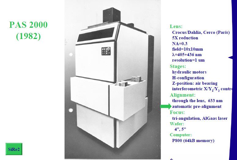
23 First Philips system operational in 1975 Lens: Tulipe, Cerco (Paris) 5X reduction NA=0.26 field=10x10mm λ=436 nm resolution= 2 um Stages: hydraulic wafer:x-direction lens: Y-direction interferometric X/Y control Alignment: through the lens Focus: air pressure Wafer: 3 and 4

24 17-Feb- Slide 24


25 resulting in the systems that conquered the market In 30 years: From 1,200 nm to less than 20 nm resolution From <0.5M per system to >60M 1984: PAS 2000 Resolution: >1µm overlay: 250 nm 1989: PAS 5000 Resolution: <500 nm overlay: 100 nm 1990 s: PAS 5500 steppers/scanners Resolution: 400 to 90 nm overlay: 100 to 12 nm Slide s: Twinscan Resolution: 100 to 38 nm overlay: 20 to 4 nm 2010 s: NXE EUV systems Resolution: 32 to <20 nm overlay: 2 nm
26 Key to Moore s Law: Making smaller transistors Slide October 2013 Transistor length has shrunk by a million The first integrated circuit on silicon, on a wafer the size of a fingernail (Fairchild Semiconductor, 1959) Today: More than a billion transistors on the same area (Intel, 2012)


27 The principle of Lithography Rayleigh equation: Resolution = k 1x λ NA Slide 27

28 Lithography is at the heart of chip manufacturing Repeat 30 to 40 times to build 3 dimensional structure / Slide 28
29 Chip has more than one layer Slide 29


30 The manufacturing loop Slide October 2013 Ion implantation Stripping Deposition Etching Developing Photoresist coating Exposure


31 Fluid thinking: the liquid lens scanner Lens Air Lens Water Slide 31


32 Main Cause Class Immersion defects Droplets Droplets Particles/ Droplets Standard catalogue, put together with customers Pattern expansion Drying stains Inverted attenuation Bubbles Pattern attenuation examples Main Cause Particles Process Develop Generic Class Printed particle Bridge Micro Bridge Missing Pattern Examples Slide 32
33 Immersion Research Program: Competence Build-up In co-operation with FOM, UT, TUD, TUE, and many other European universities, academia and research centers partly within EC funded project Advanced visualization techniques of flow and temperature in micro-layers in immersion tools Application of latest theories in contact line dynamics, wetting and dewetting to immersion lithography parameters Latest theories in surface chemistry applied to immersion parameters Development of up-to-date models for understanding and better solution finding of phenomena in immersion lithography Slide 33
34 Some memorable highlights related to immersion technology in IC lithography Spring 2003: next most probable technology for 65 nm and below identified as 157 nm source dry technology and EUV (May 2003, Materials Today, Elseviers Science: Roadmap Key Challenges by A. Wolfgang, Infenion Technology) Spring 2003: ASML launched project on converting existing tool to an immersion tool November 2003: first demo immersion tool at ASML December 2003: announcement first industrial immersion lithography tool July 2005: announcement first (>1 NA) immersion tool to be shipped Q for production down to 45 nm July 2007: first shipment of highest water-based NA (1.35) enabling 38 nm technology node Q1 2008: ASML reports more than 85 immersion tools shipped since 2005 and more than half of the Q1 net sales due to immersion tools February 2010: ASML announces shipment of its 100th 1900 series (NA=1.35) immersion tools Slide 34


35 Extreme UV Lithography Slide 35
36 The future of lithography: EUV Slide October 2013 Large vacuum chamber New light source Mirror optics


37 Maintaining a clean vacuum Slide October 2013 We need to maintain a clean vacuum, but every time we expose a wafer, the photoresist releases trillions of particles


38 Firing a laser on a tin droplet 40,000 times a second Slide October 2013 Laser-Produced Plasma (LPP) source CO2 drive laser Tin droplets plasma Collector


39 Mirrors: Polished to sub-nanometer accuracy Slide October 2013 EUV mirrors are polished to an accuracy of ~50 picometers less than the diameter of a silicon atom. Blown up to the size of the Netherlands, the biggest difference in height would be less than a millimeter.
40 Confidential Slide February 2014 How does it work today at ASML?
41 A global presence Wilton (CT) Korea Slide October 2013 San Diego (CA) Veldhoven Tempe (AZ) Taiwan
42 Confidential Slide February 2014 Why is ASML considered as successful in this region?

43 Our leadership is the result of a talented workforce 49% of personnel has Master, of which approximately 500 PhDs 100% Education level Slide October % of personnel has Bachelor as highest degree 90% 80% 70% 60% R&D: >2,900 payroll + >1,400 contracted 50% 40% ASML employees >5,500 in the Netherlands 30% 20% 10% Integrated knowledge network: approximately another 20,000 jobs. More than 600 suppliers compete to offer the best technology first 0% ASML worldwide ASML Netherlands Various < Bachelor Bachelor Master Development And Engineering Research


44 Open Innovation makes complexity and cost manageable Slide October 2013 Customers Technology partners Suppliers Academia
45 Sharing risk and reward Customer firm order Shipment Suppliers bear some of the risk and participate in the rewards. Slide October 2013 Buy raw materials Manufacture modules Start system assembly Value Mutual transparency ensures that risks are well understood and minimized. QLTC sourcing model (Quality, Logistics, Technology, Cost) means that suppliers do not compete solely on cost. Limited Commitment Zone Firm Zone Time


46 Partners can adapt technology for other markets Slide October 2013 VDL Enabling Technologies Group makes wafer handlers: Knowledge on positioning and temperature management was leveraged for other customers in semiconductors, solar panels and LED lighting. Prodrive makes advanced digital processing and power systems: Technology developed for ASML was re-used in products for medical, consumer electronics and transport markets.

47 Confidential Slide February 2014 What is the role of R&D in the Netherlands?


48
Facing Moore s Law with Model-Driven R&D
 Facing Moore s Law with Model-Driven R&D Markus Matthes Executive Vice President Development and Engineering, ASML Eindhoven, June 11 th, 2015 Slide 2 Contents Introducing ASML Lithography, the driving
Public. Introduction to ASML. Ron Kool. SVP Corporate Strategy and Marketing. March-2015 Veldhoven
 Public Introduction to ASML Ron Kool SVP Corporate Strategy and Marketing March-2015 Veldhoven 1991 1992 1993 1994 1995 1996 1997 1998 1999 2000 2001 2002 2003 2004 2005 2006 2007 2008 2009 2010 2011 2012
TWINSCAN XT:1950i Water-based immersion taken to the max Enabling fast, single-exposure lithography at sub 40 nm
 TWINSCAN XT:1950i Water-based immersion taken to the max Enabling fast, single-exposure lithography at sub 40 nm SEMICON West, San Francisco July 14-18, 2008 Slide 1 The immersion pool becomes an ocean
HOW TO CONTINUE COST SCALING. Hans Lebon
 HOW TO CONTINUE COST SCALING Hans Lebon OUTLINE Scaling & Scaling Challenges Imec Technology Roadmap Wafer size scaling : 450 mm 2 COST SCALING IMPROVED PERFORMANCE 3 GLOBAL TRAFFIC FORECAST Cloud Traffic
Leadership Through Innovation Litho for the future
 Leadership Through Innovation Litho for the future Deutsche Bank Access Asia Conference 2010 Singapore Craig De Young VP Investor Relations and Corporate Communications May 12, 2010 Public Safe Harbor
Newer process technology (since 1999) includes :
 includes :") Newer process technology (since 1999) includes : copper metalization hi-k dielectrics for gate insulators si on insulator strained silicon lo-k dielectrics for interconnects Immersion lithography for masks
Newer process technology (since 1999) includes : copper metalization hi-k dielectrics for gate insulators si on insulator strained silicon lo-k dielectrics for interconnects Immersion lithography for masks
EUVL Scanners Operational at Chipmakers. Skip Miller Semicon West 2011
 EUVL Scanners Operational at Chipmakers Skip Miller Semicon West 2011 Outline ASML s Lithography roadmap to support Moore s Law Progress on NXE:3100 (0.25NA) EUV systems Progress on NXE:3300 (0.33NA) EUV
EUV Supporting Moore s Law
 EUV Supporting Moore s Law Marcel Kemp Director Investor Relations - Europe DB 2014 TMT Conference London September 4, 2014 Forward looking statements This document contains statements relating to certain
NANOELECTRONIC TECHNOLOGY: CHALLENGES IN THE 21st CENTURY
 NANOELECTRONIC TECHNOLOGY: CHALLENGES IN THE 21st CENTURY S. M. SZE National Chiao Tung University Hsinchu, Taiwan And Stanford University Stanford, California ELECTRONIC AND SEMICONDUCTOR INDUSTRIES
Optics for EUV Lithography
 Optics for EUV Lithography Dr. Sascha Migura, Carl Zeiss SMT GmbH, Oberkochen, Germany 2018 EUVL Workshop June 13 th, 2018 Berkeley, CA, USA The resolution of the optical system determines the minimum
DUV. Matthew McLaren Vice President Program Management, DUV. 24 November 2014
 DUV Matthew McLaren Vice President Program Management, DUV 24 Forward looking statements This document contains statements relating to certain projections and business trends that are forward-looking,
450mm and Moore s Law Advanced Packaging Challenges and the Impact of 3D
 450mm and Moore s Law Advanced Packaging Challenges and the Impact of 3D Doug Anberg VP, Technical Marketing Ultratech SOKUDO Lithography Breakfast Forum July 10, 2013 Agenda Next Generation Technology
Progress due to: Feature size reduction - 0.7X/3 years (Moore s Law). Increasing chip size - 16% per year. Creativity in implementing functions.
. Increasing chip size - 16% per year. Creativity in implementing functions.") Introduction - Chapter 1 Evolution of IC Fabrication 1960 and 1990 integrated t circuits. it Progress due to: Feature size reduction - 0.7X/3 years (Moore s Law). Increasing chip size - 16% per year. Creativity
Introduction - Chapter 1 Evolution of IC Fabrication 1960 and 1990 integrated t circuits. it Progress due to: Feature size reduction - 0.7X/3 years (Moore s Law). Increasing chip size - 16% per year. Creativity
Bank of America Merrill Lynch Taiwan, Technology and Beyond Conference
 Bank of America Merrill Lynch Taiwan, Technology and Beyond Conference Craig De Young Vice President Investor Relations Taipei, Taiwan March 12, 2013 Forward looking statements Slide 2 Safe Harbor Statement
Holistic View of Lithography for Double Patterning. Skip Miller ASML
 Holistic View of Lithography for Double Patterning Skip Miller ASML Outline Lithography Requirements ASML Holistic Lithography Solutions Conclusions Slide 2 Shrink Continues Lithography keeps adding value
PUSHING LITHOGRAPHY TO ENABLE ULTIMATE NANO-ELECTRONICS. LUC VAN DEN HOVE President & CEO imec
 PUSHING LITHOGRAPHY TO ENABLE ULTIMATE NANO-ELECTRONICS LUC VAN DEN HOVE President & CEO imec OUTLINE! Industry drivers! Roadmap extension! Lithography options! Innovation through global collaboration
Doug Dunn ASML President and Chief Executive Officer Deutsche Bank Conference London, England September 19, / Slide 1
 Doug Dunn ASML President and Chief Executive Officer Deutsche Bank Conference London, England September 19, 2003 / Slide 1 Safe Harbor Safe Harbor Statement under the U.S. Private Securities Litigation
Competitive in Mainstream Products
 Competitive in Mainstream Products Bert Koek VP, Business Unit manager 300mm Fabs Analyst Day 20 September 2005 ASML Competitive in mainstream products Introduction Market share Device layers critical
Multiple Patterning for Immersion Extension and EUV Insertion. Chris Bencher Distinguished Member of Technical Staff Applied Materials CTO group
 Multiple Patterning for Immersion Extension and EUV Insertion Chris Bencher Distinguished Member of Technical Staff Applied Materials CTO group Abstract Multiple Patterning for Immersion Extension and
EUV lithography: today and tomorrow
 EUV lithography: today and tomorrow Vadim Banine, Stuart Young, Roel Moors Dublin, October 2012 Resolution/half pitch, "Shrink" [nm] EUV DPT ArFi ArF KrF Industry roadmap towards < 10 nm resolution Lithography
The future of lithography and its impact on design
 The future of lithography and its impact on design Chris Mack www.lithoguru.com 1 Outline History Lessons Moore s Law Dennard Scaling Cost Trends Is Moore s Law Over? Litho scaling? The Design Gap The
Innovation to Advance Moore s Law Requires Core Technology Revolution
 Innovation to Advance Moore s Law Requires Core Technology Revolution Klaus Schuegraf, Ph.D. Chief Technology Officer Silicon Systems Group Applied Materials UC Berkeley Seminar March 9 th, 2012 Innovation
EUVL getting ready for volume introduction
 EUVL getting ready for volume introduction SEMICON West 2010 Hans Meiling, July 14, 2010 Slide 1 public Outline ASML s Lithography roadmap to support Moore s Law Progress on 0.25NA EUV systems Progress
FinFET vs. FD-SOI Key Advantages & Disadvantages
 FinFET vs. FD-SOI Key Advantages & Disadvantages Amiad Conley Technical Marketing Manager Process Diagnostics & Control, Applied Materials ChipEx-2014, Apr 2014 1 Moore s Law The number of transistors
Nikon Medium Term Management Plan
 NIKON CORPORATION Mar.30,2006 Nikon Medium Term Management Plan March 30, 2006 NIKON CORPORATION This presentation contains forward-looking statements with respect to future results, performance and achievements
A Perspective on Semiconductor Equipment. R. B. Herring March 4, 2004
 A Perspective on Semiconductor Equipment R. B. Herring March 4, 2004 Outline Semiconductor Industry Overview of circuit fabrication Semiconductor Equipment Industry Some equipment business strategies Product
Scaling of Semiconductor Integrated Circuits and EUV Lithography
 Scaling of Semiconductor Integrated Circuits and EUV Lithography ( 半導体集積回路の微細化と EUV リソグラフィー ) December 13, 2016 EIDEC (Emerging nano process Infrastructure Development Center, Inc.) Hidemi Ishiuchi 1 OUTLINE
EECS 151/251A Spring 2019 Digital Design and Integrated Circuits. Instructors: Wawrzynek. Lecture 8 EE141
 EECS 151/251A Spring 2019 Digital Design and Integrated Circuits Instructors: Wawrzynek Lecture 8 EE141 From the Bottom Up IC processing CMOS Circuits (next lecture) EE141 2 Overview of Physical Implementations
Intel's 65 nm Logic Technology Demonstrated on 0.57 µm 2 SRAM Cells
 Intel's 65 nm Logic Technology Demonstrated on 0.57 µm 2 SRAM Cells Mark Bohr Intel Senior Fellow Director of Process Architecture & Integration Intel 1 What are We Announcing? Intel has fabricated fully-functional
CLSA Investors Forum 2017
 CLSA Investors Forum 2017 Grand Hyatt Hong Kong Craig De Young Vice President Investor Relations September 11-15 2017 Forward looking statements Slide 2 This document contains statements relating to certain
420 Intro to VLSI Design
 Dept of Electrical and Computer Engineering 420 Intro to VLSI Design Lecture 0: Course Introduction and Overview Valencia M. Joyner Spring 2005 Getting Started Syllabus About the Instructor Labs, Problem
TSMC Property. EUV Lithography. The March toward HVM. Anthony Yen. 9 September TSMC, Ltd
 EUV Lithography The March toward HVM Anthony Yen 9 September 2016 1 1 st EUV lithography setup and results, 1986 Si Stencil Mask SR W/C Multilayer Coating Optics λ=11 nm, provided by synchrotron radiation
State-of-the-art device fabrication techniques
 State-of-the-art device fabrication techniques! Standard Photo-lithography and e-beam lithography! Advanced lithography techniques used in semiconductor industry Deposition: Thermal evaporation, e-gun
VLSI Design. Introduction
 VLSI Design Introduction Outline Introduction Silicon, pn-junctions and transistors A Brief History Operation of MOS Transistors CMOS circuits Fabrication steps for CMOS circuits Introduction Integrated
ECE 5745 Complex Digital ASIC Design Topic 2: CMOS Devices
 ECE 5745 Complex Digital ASIC Design Topic 2: CMOS Devices Christopher Batten School of Electrical and Computer Engineering Cornell University http://www.csl.cornell.edu/courses/ece5950 Simple Transistor
The Development of the Semiconductor CVD and ALD Requirement
 The Development of the Semiconductor CVD and ALD Requirement 1 Linx Consulting 1. We create knowledge and develop unique insights at the intersection of electronic thin film processes and the chemicals
Institute of Solid State Physics. Technische Universität Graz. Lithography. Peter Hadley
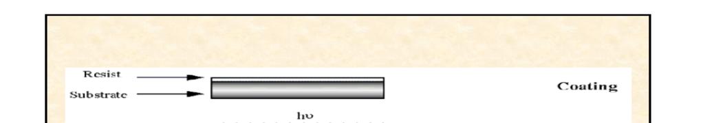
 Technische Universität Graz Institute of Solid State Physics Lithography Peter Hadley http://www.cleanroom.byu.edu/virtual_cleanroom.parts/lithography.html http://www.cleanroom.byu.edu/su8.phtml Spin coater
EMT 251 Introduction to IC Design
 EMT 251 Introduction to IC Design (Pengantar Rekabentuk Litar Terkamir) Semester II 2011/2012 Introduction to IC design and Transistor Fundamental Some Keywords! Very-large-scale-integration (VLSI) is
5. Lithography. 1. photolithography intro: overall, clean room 2. principle 3. tools 4. pattern transfer 5. resolution 6. next-gen
 5. Lithography 1. photolithography intro: overall, clean room 2. principle 3. tools 4. pattern transfer 5. resolution 6. next-gen References: Semiconductor Devices: Physics and Technology. 2 nd Ed. SM
Silicon VLSI Technology. Fundamentals, Practice and Modeling. Class Notes For Instructors. J. D. Plummer, M. D. Deal and P. B.
 Silicon VLSI Technology Fundamentals, ractice, and Modeling Class otes For Instructors J. D. lummer, M. D. Deal and. B. Griffin These notes are intended to be used for lectures based on the above text.
MAPPER: High throughput Maskless Lithography
 MAPPER: High throughput Maskless Lithography Marco Wieland CEA- Leti Alterative Lithography workshop 1 Today s agenda Introduction Applications Qualification of on-tool metrology by in-resist metrology
VLSI Design. Introduction
 Tassadaq Hussain VLSI Design Introduction Outcome of this course Problem Aims Objectives Outcomes Data Collection Theoretical Model Mathematical Model Validate Development Analysis and Observation Pseudo
+1 (479)
") Introduction to VLSI Design http://csce.uark.edu +1 (479) 575-6043 yrpeng@uark.edu Invention of the Transistor Vacuum tubes ruled in first half of 20th century Large, expensive, power-hungry, unreliable
Introduction to VLSI Design http://csce.uark.edu +1 (479) 575-6043 yrpeng@uark.edu Invention of the Transistor Vacuum tubes ruled in first half of 20th century Large, expensive, power-hungry, unreliable
Digital Integrated Circuits
 Digital Integrated Circuits Yaping Dan ( 但亚平 ), PhD Office: Law School North 301 Tel: 34206045-3011 Email: yapingd@gmail.com Digital Integrated Circuits Introduction p-n junctions and MOSFETs The CMOS
ATV 2011: Computer Engineering
 ATV 2011: Technology Trends in Computer Engineering Professor Per Larsson-Edefors ATV 2011, L1, Per Larsson-Edefors Page 1 Solid-State Devices www.cse.chalmers.se/~perla/ugrad/ SemTech/Lectures_2000.pdf
Integrated Circuit Technology (Course Code: EE662) Lecture 1: Introduction
 Lecture 1: Introduction") Indian Institute of Technology Jodhpur, Year 2015 2016 Integrated Circuit Technology (Course Code: EE662) Lecture 1: Introduction Course Instructor: Shree Prakash Tiwari, Ph.D. Email: sptiwari@iitj.ac.in
Indian Institute of Technology Jodhpur, Year 2015 2016 Integrated Circuit Technology (Course Code: EE662) Lecture 1: Introduction Course Instructor: Shree Prakash Tiwari, Ph.D. Email: sptiwari@iitj.ac.in
Mask Technology Development in Extreme-Ultraviolet Lithography
 Mask Technology Development in Extreme-Ultraviolet Lithography Anthony Yen September 6, 2013 Projected End of Optical Lithography 2013 TSMC, Ltd 1976 1979 1982 1985 1988 1991 1994 1997 2000 2003 2007 2012
EUV lithography: status, future requirements and challenges
 EUV lithography: status, future requirements and challenges EUVL Dublin Vadim Banine with the help of Rudy Peters, David Brandt, Igor Fomenkov, Maarten van Kampen, Andrei Yakunin, Vladimir Ivanov and many
ASML Market dynamics. Dave Chavoustie EVP Sales Analyst Day, September 30, 2004
 ASML Market dynamics Dave Chavoustie EVP Sales Analyst Day, September 30, 2004 Agenda! Market Overview! Growth Opportunities! 300mm Market! Asia Overview / Slide 2 ASML Unit Market Share Trend 60% 12 &
From ArF Immersion to EUV Lithography
 From ArF Immersion to EUV Lithography Luc Van den hove Vice President IMEC Outline Introduction 193nm immersion lithography EUV lithography Global collaboration Conclusions Lithography is enabling 1000
IC Knowledge LLC, PO Box 20, Georgetown, MA Ph: (978) , Fx: (978)
 , Fx: (978)") IC Knowledge LLC, PO Box 20, Georgetown, MA 01833 www.icknowledge.com Ph: (978) 352 7610, Fx: (978) 352 3870 Linx Consulting, PO Box 384, Mendon, MA 01756 0384 www.linxconsulting.com Ph: (617) 273 8837
IC Knowledge LLC, PO Box 20, Georgetown, MA 01833 www.icknowledge.com Ph: (978) 352 7610, Fx: (978) 352 3870 Linx Consulting, PO Box 384, Mendon, MA 01756 0384 www.linxconsulting.com Ph: (617) 273 8837
Intel Technology Journal
 Volume 06 Issue 02 Published, May 16, 2002 ISSN 1535766X Intel Technology Journal Semiconductor Technology and Manufacturing The Intel Lithography Roadmap A compiled version of all papers from this issue
Enabling Breakthroughs In Technology
 Enabling Breakthroughs In Technology Mike Mayberry Director of Components Research VP, Technology and Manufacturing Group Intel Corporation June 2011 Defined To be defined Enabling a Steady Technology
Enabling Semiconductor Innovation and Growth
 Enabling Semiconductor Innovation and Growth EUV lithography drives Moore s law well into the next decade BAML 2018 APAC TMT Conference Taipei, Taiwan Craig De Young Vice President IR - Asia IR March 14,
Application-Based Opportunities for Reused Fab Lines
 Application-Based Opportunities for Reused Fab Lines Semicon China, March 17 th 2010 Keith Best Simax Lithography S I M A X A L L I A N C E P A R T N E R S Outline Market: Exciting More than Moore applications
Section 2: Lithography. Jaeger Chapter 2 Litho Reader. EE143 Ali Javey Slide 5-1
 Section 2: Lithography Jaeger Chapter 2 Litho Reader EE143 Ali Javey Slide 5-1 The lithographic process EE143 Ali Javey Slide 5-2 Photolithographic Process (a) (b) (c) (d) (e) (f) (g) Substrate covered
Introduction to Materials Engineering: Materials Driving the Electronics Revolution Robert Hull, MSE
 Introduction to Materials Engineering: Materials Driving the Electronics Revolution Robert Hull, MSE Outline Microelectronics Miniaturization Historical Development: Electronics before Semiconductors The
Discovering Electrical & Computer Engineering. Carmen S. Menoni Professor Week 3 armain.
 Discovering Electrical & Computer Engineering Carmen S. Menoni Professor Week 3 http://www.engr.colostate.edu/ece103/semin armain.html TOP TECH 2012 SPECIAL REPORT IEEE SPECTRUM PAGE 28, JANUARY 2012 P.E.
Introduction to VLSI ASIC Design and Technology
 Introduction to VLSI ASIC Design and Technology Paulo Moreira CERN - Geneva, Switzerland Paulo Moreira Introduction 1 Outline Introduction Is there a limit? Transistors CMOS building blocks Parasitics
R&D Status and Key Technical and Implementation Challenges for EUV HVM
 R&D Status and Key Technical and Implementation Challenges for EUV HVM Sam Intel Corporation Agenda Requirements by Process Node EUV Technology Status and Gaps Photoresists Tools Reticles Summary 2 Moore
GIGAPHOTON INTRODUCTION
 GIGAPHOTON INTRODUCTION 15 th September 2017 Tatsuo Enami Director and Senior Executive Officer GIGAPHOTON Copyright Gigaphoton Inc. Outline of Gigaphoton Business Light source business
immersion optics Immersion Lithography with ASML HydroLith TWINSCAN System Modifications for Immersion Lithography by Bob Streefkerk
 immersion optics Immersion Lithography with ASML HydroLith by Bob Streefkerk For more than 25 years, many in the semiconductor industry have predicted the end of optical lithography. Recent developments,
New Process Technologies Will silicon CMOS carry us to the end of the Roadmap?
 HPEC Workshop 2006 New Process Technologies Will silicon CMOS carry us to the end of the Roadmap? Craig L. Keast, Chenson Chen, Mike Fritze, Jakub Kedzierski, Dave Shaver HPEC 2006-1 Outline A brief history
UV Nanoimprint Stepper Technology: Status and Roadmap. S.V. Sreenivasan Sematech Litho Forum May 14 th, 2008
 UV Nanoimprint Stepper Technology: Status and Roadmap S.V. Sreenivasan Sematech Litho Forum May 14 th, 2008 Overview Introduction Stepper technology status: Patterning and CD Control Through Etch Alignment
Legacy & Leading Edge Both are Winners
 Legacy & Leading Edge Both are Winners Semicon CMP User Group July 16, 2015 Sue Davis 408-833-5905 CMP Team Contributors: Mike Fury, Ph.D. Karey Holland, Ph.D. Jerry Yang, Ph.D. www.techcet.com 1 Outline
Section 2: Lithography. Jaeger Chapter 2 Litho Reader. The lithographic process
 Section 2: Lithography Jaeger Chapter 2 Litho Reader The lithographic process Photolithographic Process (a) (b) (c) (d) (e) (f) (g) Substrate covered with silicon dioxide barrier layer Positive photoresist
Photolithography Technology and Application
 Photolithography Technology and Application Jeff Tsai Director, Graduate Institute of Electro-Optical Engineering Tatung University Art or Science? Lind width = 100 to 5 micron meter!! Resolution = ~ 3
Lithography in our Connected World
 Lithography in our Connected World SEMI Austin Spring Forum TOP PAN P R INTING CO., LTD MATER IAL SOLUTIONS DIVISION Toppan Printing Co., LTD A Broad-Based Global Printing Company Foundation: January 17,
2008 European EUVL. EUV activities the EUVL shop future plans. Rob Hartman
 2008 European EUVL EUV activities the EUVL shop future plans Rob Hartman 2007 international EUVL Symposium 28-31 October 2007 2008 international EUVL Symposium 28 Sapporo, September Japan 1 October 2008
Transistor Scaling in the Innovation Era. Mark Bohr Intel Senior Fellow Logic Technology Development August 15, 2011
 Transistor Scaling in the Innovation Era Mark Bohr Intel Senior Fellow Logic Technology Development August 15, 2011 MOSFET Scaling Device or Circuit Parameter Scaling Factor Device dimension tox, L, W
ISSCC 2003 / SESSION 1 / PLENARY / 1.1
 ISSCC 2003 / SESSION 1 / PLENARY / 1.1 1.1 No Exponential is Forever: But Forever Can Be Delayed! Gordon E. Moore Intel Corporation Over the last fifty years, the solid-state-circuits industry has grown
Outline. Introduction on IMEC & IMEC cooperation model. Program Challenges in CMOS scaling
 imec 2009 1 The Role of European Research Institutes in the 450mm Wafer Transition Process IMEC nanoelectronics platform A Collaborative approach towards 450mm R&D IMEC March 2009 Outline Introduction
Advanced Digital Integrated Circuits. Lecture 2: Scaling Trends. Announcements. No office hour next Monday. Extra office hour Tuesday 2-3pm
 EE241 - Spring 20 Advanced Digital Integrated Circuits Lecture 2: Scaling Trends and Features of Modern Technologies Announcements No office hour next Monday Extra office hour Tuesday 2-3pm 2 1 Outline
Introduction. Digital Integrated Circuits A Design Perspective. Jan M. Rabaey Anantha Chandrakasan Borivoje Nikolic. July 30, 2002
 Digital Integrated Circuits A Design Perspective Jan M. Rabaey Anantha Chandrakasan Borivoje Nikolic Introduction July 30, 2002 1 What is this book all about? Introduction to digital integrated circuits.
Lecture 0: Introduction
 Lecture 0: Introduction Introduction Integrated circuits: many transistors on one chip. Very Large Scale Integration (VLSI): bucketloads! Complementary Metal Oxide Semiconductor Fast, cheap, low power
Update on 193nm immersion exposure tool
 Update on 193nm immersion exposure tool S. Owa, H. Nagasaka, Y. Ishii Nikon Corporation O. Hirakawa and T. Yamamoto Tokyo Electron Kyushu Ltd. January 28, 2004 Litho Forum 1 What is immersion lithography?
Part 5-1: Lithography
 Part 5-1: Lithography Yao-Joe Yang 1 Pattern Transfer (Patterning) Types of lithography systems: Optical X-ray electron beam writer (non-traditional, no masks) Two-dimensional pattern transfer: limited
Semiconductor Manufacturing Technology. Semiconductor Manufacturing Technology. Photolithography: Resist Development and Advanced Lithography
 Semiconductor Manufacturing Technology Michael Quirk & Julian Serda October 2001 by Prentice Hall Chapter 15 Photolithography: Resist Development and Advanced Lithography Eight Basic Steps of Photolithography
Lecture 7. Lithography and Pattern Transfer. Reading: Chapter 7
 Lecture 7 Lithography and Pattern Transfer Reading: Chapter 7 Used for Pattern transfer into oxides, metals, semiconductors. 3 types of Photoresists (PR): Lithography and Photoresists 1.) Positive: PR
Optical Microlithography XXVIII
 PROCEEDINGS OF SPIE Optical Microlithography XXVIII Kafai Lai Andreas Erdmann Editors 24-26 February 2015 San Jose, California, United States Sponsored by SPIE Cosponsored by Cymer, an ASML company (United
Feature-level Compensation & Control
 Feature-level Compensation & Control 2 Sensors and Control Nathan Cheung, Kameshwar Poolla, Costas Spanos Workshop 11/19/2003 3 Metrology, Control, and Integration Nathan Cheung, UCB SOI Wafers Multi wavelength
Roadmap Semiconductor Equipment Innovation Agenda
 Roadmap Semiconductor Equipment Innovation Agenda 2018-2021 1. Societal and economic relevance Over the years, electronics have become an inseparable part of our lives. Think of the internet, the cloud,
Lithography Roadmap. without immersion lithography. Node Half pitch. 248nm. 193nm. 157nm EUVL. 3-year cycle: 2-year cycle: imec 2005
 Lithography Roadmap without immersion lithography Node Half pitch 180 nm 130 nm 90 nm 65 nm 45 nm 32 nm 22 nm 250 nm 180 nm 130 nm 90 nm 65 nm 45 nm 32 nm 248nm 193nm 157nm EUVL 3-year cycle: 2-year cycle:
Development Status of EUV Sources for Use in Alpha-, Beta- and High Volume Chip Manufacturing Tools
 Development Status of EUV Sources for Use in Alpha-, Beta- and High Volume Chip Manufacturing Tools Uwe Stamm, Jürgen Kleinschmidt, Bernd Nikolaus, Guido Schriever, Max Christian Schürmann, Christian Ziener
Plan Optik AG. Plan Optik AG PRODUCT CATALOGUE
 Plan Optik AG Plan Optik AG PRODUCT CATALOGUE 2 In order to service the high demand of wafers more quickly, Plan Optik provides off the shelf products in sizes from 2 up to 300mm diameter. Therefore Plan
The SEMATECH Model: Potential Applications to PV
 Continually cited as the model for a successful industry/government consortium Accelerating the next technology revolution The SEMATECH Model: Potential Applications to PV Dr. Michael R. Polcari President
Limitations and Challenges to Meet Moore's Law
 Limitations and Challenges to Meet Moore's Law Sept 10, 2015 Sung Kim sung_kim@amat.com State of the art: cleanroom toolsets metrology analysis module development test & reliability Introduction Why do
Holst Centre Wireless Autonomous Sensor Technologies & Flexible Electronics
 February 10, 2011 Holst Centre Wireless Autonomous Sensor Technologies & Flexible Electronics Presentation overview -General overview -Research focus < 4 Holst Centre: a solid partner in research Independent,
Technology for the MEMS processing and testing environment. SUSS MicroTec AG Dr. Hans-Georg Kapitza
 Technology for the MEMS processing and testing environment SUSS MicroTec AG Dr. Hans-Georg Kapitza 1 SUSS MicroTec Industrial Group Founded 1949 as Karl Süss KG GmbH&Co. in Garching/ Munich San Jose Waterbury
Status and challenges of EUV Lithography
 Status and challenges of EUV Lithography SEMICON Europa Dresden, Germany Jan-Willem van der Horst Product Manager EUV October 10 th, 2013 Slide 2 Contents Introduction NXE:3100 NXE:3300B Summary and acknowledgements
EE4800 CMOS Digital IC Design & Analysis. Lecture 1 Introduction Zhuo Feng
 EE4800 CMOS Digital IC Design & Analysis Lecture 1 Introduction Zhuo Feng 1.1 Prof. Zhuo Feng Office: EERC 730 Phone: 487-3116 Email: zhuofeng@mtu.edu Class Website http://www.ece.mtu.edu/~zhuofeng/ee4800fall2010.html
Imec pushes the limits of EUV lithography single exposure for future logic and memory
 Edition March 2018 Semiconductor technology & processing Imec pushes the limits of EUV lithography single exposure for future logic and memory Imec has made considerable progress towards enabling extreme
Sub-micron technology IC fabrication process trends SOI technology. Development of CMOS technology. Technology problems due to scaling
 Goodbye Microelectronics Welcome Nanoelectronics Sub-micron technology IC fabrication process trends SOI technology SiGe Tranzistor in 50nm process Virus The thickness of gate oxide= 1.2 nm!!! Today we
research in the fields of nanoelectronics
 FRAUNHOFEr center Nanoelectronic Technologies research in the fields of nanoelectronics 1 contents Fraunhofer CNT in Profile 3 Competence Areas Analytics 4 Functional Electronic Materials 5 Device & Integration
Section 2: Lithography. Jaeger Chapter 2. EE143 Ali Javey Slide 5-1
 Section 2: Lithography Jaeger Chapter 2 EE143 Ali Javey Slide 5-1 The lithographic process EE143 Ali Javey Slide 5-2 Photolithographic Process (a) (b) (c) (d) (e) (f) (g) Substrate covered with silicon
Noel Technologies. Provider of Advanced Lithography and Semiconductor Thin Film Services
 Noel Technologies Provider of Advanced Lithography and Semiconductor Thin Film Services Noel Technologies Keith Best Biography Over the last 27 years, Keith Best has held a variety of semiconductor processing
IMI Labs Semiconductor Applications. June 20, 2016
 IMI Labs Semiconductor Applications June 20, 2016 Materials Are At the Core of Innovation in the 21st Century Weight Space Flexibility Heat Management Lightweight Energy Efficient Temperature Energy Efficient
Reliable High Power EUV Source Technology for HVM: LPP or DPP? Vivek Bakshi, Ph.D. EUV Litho, Inc.
 Reliable High Power EUV Source Technology for HVM: LPP or DPP? Vivek Bakshi, Ph.D. EUV Litho, Inc. Presentation Outline Source Technology Requirements Source Technology Performance DPP LPP Technology Trend
Used Semiconductor Manufacturing Equipment: Looking for Sales in All the Right Places. Study Number MA108-09
 Study Number MA108-09 August 2009 Copyright Semico Research, 2009. All rights reserved. Reproduction in whole or part is prohibited without permission of Semico. The contents of this report represent
Triple i - The key to your success
 Triple i - The key to your success The needs and challenges of today s world are becoming ever more demanding. Standards are constantly rising. Creativity, reliability and high performance are basic prerequisites