ASCENT. European Nanoelectronics Infrastructure Access. Nicolás Cordero
|
|
|
- Cecilia Walton
- 6 years ago
- Views:
Transcription


1 ASCENT European Nanoelectronics Infrastructure Access Nicolás Cordero


2 The Challenge Cost/performance returns by scaling are diminishing Cost to achieve tape out on new nodes is increasing Technology Quarterly March 12, 2016

3 The infrastructure A truly unique opportunity: ASCENT combines Tyndall, imec and CEA-Leti s nanofabrication & electrical characterisation capabilities into a single research infrastructure and makes it accessible to all
4 Objectives ASCENT will: Leverage Europe s Unique advantage in nanofabrication to strengthen modeling and characterisation research community Accelerate development of advanced models at scales of 14nm and below Provide characterisation community with access to advanced test chips, flexible fabrication and advanced test and characterisation equipment Make project outputs available and easily accessible to nanoelectronics research community ASCENT offers simplified access to advanced technology and research infrastructure

5 ASCENT Network

6 >220 members of ASCENT Network
7 Committee Membership Industry Innovation Committee Bernie Capraro Intel Patrick Drennan Qualcomm Ronald Gull Synopsys Dominique Thomas ST Microelectronics Users Committee George Angelov TU Sofia Asen Asenov Uni Glasgow Francisco Gamiz Uni Granada Benjamin Iñiguez Uni Rovira i Virgili Andreas Schenk ETH


8 Access Provided State-of-the-art 14 nm bulk FDSOI CMOS Advanced transistor and interconnect test structures Fabrication facilities for nanowires & 2D materials Advanced nanowire and nano- electrode test structures State-of-the-art 14 nm FinFET CMOS Advanced transistor and interconnect test structures Electrical & nanocharacterization platforms Electrical & nanocharacterization platforms Electrical & nanocharacterisation platforms
9 Access Provided Test wafer/chips Electrical Characterisation Physical Characterisation Nanoscale non-standard fabrication 14nm technology data (Virtual Access)


10 FinFET 14/28nm Material for Device Analysis Test chips/wafers 300mm wafers with Bulk FinFET devices (14nm) 300mm wafers with Planar Metal Gate devices (28nm) Digital and Analog/RF existing test chips Complete suite of test structures for Reliability/ESD/Matching/Local Layout effects/... Standard devices up to circuit level [Ring-Oscillators,...] State-of-the-art bulk FinFET device baseline

 To come in the near future: Spice model for Stacked NWs (7nm")
11 FDSOI 14/28nm Material for Device Analysis 300mm wafers with planar FDSOI and Nanowire devices SPICE models and model cards for digital: target and preliminary 14nm FDSOI 10nm FDSOI 10nm FFSOI TCAD decks FDSOI MOSFET Trigate SOI Nanowire GAA Nanowire MOSFET (mainly electrostatics) To come in the near future: Spice model for Stacked NWs (7nm tech. node)


 on 300mm prober Electrostatic discharge")
12 Electrical Characterisation >500 m 2 of test labs, ~ 25 semiauto/manual 300mm probers Statistical data treatment in JMP Fully and Semi-automatic 300mm parametric testers Temperature range for test on wafers 77/10K high T Fast Pulse testing, Self-Heating characterization HF tests up to 50 GHz Noise measurements Reliability tests: hot carriers, TDDB, charge pumping, High power tests (10kV, > 100A) on 300mm prober Electrostatic discharge LAB
-C(V) 200/300mm testers Temperature range for test on wafers: 2K 600 C Test systems for memories HF tests up to 40 MHz Noise")
 on 300mm prober Deep Level Transient Spectroscopy Electrostatic discharges Electromigration Oven and")
13 Electrical Characterisation Parametric testers with 300mm full auto probers Probe cards and new membrane cards Statistical data treatment Functional tests General purpose I(V)-C(V) 200/300mm testers Temperature range for test on wafers: 2K 600 C Test systems for memories HF tests up to 40 MHz Noise measurements Reliability tests: hot carriers, TDDB, charge pumping, Internal Photo Emission Emission microscopy (visible & infrared) Electrical test under calibrated strain High power tests (10kV, > 100A) on 300mm prober Deep Level Transient Spectroscopy Electrostatic discharges Electromigration Oven and climatic environments


14 Electrical Characterisation Labs Open Access Test Lab Nanoscale Test Lab Reliability Test Lab Wide range of test equipment for device and wafer testing e.g.: impedance, capacitance, voltage, current, spectrum analysers, Variable Temperature, Micromanipulator Probe Stations Wide range of test equipment for packaged devices

 Spectrometer/microscope PHI VERSA PROBE II Ellipsometer Ultraviolet-visible ellipsometer - HORIBA")
15 Physical Characterisation Atomic Force Microscopy Dimension AFM Icon/Fast Scan Bruker working under glovebox (O2, H2O < 1 ppm) High Resolution Transmission Electron Microscopy FEI TECNAI G2 F 20 FEI TITAN THEMIS kv ToF-SIMS ION TOF ToF SIMS 5 Atom Probe Tomography CAMECA FlexTAP Atom probe XRD (X-ray Diffraction) Diffractometer Smartlab RIGAKU 5 circles XPS (X-ray Photoelectron Spectroscopy) Spectrometer/microscope PHI VERSA PROBE II Ellipsometer Ultraviolet-visible ellipsometer - HORIBA JOBIN YVON UVISEL


16 Physical Characterisation Labs Electron Microscopy Facility Nanoscale Characterisation Optical Spectroscopy Labs Magnetic Characterisation Package Characterisation High Resolution TEM, SEM and FIB, EDAX capability AFM, SEM and electrical characterisation Raman & Optical Spectroscopy, fluorescence microscopy SQUID magnetometer for nano magnetic materials Scanning Acoustic microscope, X-ray analysis


17 Nanoscale fabrication Range of cleanrooms designed for flexible process & product development Silicon MOS Fabrication MEMS Fabrication Compound Semiconductor Fabrication Photonics Fab Training Facility e-beam Lithography Non-standard nano-processing


 Oxford Instruments X-MAX 80 for high productivity EDS analysis JEOL")
18 Focussed Ion Beam (FIB) Complete nanotechnology lab in one tool High resolution pole piece point-topoint resolution of 0.21 nm EDS, Oxford instruments, INCA 250, site-lock drift correction system for high resolution elemental mapping In-situ STM-TEM holders, high temperature TEM holders STEM mode with BF and HAADF detectors (0.8 nm resolution) Oxford Instruments X-MAX 80 for high productivity EDS analysis JEOL 2100 HR-(S)TEM / FEI Helios NanoLab DB-FIB Cryo preparation for liquid and gellike materials
19 Nanoscale Technology Data (Virtual Access) FinFET and GAA test chip documentation and DATA (14nm) Documentation of process assumptions for the test chips Inventory of test structure types available on the test chips Access to test structures data III/V InGaAs GAA test chip documentation and DATA Documentation of process assumptions for the test chips Inventory of test structure types available on the test chips Access to test structures data PLANAR test chip documentation and DATA (28nm) Documentation of process assumptions for the test chips Inventory of test structure types available on the test chips Access to test structures data FDSOI: PDK for Full custom IC design 14nm planar FDSOI technology 10nm planar FDSOI technology (preliminary)

20 Virtual Access Data available


21 imec bulk FinFET data Access to bulk finfet and GAA_SiNW data Integrated dual WFM CMOS LG range 24nm 90nm within pitch and long channel devices nfin from 2 to 22 Room T available 50 C or higher T next Low T can be considered DOE for contact, layout effects,...
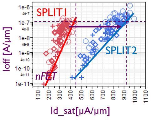
![ID[A] ID[A] imec bulk FinFET data Access to raw data and extracted FoM s Threshold](/docs-images/78/77410822/images/22-2.jpg "Voltage, Mismatch DC metrics and ID-VD, ID-VG characteristics FEOL/BEOL R/C and")

22 ID[A] ID[A] imec bulk FinFET data Access to raw data and extracted FoM s Threshold Voltage, Mismatch DC metrics and ID-VD, ID-VG characteristics FEOL/BEOL R/C and Ring-Oscillator circuits Full sweep data in VA Covers range of VG/VD and LG/nFin VG[V] Analog FoM, Reliability testing, ESD,... Available for subsequent model validation VG[V] VD[V]
 with possible back-biasing up to Vdd DRM: simplified design rules BEOL MEOL FEOL Design Kit FDSOI")
23 PROCESS ASSUMPTIONS PLANAR 14NM FDSOI TECHNOLOGY FOR BENCHMARKING CPP = 90nm Nominal supply voltage Vdd=1V BEOL: Metal levels: Metal 1 to Metal 5, Pitch = 64nm (similar to 20nm bulk) MEOL: Trench contact Metal0 FEOL: FDSOI transistor with Lmin = 20nm Standard Well definition (similar to bulk) with possible back-biasing up to Vdd DRM: simplified design rules BEOL MEOL FEOL Design Kit FDSOI 14nm CIBRARIO Gérald
 RC Simulation Technology")

 Layout Parameterized")

24 FULL CUSTOM DESIGN FLOW Parasitic extraction (PEX) RC Simulation Technology Devices Library: N/P FET (multi-vt) Spice Modeling NFET Post-Layout Simulation DRM, Reference manuals Design Library Simulation Verification (DRC/LVS) Layout Parameterized cells (MOS Pcells) Design Rules Checking Extraction Devices Design Kit FDSOI 14nm CIBRARIO Gérald
 - SPICE Model: library of MOSFET devices (UTSOI2)")
 - Pcell: library of parameterized MOSFET for layout automation")
: comparison layout vs simulation -")
: netlist simulation with RC elements -")
 analysis, architecture definition (template) Design Kit FDSOI 14nm")
25 PDK FDSOI 14NM CONTENTS - Electrical simulation for design performance (Schematic Netlist) - SPICE Model: library of MOSFET devices (UTSOI2) integrated - Layout: physical implementation of all technological layers (Techfile) - Pcell: library of parameterized MOSFET for layout automation - Design Rules Check (DRC): deck file describing all design rules (DRM) - Layout Versus Schematic (LVS): comparison layout vs simulation - Parasitic EXtraction (PEX): extraction of parasitic elements (RC) - Post-Layout Simulation (PLS): netlist simulation with RC elements - Digital Library: preliminary basic logic cells for Power Performance Area (PPA) analysis, architecture definition (template) Design Kit FDSOI 14nm CIBRARIO Gérald
26 TECHNOLOGICAL LIBRARY LIBRARY NAME: DK_FDSOI14LIB Library Technological file include technology, layer information, display and layer map files, Based on the OpenAccess Database Symbol Pcell Symbol library contains 8 variants of device symbols for MOS => 8 n/p fet (SVT1/SVT2/LVT/HVT), Associated SPICE models for simulation MOS parameterized cells available to reduce layout time and design rule mistakes, Pcells manage all kinds of MOS devices and all VT options LVTNFET Parameters: l : 20nm w : 46nm nf : 1 m : 1 Design Kit FDSOI 14nm CIBRARIO Gérald

 Stressor effects: Continuous RX, Isolated MOS Pre-layout effects: R, C, R+C Design Kit FDSOI")
27 FEOL SPICE MODELS (1/2) SPICE MODEL FOR FDSOI: UTSOI2 The UTSOI2 compact model was developed to describe the electrical behavior of FDSOI transistor: especially back biasing effect Several versions are available in major IC simulators (Eldo, Spectre, Hspice, ADS,...) The FDSOI MOSFET is a 4 pins device as bulk Bulk (B) FDSOI MOSFET is symmetric: drain source: no junction as in bulk Well Included in device library: Parasitic effects: Area SD region (AS-AD) Stressor effects: Continuous RX, Isolated MOS Pre-layout effects: R, C, R+C Design Kit FDSOI 14nm CIBRARIO Gérald

28 FEOL SPICE MODELS (2/2) MULTI-VT DESCRIPTION FOR BENCHMARKING VT definition in PDK: several gate workfunctions VT Description Well for nfet Well for pfet LVT Low-VT N P SVT1 Standard-VT1 N P SVT2 Standard-VT2 P N HVT High-VT P N Multi-VT platform can be managed using several solutions: Poly-biasing: Lnom + x nm Back-biasing: for example +Vdd under nfet Gate workfunctions Multi-VT strategy is foundry-dependent Design Kit FDSOI 14nm CIBRARIO Gérald
.")
29 PHYSICAL IMPLEMENTATION LAYOUT STRATEGY Continuous RX: used for increasing devices performance Poly pitch: value is 90nm Special Construct: used for MEOL layers in dedicated areas. To highlight special construct, used the associated marker (MKR_ SpeConst). This allows to waive a set of default rules and check some other specific design rules (see DRM for more details) MKR_GateTie: this marker must be placed on poly regions. These gates are formed each time we want to abut 2 devices which don t share the same active regions. The device we are getting is a transistor in OFF state called gate tie. With this marker, the LVS will be able to extract this device Design Kit FDSOI 14nm CIBRARIO Gérald


30 PHYSICAL VERIFICATION PLATFORM Design Rules Checking (DRC) DRC deck file manage: One-Dimensional check, Multi-Dimensional check, Interdependent Multi-Layer check Layout Versus Schematic (LVS) Y X Y X (x/x) 2 + (y/y) 2 = 1 Gate direction MOS devices extraction: VT option & Gate Tie device Well-tie for Back-gate control MOS parameters extraction: Geometry: l/w/nf/m Area: as/ad/ps/pd Stressor effects: sa/sb/sd Connectivity declaration Design Kit FDSOI 14nm CIBRARIO Gérald
 2 descriptions: StarRC")
 Description of the FDSOI cross-section:")

31 PARASITIC EXTRACTION FLOW (PEX) POST-LAYOUT SIMULATION: Parasitic extraction files: Technological and mapping files, Nominal (corners not available) 2 descriptions: StarRC / xcalibrate, Ignore FEOL capacitances (SPICE) Metal resistance included IGNORE_CAPACITANCE (embedded in SPICE model) Description of the FDSOI cross-section: DIELECTRIC / CONDUCTOR / VIA Technological information: THICKNESS / PERMITTIVITY / RESISTIVITY Output: netlist including RC parasitic elements for PLS Design Kit FDSOI 14nm CIBRARIO Gérald
 release 2015.1_14.11 PEX Star-RC (Synopsys) release 2012.12-SP2 Calibre (Mentor) release 2015.2.19.")
32 CAD TOOLS RECOMMENDATION Flow CAD tools & releases Framework Virtuoso(Cadence) release IC Simulator Eldo (Mentor) release 13_2c HSPICE (Synopsys) release SP2 DRC/LVS Calibre (Mentor) release _14.11 PEX Star-RC (Synopsys) release SP2 Calibre (Mentor) release Design Kit FDSOI 14nm CIBRARIO Gérald
 UK 031 X. Wang Univ. Glasgow UK 035 K. Miyaguchi IMEC Belgium 036 G.")

33 Virtual Access Users Ref User Institute Country 002 G. Angelov T.U. Sofia Bulgaria 006 G. Fatin Univ. Maynooth Ireland 008 A. Durgaryan Synopsys Armenia 022 A. Nejadmalayeri Phoelex Ltd (SME) UK 031 X. Wang Univ. Glasgow UK 035 K. Miyaguchi IMEC Belgium 036 G. Ghibaudo IMEP-LAHC/INPG France 037 F. Gamiz Univ. Granada Spain 043 M. Karner GlobalTCAD Solutions GmbH Austria 045 T. Kelly EOLAS Designs Ireland 047 A. Pezzotta EPFL ICLAB Switzerland 057 C. Couso Univ. Aut. Barcelona Spain 058 M. Bucher T.U. Crete Greece 062 L. Dobrescu T.U. Bucharest Romania 2


34 Next step Please join us in this exciting opportunity for nanoelectronics research Sign up: Phone: Sign up and find out more online OR Fill out a card and we ll sign you up
ASCENT Overview. European Nanoelectronics Infrastructure Access. MOS-AK Workshop, Infineon, Munich, 13 th March 2018.
 ASCENT Overview MOS-AK Workshop, Infineon, Munich, 13 th March 2018 European Nanoelectronics Infrastructure Access Paul Roseingrave The Challenge Cost/performance returns by scaling are diminishing Cost
ASCENT Open Access to 14nm PDKs T. Chiarella, N. Cordero, O. Faynot on behalf of the ASCENT teams
 ASCENT Open Access to 14nm PDKs T. Chiarella, N. Cordero, O. Faynot on behalf of the ASCENT teams chiarel@imec.be 11/09/2017 MOS AK Workshop @ ESSDERC 2017 Leuven, BE Content ASCENT in a nutshell Individual
Advanced PDK and Technologies accessible through ASCENT
 Advanced PDK and Technologies accessible through ASCENT MOS-AK Dresden, Sept. 3, 2018 L. Perniola*, O. Rozeau*, O. Faynot*, T. Poiroux*, P. Roseingrave^ olivier.faynot@cea.fr *Cea-Leti, Grenoble France;
Deliverable 4.2: TEM cross sections on prototyped Gated Resistors
 Deliverable 4.2: TEM cross sections on prototyped Gated Resistors Olga G. Varona, Geoff Walsh, Bernie Capraro Intel Ireland 21 June 2011 Abbreviation list D: drain FIB: focused ion-beam HRTEM: high resolution
45nm Foundry CMOS with Mask-Lite Reduced Mask Costs
 This work is sponsored by the Air Force Research Laboratory (AFRL/RVSE) TPOC: Mr. Kenneth Hebert 45nm Foundry CMOS with Mask-Lite Reduced Mask Costs 25 October 2011 www.americansemi.com 2011 American Semiconductor,
DATASHEET CADENCE QRC EXTRACTION
 DATASHEET Cadence QRC Etraction, the industry s premier 3D fullchip parasitic etractor that is independent of design style or flow, is a fast and accurate RLCK etraction solution used during design implementation
EUROSOI+- FP of 38 30/06/ FINAL PUBLISHABLE SUMMARY REPORT
 EUROSOI+- FP7-216373 3 of 38 30/06/2011 1. FINAL PUBLISHABLE SUMMARY REPORT EUROSOI+- FP7-216373 4 of 38 30/06/2011 EUROSOI+- FP7-216373 5 of 38 30/06/2011 The main and last objective of EUROSOI Network
ECE 5745 Complex Digital ASIC Design Topic 2: CMOS Devices
 ECE 5745 Complex Digital ASIC Design Topic 2: CMOS Devices Christopher Batten School of Electrical and Computer Engineering Cornell University http://www.csl.cornell.edu/courses/ece5950 Simple Transistor
write-nanocircuits Direct-write Jaebum Joo and Joseph M. Jacobson Molecular Machines, Media Lab Massachusetts Institute of Technology, Cambridge, MA
 Fab-in in-a-box: Direct-write write-nanocircuits Jaebum Joo and Joseph M. Jacobson Massachusetts Institute of Technology, Cambridge, MA April 17, 2008 Avogadro Scale Computing / 1 Avogadro number s? Intel
research in the fields of nanoelectronics
 FRAUNHOFEr center Nanoelectronic Technologies research in the fields of nanoelectronics 1 contents Fraunhofer CNT in Profile 3 Competence Areas Analytics 4 Functional Electronic Materials 5 Device & Integration
450mm and Moore s Law Advanced Packaging Challenges and the Impact of 3D
 450mm and Moore s Law Advanced Packaging Challenges and the Impact of 3D Doug Anberg VP, Technical Marketing Ultratech SOKUDO Lithography Breakfast Forum July 10, 2013 Agenda Next Generation Technology
Jack Keil Wolf Lecture. ESE 570: Digital Integrated Circuits and VLSI Fundamentals. Lecture Outline. MOSFET N-Type, P-Type.
 ESE 570: Digital Integrated Circuits and VLSI Fundamentals Jack Keil Wolf Lecture Lec 3: January 24, 2019 MOS Fabrication pt. 2: Design Rules and Layout http://www.ese.upenn.edu/about-ese/events/wolf.php
Bridging the Gap between Dreams and Nano-Scale Reality
 Bridging the Gap between Dreams and Nano-Scale Reality Ban P. Wong Design Methodology, Chartered Semiconductor wongb@charteredsemi.com 28 July 2006 Outline Deficiencies in Boolean-based Design Rules in
Fin-Shaped Field Effect Transistor (FinFET) Min Ku Kim 03/07/2018
 Min Ku Kim 03/07/2018") Fin-Shaped Field Effect Transistor (FinFET) Min Ku Kim 03/07/2018 ECE 658 Sp 2018 Semiconductor Materials and Device Characterizations OUTLINE Background FinFET Future Roadmap Keeping up w/ Moore s Law
Fin-Shaped Field Effect Transistor (FinFET) Min Ku Kim 03/07/2018 ECE 658 Sp 2018 Semiconductor Materials and Device Characterizations OUTLINE Background FinFET Future Roadmap Keeping up w/ Moore s Law
FD-SOI FOR RF IC DESIGN. SITRI LETI Workshop Mercier Eric 08 september 2016
 FD-SOI FOR RF IC DESIGN SITRI LETI Workshop Mercier Eric 08 september 2016 UTBB 28 nm FD-SOI : RF DIRECT BENEFITS (1/2) 3 back-end options available Routing possible on the AluCap level no restriction
Hot Topics and Cool Ideas in Scaled CMOS Analog Design
 Engineering Insights 2006 Hot Topics and Cool Ideas in Scaled CMOS Analog Design C. Patrick Yue ECE, UCSB October 27, 2006 Slide 1 Our Research Focus High-speed analog and RF circuits Device modeling,
ESE 570: Digital Integrated Circuits and VLSI Fundamentals
 ESE 570: Digital Integrated Circuits and VLSI Fundamentals Lec 3: January 24, 2019 MOS Fabrication pt. 2: Design Rules and Layout Penn ESE 570 Spring 2019 Khanna Jack Keil Wolf Lecture http://www.ese.upenn.edu/about-ese/events/wolf.php
INTRODUCTION TO MOS TECHNOLOGY
 INTRODUCTION TO MOS TECHNOLOGY 1. The MOS transistor The most basic element in the design of a large scale integrated circuit is the transistor. For the processes we will discuss, the type of transistor
FinFET SPICE Modeling
 FinFET SPICE Modeling Synopsys Solutions to Simulation Challenges of Advanced Technology Nodes Joddy Wang December 9, 2015 Outline SPICE Model for IC Design FinFET Modeling Challenges Solutions Summary
HOW TO CONTINUE COST SCALING. Hans Lebon
 HOW TO CONTINUE COST SCALING Hans Lebon OUTLINE Scaling & Scaling Challenges Imec Technology Roadmap Wafer size scaling : 450 mm 2 COST SCALING IMPROVED PERFORMANCE 3 GLOBAL TRAFFIC FORECAST Cloud Traffic
FinFET-based Design for Robust Nanoscale SRAM
 FinFET-based Design for Robust Nanoscale SRAM Prof. Tsu-Jae King Liu Dept. of Electrical Engineering and Computer Sciences University of California at Berkeley Acknowledgements Prof. Bora Nikoli Zheng
Low-Power VLSI. Seong-Ook Jung VLSI SYSTEM LAB, YONSEI University School of Electrical & Electronic Engineering
 Low-Power VLSI Seong-Ook Jung 2013. 5. 27. sjung@yonsei.ac.kr VLSI SYSTEM LAB, YONSEI University School of Electrical & Electronic Engineering Contents 1. Introduction 2. Power classification & Power performance
Nanotechnology, the infrastructure, and IBM s research projects
 Nanotechnology, the infrastructure, and IBM s research projects Dr. Paul Seidler Coordinator Nanotechnology Center, IBM Research - Zurich Nanotechnology is the understanding and control of matter at dimensions
Introduction of New Products
 Field Emission Electron Microscope JEM-3100F For evaluation of materials in the fields of nanoscience and nanomaterials science, TEM is required to provide resolution and analytical capabilities that can
DATE 2016 Early Reliability Modeling for Aging and Variability in Silicon System (ERMAVSS Workshop)
") March 2016 DATE 2016 Early Reliability Modeling for Aging and Variability in Silicon System (ERMAVSS Workshop) Ron Newhart Distinguished Engineer IBM Corporation March 19, 2016 1 2016 IBM Corporation Background
March 2016 DATE 2016 Early Reliability Modeling for Aging and Variability in Silicon System (ERMAVSS Workshop) Ron Newhart Distinguished Engineer IBM Corporation March 19, 2016 1 2016 IBM Corporation Background
FinFET vs. FD-SOI Key Advantages & Disadvantages
 FinFET vs. FD-SOI Key Advantages & Disadvantages Amiad Conley Technical Marketing Manager Process Diagnostics & Control, Applied Materials ChipEx-2014, Apr 2014 1 Moore s Law The number of transistors
A New Model for Thermal Channel Noise of Deep-Submicron MOSFETS and its Application in RF-CMOS Design
 IEEE JOURNAL OF SOLID-STATE CIRCUITS, VOL. 36, NO. 5, MAY 2001 831 A New Model for Thermal Channel Noise of Deep-Submicron MOSFETS and its Application in RF-CMOS Design Gerhard Knoblinger, Member, IEEE,
Design and Performance Analysis of SOI and Conventional MOSFET based CMOS Inverter
 I J E E E C International Journal of Electrical, Electronics ISSN No. (Online): 2277-2626 and Computer Engineering 3(2): 138-143(2014) Design and Performance Analysis of SOI and Conventional MOSFET based
CHAPTER 6 DIGITAL CIRCUIT DESIGN USING SINGLE ELECTRON TRANSISTOR LOGIC
 94 CHAPTER 6 DIGITAL CIRCUIT DESIGN USING SINGLE ELECTRON TRANSISTOR LOGIC 6.1 INTRODUCTION The semiconductor digital circuits began with the Resistor Diode Logic (RDL) which was smaller in size, faster
Ridgetop Group, Inc.
 Ridgetop Group, Inc. Ridgetop Group Facilities in Tucson, AZ Arizona-based firm, founded in 2000, with focus on electronics for critical applications Two divisions: Semiconductor & Precision Instruments
Progress Energy Distinguished University Professor Jay Baliga. April 11, Acknowledgements
 Progress Energy Distinguished University Professor Jay Baliga April 11, 2019 Acknowledgements 1 Outline SiC Power MOSFET Breakthroughs achieved at NCSU PRESiCE: SiC Power Device Manufacturing Technology
45nm Foundry CMOS with Mask-Lite Reduced Mask Costs
 This work is sponsored in part by the Air Force Research Laboratory (AFRL/RVSE) 45nm Foundry CMOS with Mask-Lite Reduced Mask Costs 21 March 2012 This work is sponsored in part by the National Aeronautics
High-speed logic integrated circuits with solutionprocessed self-assembled carbon nanotubes
 In the format provided by the authors and unedited. DOI: 10.1038/NNANO.2017.115 High-speed logic integrated circuits with solutionprocessed self-assembled carbon nanotubes 6 7 8 9 10 11 12 13 14 15 16
Session 3: Solid State Devices. Silicon on Insulator
 Session 3: Solid State Devices Silicon on Insulator 1 Outline A B C D E F G H I J 2 Outline Ref: Taurand Ning 3 SOI Technology SOl materials: SIMOX, BESOl, and Smart Cut SIMOX : Synthesis by IMplanted
ECE 521. Design Flow. Fall 2016 Simulation. Design Verification. Why Solve Equations on a Computer?
 Design Flow Comparison with specs Redesign Concept Implementation Design Specifications Circuit Schematic ECE 521 Layout SPICE etc. Physical definition Fall 2016 Physical verification Parasitic Extraction
An EM-aware methodology for a high-speed multi-protocol 28Gbps SerDes design with TSMC 16FFC
 An EM-aware methodology for a high-speed multi-protocol 28Gbps SerDes design with TSMC 16FFC Bud Hunter, SerDes Analog IC Design Manager, Wipro Kelly Damalou, Sr. Technical Account Manager, Helic TSMC
Wafer-scale 3D integration of silicon-on-insulator RF amplifiers
 Wafer-scale integration of silicon-on-insulator RF amplifiers The MIT Faculty has made this article openly available. Please share how this access benefits you. Your story matters. Citation As Published
End-of-line Standard Substrates For the Characterization of organic
 FRAUNHOFER INSTITUTe FoR Photonic Microsystems IPMS End-of-line Standard Substrates For the Characterization of organic semiconductor Materials Over the last few years, organic electronics have become
Christian Boit TUB Berlin University of Technology Sect. Semiconductor Devices. 1
 Semiconductor Device & Analysis Center Berlin University of Technology Christian Boit TUB Berlin University of Technology Sect. Semiconductor Devices Christian.Boit@TU-Berlin.DE 1 Semiconductor Device
Lecture 6. Technology Trends and Modeling Pitfalls: Transistors in the real world
 Lecture 6 Technology Trends and Modeling Pitfalls: Transistors in the real world Guest lecturer: Jared Zerbe Rambus Inc jared@rambus.com Copyright 2004 by Mark Horowitz Some Figures courtesy of C. Enz,
IN SITU BIASING & HEATING SOLUTIONS FOR TEM PLATFORMS
 IN SITU BIASING & HEATING SOLUTIONS FOR TEM PLATFORMS Solutions for In Situ Microscopy THE LIGHTNING SERIES LIGHTNING FEATURES Observe the real-time dynamics of materials under electrical and heating stimuli.
Sub-micron technology IC fabrication process trends SOI technology. Development of CMOS technology. Technology problems due to scaling
 Goodbye Microelectronics Welcome Nanoelectronics Sub-micron technology IC fabrication process trends SOI technology SiGe Tranzistor in 50nm process Virus The thickness of gate oxide= 1.2 nm!!! Today we
Through-silicon via based 3D IC technology: Electrostatic simulations for design methodology
 Through-silicon via based 3D IC technology: Electrostatic simulations for design methodology Maxime Rousseau, Olivier Rozeau, Gérald Cibrario, Gilles Le Carval, Marie-Anne Jaud, Patrick Leduc, Alexis Farcy,
FDSOI for Low Power System on Chip. M.HAOND STMicroelectronics, Crolles, France
 FDSOI for Low Power System on Chip M.HAOND STMicroelectronics, Crolles, France OUTLINE Introduction : Motivations for FDSOI FDSOI Presentation & Short Channel control MOS VT Construction Performance Analysis
Silicon Photonics Technology Platform To Advance The Development Of Optical Interconnects
 Silicon Photonics Technology Platform To Advance The Development Of Optical Interconnects By Mieke Van Bavel, science editor, imec, Belgium; Joris Van Campenhout, imec, Belgium; Wim Bogaerts, imec s associated
Course Outcome of M.Tech (VLSI Design)
") Course Outcome of M.Tech (VLSI Design) PVL108: Device Physics and Technology The students are able to: 1. Understand the basic physics of semiconductor devices and the basics theory of PN junction. 2.
Course Outcome of M.Tech (VLSI Design) PVL108: Device Physics and Technology The students are able to: 1. Understand the basic physics of semiconductor devices and the basics theory of PN junction. 2.
! Review: MOS IV Curves and Switch Model. ! MOS Device Layout. ! Inverter Layout. ! Gate Layout and Stick Diagrams. ! Design Rules. !
 ESE 570: Digital Integrated Circuits and VLSI Fundamentals Lec 3: January 21, 2017 MOS Fabrication pt. 2: Design Rules and Layout Lecture Outline! Review: MOS IV Curves and Switch Model! MOS Device Layout!
Project SUPERAID7: Stability Under Process Variability for Advanced Interconnects and Devices Beyond 7nm node
 Project SUPERAID7: Stability Under Process Variability for Advanced Interconnects and Devices Beyond 7nm node Juergen Lorenz Fraunhofer IISB, Erlangen, Germany PATMOS/VARI 2016 Slide 1 OUTLINE Introduction
45nm Bulk CMOS Within-Die Variations. Courtesy of C. Spanos (UC Berkeley) Lecture 11. Process-induced Variability I: Random
 Lecture 11. Process-induced Variability I: Random") 45nm Bulk CMOS Within-Die Variations. Courtesy of C. Spanos (UC Berkeley) Lecture 11 Process-induced Variability I: Random Random Variability Sources and Characterization Comparisons of Different MOSFET
45nm Bulk CMOS Within-Die Variations. Courtesy of C. Spanos (UC Berkeley) Lecture 11 Process-induced Variability I: Random Random Variability Sources and Characterization Comparisons of Different MOSFET
CHA2098b RoHS COMPLIANT
 CHA98b RoHS COMPLIANT -4GHz High Gain Buffer Amplifier GaAs Monolithic Microwave IC Description Vd1 Vd2,3 The CHA98b is a high gain broadband threestage monolithic buffer amplifier. It is designed for
Layout and technology
 INF4420 Layout and technology Dag T. Wisland Spring 2015 Outline CMOS technology Design rules Analog layout Mismatch Spring 2015 Layout and technology 2 Introduction As circuit designers we must carefully
PERSPECTIVES FOR DISRUPTIVE 200MM/8-INCH GAN POWER DEVICE AND GAN-IC TECHNOLOGY DR. DENIS MARCON SR. BUSINESS DEVELOPMENT MANAGER
 PERSPECTIVES FOR DISRUPTIVE 200MM/8-INCH GAN POWER DEVICE AND GAN-IC TECHNOLOGY DR. DENIS MARCON SR. BUSINESS DEVELOPMENT MANAGER What I will show you today 200mm/8-inch GaN-on-Si e-mode/normally-off technology
Semiconductor Process Reliability SVTW 2012 Esko Mikkola, Ph.D. & Andrew Levy
 Semiconductor Process Reliability SVTW 2012 Esko Mikkola, Ph.D. & Andrew Levy 1 IC Failure Modes Affecting Reliability Via/metallization failure mechanisms Electro migration Stress migration Transistor
Introduction to Virtuoso & Calibre
 Introduction to Virtuoso & Calibre Courtesy of Dr. Harris @HMC, and Dr. Choi @PSU http://csce.uark.edu +1 (479) 575-6043 yrpeng@uark.edu Process Design Kit (PDK) The manufacturing grid defines the minimum
Enabling Breakthroughs In Technology
 Enabling Breakthroughs In Technology Mike Mayberry Director of Components Research VP, Technology and Manufacturing Group Intel Corporation June 2011 Defined To be defined Enabling a Steady Technology
Lecture: Integration of silicon photonics with electronics. Prepared by Jean-Marc FEDELI CEA-LETI
 Lecture: Integration of silicon photonics with electronics Prepared by Jean-Marc FEDELI CEA-LETI Context The goal is to give optical functionalities to electronics integrated circuit (EIC) The objectives
PHYSICAL STRUCTURE OF CMOS INTEGRATED CIRCUITS. Dr. Mohammed M. Farag
 PHYSICAL STRUCTURE OF CMOS INTEGRATED CIRCUITS Dr. Mohammed M. Farag Outline Integrated Circuit Layers MOSFETs CMOS Layers Designing FET Arrays EE 432 VLSI Modeling and Design 2 Integrated Circuit Layers
+1 (479)
") Introduction to VLSI Design http://csce.uark.edu +1 (479) 575-6043 yrpeng@uark.edu Invention of the Transistor Vacuum tubes ruled in first half of 20th century Large, expensive, power-hungry, unreliable
Introduction to VLSI Design http://csce.uark.edu +1 (479) 575-6043 yrpeng@uark.edu Invention of the Transistor Vacuum tubes ruled in first half of 20th century Large, expensive, power-hungry, unreliable
Strain Engineering for Future CMOS Technologies
 Strain Engineering for Future CMOS Technologies S. S. Mahato 1, T. K. Maiti 1, R. Arora 2, A. R. Saha 1, S. K. Sarkar 3 and C. K. Maiti 1 1 Dept. of Electronics and ECE, IIT, Kharagpur 721302, India 2
EECS 151/251A Spring 2019 Digital Design and Integrated Circuits. Instructors: Wawrzynek. Lecture 8 EE141
 EECS 151/251A Spring 2019 Digital Design and Integrated Circuits Instructors: Wawrzynek Lecture 8 EE141 From the Bottom Up IC processing CMOS Circuits (next lecture) EE141 2 Overview of Physical Implementations
COMON De-Briefing. Prof. Benjamin Iñiguez
 COMON De-Briefing Prof. Benjamin Iñiguez Department of Electronic, Electrical and Automatic Control Engineering, Universitat Rovira i Virgili (URV) Tarragona, Spain benjamin.iniguez@urv.cat MOS-AK, Munich,
Reducing Transistor Variability For High Performance Low Power Chips
 Reducing Transistor Variability For High Performance Low Power Chips HOT Chips 24 Dr Robert Rogenmoser Senior Vice President Product Development & Engineering 1 HotChips 2012 Copyright 2011 SuVolta, Inc.
Body-Biased Complementary Logic Implemented Using AlN Piezoelectric MEMS Switches
 University of Pennsylvania From the SelectedWorks of Nipun Sinha 29 Body-Biased Complementary Logic Implemented Using AlN Piezoelectric MEMS Switches Nipun Sinha, University of Pennsylvania Timothy S.
STM RH-ASIC capability
 STM RH-ASIC capability JAXA 24 th MicroElectronic Workshop 13 th 14 th October 2011 Prepared by STM Crolles and AeroSpace Unit Deep Sub Micron (DSM) is strategic for Europe Strategic importance of European
Dynamic behavior of the UTBB FDSOI MOSFET
 Dynamic behavior of the UTBB FDSOI MOSFET MOS-AK, March 12 th, 2015 Salim EL GHOULI 1, Patrick SCHEER 1, Thierry POIROUX 2, Jean-Michel SALLESE 3, Christophe LALLEMENT 4 André JUGE 1 1 STMicroelectronics,
Lecture 13. Technology Trends and Modeling Pitfalls: Transistors in the real world
 Lecture 13 Technology Trends and Modeling Pitfalls: Transistors in the real world Guest lecturer: Jared Zerbe Rambus Inc jared@rambus.com Copyright 2003 by Mark Horowitz 1 Overview CMOS technology trends
UOTFT: Universal Organic TFT Model for Circuit Design
 UOTFT: Universal Organic TFT Model for Circuit Design S. Mijalković, D. Green, A. Nejim Silvaco Europe, St Ives, Cambridgeshire, UK A. Rankov, E. Smith, T. Kugler, C. Newsome, J. Halls Cambridge Display
BiCMOS055 Technology Offer
 BiCMOS055 Technology Offer STMicroelectronics Technology & Design Platforms, Crolles February 2016 Best-in-class BiCMOS BiCMOS055 (B55)* is: The latest BiCMOS technology developed in STMicroelectronics
Experiences and Benefits of 16nm and 10nm FinFET Development
 Experiences and Benefits of 16nm and 10nm FinFET Development Jeff Galloway, Paweł Banachowicz, Michael Kroger, Brian Eplett, Andrew Cole, Randy Caplan Silicon Creations Process Experience Silicon Creations
Welcome to. A facility within the Nanometer Structure Consortium (nmc) at Lund University. nanolab. lund
 at Lund University. nanolab. lund") lund nanolab Welcome to A facility within the Nanometer Structure Consortium (nmc) at Lund University »It s a dream come true. This is the lab I always dreamt of. I didn t know it would ever exist.«ivan
lund nanolab Welcome to A facility within the Nanometer Structure Consortium (nmc) at Lund University »It s a dream come true. This is the lab I always dreamt of. I didn t know it would ever exist.«ivan
WHITE PAPER CIRCUIT LEVEL AGING SIMULATIONS PREDICT THE LONG-TERM BEHAVIOR OF ICS
 WHITE PAPER CIRCUIT LEVEL AGING SIMULATIONS PREDICT THE LONG-TERM BEHAVIOR OF ICS HOW TO MINIMIZE DESIGN MARGINS WITH ACCURATE ADVANCED TRANSISTOR DEGRADATION MODELS Reliability is a major criterion for
Reconfigurable Si-Nanowire Devices
 Reconfigurable Si-Nanowire Devices André Heinzig, Walter M. Weber, Dominik Martin, Jens Trommer, Markus König and Thomas Mikolajick andre.heinzig@namlab.com log I d Present CMOS technology ~ 88 % of IC
EE241 - Spring 2013 Advanced Digital Integrated Circuits. Projects. Groups of 3 Proposals in two weeks (2/20) Topics: Lecture 5: Transistor Models
 Topics: Lecture 5: Transistor Models") EE241 - Spring 2013 Advanced Digital Integrated Circuits Lecture 5: Transistor Models Projects Groups of 3 Proposals in two weeks (2/20) Topics: Soft errors in datapaths Soft errors in memory Integration
EE241 - Spring 2013 Advanced Digital Integrated Circuits Lecture 5: Transistor Models Projects Groups of 3 Proposals in two weeks (2/20) Topics: Soft errors in datapaths Soft errors in memory Integration
LUCEDA PHOTONICS DELIVERS A SILICON PHOTONICS IC SOLUTION IN TANNER L-EDIT
 LUCEDA PHOTONICS DELIVERS A SILICON PHOTONICS IC SOLUTION IN TANNER L-EDIT WIM BOGAERTS, PIETER DUMON, AND MARTIN FIERS, LUCEDA PHOTONICS JEFF MILLER, MENTOR GRAPHICS A M S D E S I G N & V E R I F I C
Advanced Digital Integrated Circuits. Lecture 2: Scaling Trends. Announcements. No office hour next Monday. Extra office hour Tuesday 2-3pm
 EE241 - Spring 20 Advanced Digital Integrated Circuits Lecture 2: Scaling Trends and Features of Modern Technologies Announcements No office hour next Monday Extra office hour Tuesday 2-3pm 2 1 Outline
18-Mar-08. Lecture 5, Transistor matching and good layout techniques
 Transistor mismatch & Layout techniques 1. Transistor mismatch its causes and how to estimate its magnitude 2. Layout techniques for good matching 3. Layout techniques to minimize parasitic effects Part
Basic Functional Analysis. Sample Report Richmond Road, Suite 500, Ottawa, ON K2H 5B7 Canada Tel:
 Basic Functional Analysis Sample Report 3685 Richmond Road, Suite 500, Ottawa, ON K2H 5B7 Canada Tel: 613-829-0414 www.chipworks.com Basic Functional Analysis Sample Report Some of the information in this
Fundamentals of Integrated Circuit Design
 1. Definitions Integrated circuits Fundamentals of Integrated Circuit Design An integrated circuit (IC) is formed by components and interconnections that are fabricated on a single silicon piece of semiconductor,
EE 330 Laboratory 7 MOSFET Device Experimental Characterization and Basic Applications Spring 2017
 EE 330 Laboratory 7 MOSFET Device Experimental Characterization and Basic Applications Spring 2017 Objective: The objective of this laboratory experiment is to become more familiar with the operation of
Power-Delivery Network in 3D ICs: Monolithic 3D vs. Skybridge 3D CMOS
 -Delivery Network in 3D ICs: Monolithic 3D vs. Skybridge 3D CMOS Jiajun Shi, Mingyu Li and Csaba Andras Moritz Department of Electrical and Computer Engineering University of Massachusetts, Amherst, MA,
Field-Effect Transistor (FET) is one of the two major transistors; FET derives its name from its working mechanism;
 is one of the two major transistors; FET derives its name from its working mechanism;") Chapter 3 Field-Effect Transistors (FETs) 3.1 Introduction Field-Effect Transistor (FET) is one of the two major transistors; FET derives its name from its working mechanism; The concept has been known
Chapter 3 Field-Effect Transistors (FETs) 3.1 Introduction Field-Effect Transistor (FET) is one of the two major transistors; FET derives its name from its working mechanism; The concept has been known
4.1.2 InAs nanowire circuits fabricated by field-assisted selfassembly on a host substrate
 22 Annual Report 2010 - Solid-State Electronics Department 4.1.2 InAs nanowire circuits fabricated by field-assisted selfassembly on a host substrate Student Scientist in collaboration with R. Richter
SUPPORTING INFORMATION
 SUPPORTING INFORMATION Surface-Guided CsPbBr 3 Perovskite Nanowires on Flat and Faceted Sapphire with Size-Dependent Photoluminescence and Fast Photoconductive Response Eitan Oksenberg, Ella Sanders, Ronit
Short Course Program
 Short Course Program TECHNIQUES FOR SEE MODELING AND MITIGATION OREGON CONVENTION CENTER OREGON BALLROOM 201-202 MONDAY, JULY 11 8:00 AM 8:10 AM 9:40 AM 10:10 AM 11:40 AM 1:20 PM 2:50 PM 3:20 PM 4:50 PM
Introducing 10-nm FinFET technology in Microwind
 Introducing 10-nm FinFET technology in Microwind Etienne Sicard To cite this version: Etienne Sicard. Introducing 10-nm FinFET technology in Microwind. This paper describes the implementation of a high
TOTAL IONIZING DOSE EFFECTS IN ADVANCED CMOS TECHNOLOGIES. Nadia Rezzak. Dissertation. Submitted to the Faculty of the
 TOTAL IONIZING DOSE EFFECTS IN ADVANCED CMOS TECHNOLOGIES By Nadia Rezzak Dissertation Submitted to the Faculty of the Graduate school of Vanderbilt University in partial fulfillment of the requirements
Higher School of Economics, Moscow, Russia. Zelenograd, Moscow, Russia
 Advanced Materials Research Online: 2013-07-31 ISSN: 1662-8985, Vols. 718-720, pp 750-755 doi:10.4028/www.scientific.net/amr.718-720.750 2013 Trans Tech Publications, Switzerland Hardware-Software Subsystem
ASIC Computer-Aided Design Flow ELEC 5250/6250
 ASIC Computer-Aided Design Flow ELEC 5250/6250 ASIC Design Flow ASIC Design Flow DFT/BIST & ATPG Synthesis Behavioral Model VHDL/Verilog Gate-Level Netlist Verify Function Verify Function Front-End Design
Giovanni Betti Beneventi
 Technology Computer Aided Design (TCAD) Laboratory Lecture 1, Introduction Giovanni Betti Beneventi [Source: Synopsys] E-mail: gbbeneventi@arces.unibo.it ; giobettibeneventi@gmail.com Office: School of
Transistor was first invented by William.B.Shockley, Walter Brattain and John Bardeen of Bell Labratories. In 1961, first IC was introduced.
 Unit 1 Basic MOS Technology Transistor was first invented by William.B.Shockley, Walter Brattain and John Bardeen of Bell Labratories. In 1961, first IC was introduced. Levels of Integration:- i) SSI:-
DIGITAL INTEGRATED CIRCUITS A DESIGN PERSPECTIVE 2 N D E D I T I O N
 DIGITAL INTEGRATED CIRCUITS A DESIGN PERSPECTIVE 2 N D E D I T I O N Jan M. Rabaey, Anantha Chandrakasan, and Borivoje Nikolic CONTENTS PART I: THE FABRICS Chapter 1: Introduction (32 pages) 1.1 A Historical
Fully Depleted Devices
 4 Fully Depleted Devices FDSOI and FinFET Bruce Doris, Ali Khakifirooz, Kangguo Cheng, and Terence Hook CONTENTS 4.1 Overview... 71 4.2 Introduction: Challenges of Conventional CMOS Technology...72 4.3
1 FUNDAMENTAL CONCEPTS What is Noise Coupling 1
 Contents 1 FUNDAMENTAL CONCEPTS 1 1.1 What is Noise Coupling 1 1.2 Resistance 3 1.2.1 Resistivity and Resistance 3 1.2.2 Wire Resistance 4 1.2.3 Sheet Resistance 5 1.2.4 Skin Effect 6 1.2.5 Resistance
Fixing Antenna Problem by Dynamic Diode Dropping and Jumper Insertion
 Fixing Antenna Problem by Dynamic Dropping and Jumper Insertion Peter H. Chen and Sunil Malkani Chun-Mou Peng James Lin TeraLogic, Inc. International Tech. Univ. National Semi. Corp. 1240 Villa Street
Thermal Management in the 3D-SiP World of the Future
 Thermal Management in the 3D-SiP World of the Future Presented by W. R. Bottoms March 181 th, 2013 Smaller, More Powerful Portable Devices Are Driving Up Power Density Power (both power delivery and power
Lecture 0: Introduction
 Lecture 0: Introduction Introduction Integrated circuits: many transistors on one chip. Very Large Scale Integration (VLSI): bucketloads! Complementary Metal Oxide Semiconductor Fast, cheap, low power
ENEE307 Lab 7 MOS Transistors 2: Small Signal Amplifiers and Digital Circuits
 ENEE307 Lab 7 MOS Transistors 2: Small Signal Amplifiers and Digital Circuits In this lab, we will be looking at ac signals with MOSFET circuits and digital electronics. The experiments will be performed
How material engineering contributes to delivering innovation in the hyper connected world
 How material engineering contributes to delivering innovation in the hyper connected world Paul BOUDRE, Soitec CEO Leti Innovation Days - July 2018 Grenoble, France We live in a world of data In perpetual
Introducing 7-nm FinFET technology in Microwind
 Introducing 7-nm FinFET technology in Microwind Etienne SICARD Professor INSA-Dgei, 135 Av de Rangueil 31077 Toulouse France www.microwind.org email: Etienne.sicard@insa-toulouse.fr This paper describes
Stanford University. Virtual-Source Carbon Nanotube Field-Effect Transistors Model. Quick User Guide
 Stanford University Virtual-Source Carbon Nanotube Field-Effect Transistors Model Version 1.0.1 Quick User Guide Copyright The Board Trustees of the Leland Stanford Junior University 2015 Chi-Shuen Lee