BiCMOS055 Technology Offer
|
|
|
- Mariah Holt
- 6 years ago
- Views:
Transcription

1 BiCMOS055 Technology Offer STMicroelectronics Technology & Design Platforms, Crolles February 2016
2 Best-in-class BiCMOS BiCMOS055 (B55)* is: The latest BiCMOS technology developed in STMicroelectronics to address demanding Optical, Wireless and High- Performance Analog Applications The only high-speed BiCMOS technology in 55-nm CMOS fabricated in 300-mm manufacturing facility Pre-production qualified HS NPN peak f T and f MAX (GHz) BiCMOS9MW (ST) f T f MAX HS cells: HD cells: BICMOS8XP (IBM) 130 nm 200 mm SG13G2 (IHP) ST data IBM data ST data 1200 Wafer size 300 mm 1000 BICMOS9HP (IBM) CMOS node INTEL 90 nm BiCMOS055 (ST) 55 nm Standard cells density (Kgate/mm²) (*) P. Chevalier et al, 55 nm Triple Gate Oxide 9 Metal Layers SiGe BiCMOS Technology Featuring 320 GHz f T / 370 GHz f MAX HBT and High-Q Millimeter-Wave Passives Proceedings of the 2014 International Electron Devices Meeting (IEDM), San Francisco, CA (USA), December 2014, pp BiCMOS055 February 2016
 200 100 0 0.")
3 15 years BiCMOS at ST Continuous improvement of SiGe HBT performance with CMOS scaling f T and f MAX increased by a factor of ~6 from 0.35µm to 55nm CMOS nodes BiCMOS6G BiCMOS7 BiCMOS7RF BiCMOS9 BiCMOS9MW BiCMOS055 f T (GHz) Collector current density J C (ma/µm²) f MAX (GHz) BiCMOS6G BiCMOS7 BiCMOS7RF BiCMOS9 BiCMOS9MW BiCMOS Collector current density J C (ma/µm²)
4 Technology offer & devices targets
5 55nm triple-gate oxide CMOS baseline LP & GP HVT, SVT & LVT * CMOS w/ 2.5V IOs + LP SVT & HVT SRAM * High-Performance Analog GO1 LP LVT CMOS * Natural bipolar transistors, resistors & capacitors + 6 k /sq. HIPO resistor * SiGe NPN HBTs (High-Speed Medium-Voltage & High-Voltage * ) AMOS varactors Diode varactors Overview Thick copper BEOL 5 ff/µm² MIM * Thin Film Resistor * Transmission lines Inductors (*) Option 55-nm SiGe BiCMOS technology = BiCMOS055 Core process: 50 masks / Options: Up to +11 masks (w/o bumping)
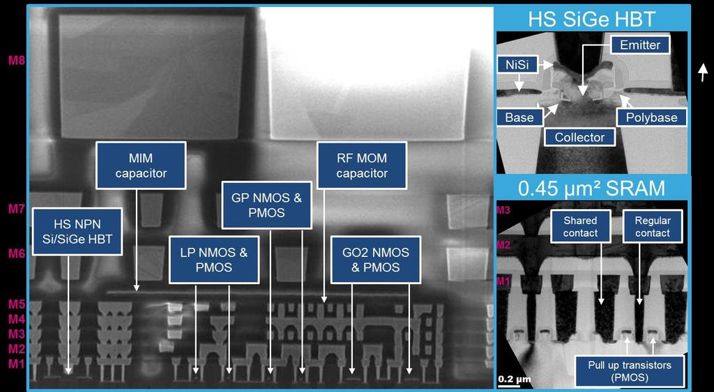
6 Technology cross-sections
7 BEOL schematic cross-section 9 metal layers (including Aluminum capping) BEOL obtained by the introduction of a thick Via/Line copper module : 3µm thick M8U and 1.5µm thick V7U MIM integrated in V5Z TFR integrated in V6Z All the 55-nm CMOS libraries are therefore compatible with BiCMOS055 CB Via7U Via6Z Via5Z Via4X BiCMOS055 8M4X2Z1U TFR MIM AP M8U M7Z M6Z M5X Via6Z Via5Z Via4X CMOS055 7M4X2Z0U AP M7Z M6Z M5X M2 to Last Metal Layer 5.5µm M1 polysi 3.1µm M1 polysi
8 BiCMOS055 devices list (DK2.3) Core LP/GP HVT & SVT CMOS w/ 2.5V GO2 (incl. RF SVT for LP, GP & GO2) High-Speed & Medium-Voltage SiGe HBTs Natural devices NPN & PNP bipolar transistors Resistors (active, poly & metal incl. RF resistors) Diodes (N+/Pwell, P+/Nwell, Deep Nwell/Psub, ) DC capacitors (poly, plate) Varactors Single & Diff. GO1/GO2 P+ poly/nwell varactors P+/Nwell diode varactor RF MOM MMW, HQ & LOHQ inductors µstrip transmission line Options LP & GP CMOS LVT (incl. RF models for LP & GP) SRAM SVT + HVT High-Performance Analog (HPA) CMOS (incl. RF models) High-Voltage SiGe HBTs 6k /sq. HIPO resistor (incl. RF model) 5fF/µm² MIM capacitor (incl. RF model) Thin Film Resistor Flip-Chip bumping
9 Devices targets LP & GP CMOS Low Power (LP) and General Purpose (GP) CMOS Device Low Power MOS (T OX =18.5Å) General Purpose MOS (T OX =13Å) I ON (µa/µm) I OFF (na/µm) I ON (µa/µm) I OFF (na/µm) Low V T NMOS Low V T PMOS Standard V T NMOS Standard V T PMOS High V T NMOS High V T PMOS L drawn =0.06µm, W drawn = 1.0 µm, T=25 C
10 Devices targets SiGe HBTs 3 collector flavors sharing the same E/B system Scalable emitter widths and lengths Device f T (GHz) f MAX (GHz) BV CBO (V) BV CEO (V) High-speed SiGe HBT schematic cross-section HS NPN SiGe HBT npnvhs, npnvhs_t 320 V CB =0.5V V BE =0.90V 370 V CB =0.5V V BE =0.90V 5.2 I CB =10µA 1.5 I B =0µA Pedestal oxide C C C B in-situ doped SiGe:C Base B E As in-situ doped Emitter B B doped Polybase C C C MV NPN SiGe HBT npnvmv, npnvmv_t 180 V CB =1.0V V BE =0.87V 380 V CB =1.0V V BE =0.87V 7.2 I CB =10µA 1.8 I B =0µA Localized Collector Collector Sinker HV NPN SiGe HBT npnvhv, npnvhv_t 70 V CB =2.0V V BE =0.80V 250 V CB =2.0V V BE =0.80V 13.5 I CB =10µA 3.2 I B =0µA Epitaxial Collector Buried Layer Shallow Trench Isolation (STI) Deep Trench Isolation (DTI) Double Polysilicon Self-Aligned (DPSA) architecture featuring a Selective Epitaxial Growth (SEG) of the base CBEBC: W drawn = 0.2 µm, L drawn =5.56µm, T=25 C
11 Devices targets Varactors & capacitors P+ Poly/NWell GO1 & GO2 benefit from short gate lengths Device Oxide type Capacitance range (Cmin / max) Typical tuning 25 C =100 ff Max C = V =1,2 V C =100 1,2 V 2,5 V (GO2) Varactor P+/NWell GO1 SE cpo12nw_var GO1 1,2 V 5 ff / 1 pf 3 (max 5) 20 > 110 GHz Varactor P+/NWell GO2 SE cpo25nw_var GO2 2,5 V 5 ff / 1 pf 3 (max 5) 30 > 110 GHz RF MOM MIM C 0 ~0.9 ff/µm² (M1-M2) to ~3.0 ffµm² (M1-M5) / C V1 < 1 ppm/v C 0 =5.0 ff/µm² / C V1 < 150 ppm/v / C V2 < 100 ppm/v²

: 1 to 4.25 From 65pH to 1.")


12 Devices targets Inductors & transmission lines Inductors & TL benefit from the 8ML BEOL with thick V7/M8 Device Stack L Qmax MMW Inductor ind_mmw_8m4x0y2z1u Inductors geometry: Coil M8U Upath M7Z Gnd ring M1 Number of coil turns (n): 1 to 4.25 From 65pH to 1.6nH Internal coil diameter (d): 10 to 50 µm Coil width (w): 0.6 to 4 µm Self resonance frequency > 10 From 27GHz to 300GHz 1-turn inductor 3D view M8 line 4.25-turn inductor 3D view Device Stack Zc IL M1 gnd µ-strip TL microstrip_8m4x0y2z1u Line in M8U Gnd in M1 or M4 From 35 to 70 Lateral wall 3D schematic view
13 All options are compatible with each other* Process options Masks count Masks count Core process 50 SRAM 3 Triple-V T Low-V T (LVT, SVT and HVT transistors) 2 High-Performance Analog (HPA) CMOS 2/4* HIPO (6k /sq poly resistor) 1 HV (High-Voltage) NPN 0 MIM (5fF/µm²) 2 TFR (Thin Film Resistor) 1 Flip-Chip 1 (*) HPA CMOS are LVT MOS devices. This option requires 2 masks in addition to LVT option, then 4 masks if standard LVT MOS devices are not used
14 Design kit & design platform
15 Design kit Front-end/Schematic capture EDA tools EDA Vendors Schematic Capture (Composer) IC Cadence Simulation model libraries Eldo Mentor Spectre Hspice Cadence Synopsys RF Simulation ADS (RFDE) Agilenteesof GoldenGate Agilenteesof ADS environment ADSKit ST Layout Entry & Finishing EDA tools EDA Vendors Layout Placement Virtuoso Layout Editor Cadence Layout Verification : DRC/LVS DFM YA/YE/YS Parasitic Extraction : interconnect RC Post Layout Simulation flow Calibre pvs StarRCXT ext PLSKit Totem Mentor Cadence Synopsys Cadence ST Apache

16 Design platform content

17 Design platform flows

18 Design platform version

19 Design flow
SiGe HBT Technology Development in the DOTSEVEN Project
 SiGe HBT Technology Development in the DOTSEVEN Project Alexander Fox 1, Bernd Heinemann 1, Josef Böck 2, Klaus Aufinger 2 1 IHP, 2 Infineon Technologies AG Open Bipolar Workshop 3 October 2013, Bordeaux
Lecture 020 ECE4430 Review II (1/5/04) Page 020-1
 Page 020-1") Lecture 020 ECE4430 Review II (1/5/04) Page 020-1 LECTURE 020 ECE 4430 REVIEW II (READING: GHLM - Chap. 2) Objective The objective of this presentation is: 1.) Identify the prerequisite material as taught
Lecture 020 ECE4430 Review II (1/5/04) Page 020-1 LECTURE 020 ECE 4430 REVIEW II (READING: GHLM - Chap. 2) Objective The objective of this presentation is: 1.) Identify the prerequisite material as taught
SiGe BiCMOS Technologies with RF and Photonic Modules
 INNOVATIONS FOR HIGH PERFORMANCE MICROELECTRONICS SiGe BiCMOS Technologies with RF and Photonic Modules Mul Project and Low Volume Wafer Produc on About Us IHP-GmbH is a German R & D institution, focused
Lecture 020 ECE4430 Review II (1/5/04) Page 020-1
 Page 020-1") Lecture 020 ECE4430 Review II (1/5/04) Page 020-1 LECTURE 020 ECE 4430 REVIEW II (READING: GHLM - Chap. 2) Objective The objective of this presentation is: 1.) Identify the prerequisite material as taught
Lecture 020 ECE4430 Review II (1/5/04) Page 020-1 LECTURE 020 ECE 4430 REVIEW II (READING: GHLM - Chap. 2) Objective The objective of this presentation is: 1.) Identify the prerequisite material as taught
F O U N D R Y L E A D E R S H I P F O R T H E S o C G E N E R A T I O N. Mixed-Signal/RFCMOS
 F O U N D R Y L E A D E R S H I P F O R T H E S o C G E N E R A T I O N www.umc.com Mixed-Signal/RFCMOS Solutions for Mixed-Signal/RFCMOS Applications Mixed-Signal and RFCMOS applications have become major
ST Technologies Snapshot for Analog & Mixed Laurent Dugoujon/Thibault BRUNET STMicroelectronics
 ST Technologies Snapshot for Analog & Mixed Laurent Dugoujon/Thibault BRUNET STMicroelectronics 1 Content Main technologies/applications BCD6s/BCD6s SOI BICMOS9MW HCMOS9A C065 Space Summary Perspectives
1 FUNDAMENTAL CONCEPTS What is Noise Coupling 1
 Contents 1 FUNDAMENTAL CONCEPTS 1 1.1 What is Noise Coupling 1 1.2 Resistance 3 1.2.1 Resistivity and Resistance 3 1.2.2 Wire Resistance 4 1.2.3 Sheet Resistance 5 1.2.4 Skin Effect 6 1.2.5 Resistance
Product Catalog. Semiconductor Intellectual Property & Technology Licensing Program
 Product Catalog Semiconductor Intellectual Property & Technology Licensing Program MANUFACTURING PROCESS TECHNOLOGY OVERVIEW 90 nm 130 nm 0.18 µm 0.25 µm 0.35 µm >0.40 µm Logic CMOS SOI CMOS SOI CMOS SOI
F O U N D R Y L E A D E R S H I P F O R T H E S o C G E N E R A T I O N. Mixed-Signal/RFCMOS
 F O U N D R Y L E A D E R S H I P F O R T H E S o C G E N E R A T I O N www.umc.com Mixed-Signal/RFCMOS Solutions for Mixed-Signal/RFCMOS Applications Mixed-Signal and RFCMOS applications have become major
Electronics Development for psec Time-of. of-flight Detectors. Enrico Fermi Institute University of Chicago. Fukun Tang
 Electronics Development for psec Time-of of-flight Detectors Fukun Tang Enrico Fermi Institute University of Chicago With Karen Byrum and Gary Drake (ANL) Henry Frisch, Mary Heintz and Harold Sanders (UC)
XI μm Process Family: The XI10 series is X-Fab's 1.0-micron Modular Silicon-On-Insulator Technology DESCRIPTION
 1.0 μm Process Family: XI10 The XI10 series is X-Fab's 1.0-micron Modular Silicon-On-Insulator Technology DESCRIPTION The XI10 series is X-FAB s 1.0 micron Modular Non-fully Depleted SOI CMOS Technology.
Chapter 3 Basics Semiconductor Devices and Processing
 Chapter 3 Basics Semiconductor Devices and Processing 1 Objectives Identify at least two semiconductor materials from the periodic table of elements List n-type and p-type dopants Describe a diode and
Chapter 3: Basics Semiconductor Devices and Processing 2006/9/27 1. Topics
 Chapter 3: Basics Semiconductor Devices and Processing 2006/9/27 1 Topics What is semiconductor Basic semiconductor devices Basics of IC processing CMOS technologies 2006/9/27 2 1 What is Semiconductor
+1 (479)
") Introduction to VLSI Design http://csce.uark.edu +1 (479) 575-6043 yrpeng@uark.edu Invention of the Transistor Vacuum tubes ruled in first half of 20th century Large, expensive, power-hungry, unreliable
Introduction to VLSI Design http://csce.uark.edu +1 (479) 575-6043 yrpeng@uark.edu Invention of the Transistor Vacuum tubes ruled in first half of 20th century Large, expensive, power-hungry, unreliable
INTEGRATED 0.18 MICRON RF TECHNOLOGY PLATFORM WITH 1.
 INTEGRATED 0.18 MICRON RF TECHNOLOGY PLATFORM WITH 1.8V 5V 12V 25V & 42V MOS FOR HIGH DIGITAL CONTENT POWER RF APPLICATIONS FEATURING FT = 55 GHZ RFMOS AND FT > 17 GHZ 12V RF-LDMOS. S. Levin, E. Aloni,
A New High Performance Complementary Bipolar Technology Featuring 45GHz NPN and 20GHz PNP Devices.
 A New High Performance Complementary Bipolar Technology Featuring 45GHz NPN and 20GHz PNP Devices. M C Wilson, P H Osborne, S Thomas and T Cook Mitel Semiconductor Cheney Manor, Swindon, Wiltshire, SN2
ECE 5745 Complex Digital ASIC Design Topic 2: CMOS Devices
 ECE 5745 Complex Digital ASIC Design Topic 2: CMOS Devices Christopher Batten School of Electrical and Computer Engineering Cornell University http://www.csl.cornell.edu/courses/ece5950 Simple Transistor
BCD Technology. Sense & Power and Automotive Technology R&D. January 2017
 BCD Technology Sense & Power and Automotive Technology R&D January 2017 Content 2 BCD in ST Technology platform details Content 3 BCD in ST Technology platform details What is BCD? 4 A concept invented
Integrated diodes. The forward voltage drop only slightly depends on the forward current. ELEKTRONIKOS ĮTAISAI
 1 Integrated diodes pn junctions of transistor structures can be used as integrated diodes. The choice of the junction is limited by the considerations of switching speed and breakdown voltage. The forward
Maxim MAX3940E Electro-Absorption Modulator Structural Analysis
 May 23, 2006 Maxim MAX3940E Electro-Absorption Modulator Structural Analysis For comments, questions, or more information about this report, or for any additional technical needs concerning semiconductor
Topic 3. CMOS Fabrication Process
 Topic 3 CMOS Fabrication Process Peter Cheung Department of Electrical & Electronic Engineering Imperial College London URL: www.ee.ic.ac.uk/pcheung/ E-mail: p.cheung@ic.ac.uk Lecture 3-1 Layout of a Inverter
Hot Topics and Cool Ideas in Scaled CMOS Analog Design
 Engineering Insights 2006 Hot Topics and Cool Ideas in Scaled CMOS Analog Design C. Patrick Yue ECE, UCSB October 27, 2006 Slide 1 Our Research Focus High-speed analog and RF circuits Device modeling,
Layout of a Inverter. Topic 3. CMOS Fabrication Process. The CMOS Process - photolithography (2) The CMOS Process - photolithography (1) v o.
 The CMOS Process - photolithography (1) v o.") Layout of a Inverter Topic 3 CMOS Fabrication Process V DD Q p Peter Cheung Department of Electrical & Electronic Engineering Imperial College London v i v o Q n URL: www.ee.ic.ac.uk/pcheung/ E-mail: p.cheung@ic.ac.uk
Layout of a Inverter Topic 3 CMOS Fabrication Process V DD Q p Peter Cheung Department of Electrical & Electronic Engineering Imperial College London v i v o Q n URL: www.ee.ic.ac.uk/pcheung/ E-mail: p.cheung@ic.ac.uk
F O U N D R Y L E A D E R S H I P F O R T H E S o C G E N E R A T I O N. Mixed-Signal/RFCMOS
 F O U N D R Y L E A D E R S H I P F O R T H E S o C G E N E R A T I O N www.umc.com Mixed-Signal/RFCMOS Solutions for Mixed-Signal/RFCMOS Applications Mixed-Signal and RFCMOS applications have become major
IFSIN. WEB PAGE Fall ://weble.upc.es/ifsin/
 IFSIN IMPLEMENTACIÓ FÍSICA DE SISTEMES INTEGRATS NANOMÈTRICS IMPLEMENTACIÓN N FÍSICA F DE SISTEMAS INTEGRADOS NANOMÉTRICOS PHYSICAL IMPLEMENTATION OF NANOMETER INTEGRATED SYSTEMS Fall 2008 Prof. Xavier
Basic Fabrication Steps
 Basic Fabrication Steps and Layout Somayyeh Koohi Department of Computer Engineering Adapted with modifications from lecture notes prepared by author Outline Fabrication steps Transistor structures Transistor
Wiring Parasitics. Contact Resistance Measurement and Rules
 Wiring Parasitics Contact Resistance Measurement and Rules Connections between metal layers and nonmetal layers are called contacts. Connections between metal layers are called vias. For non-critical design,
Jack Keil Wolf Lecture. ESE 570: Digital Integrated Circuits and VLSI Fundamentals. Lecture Outline. MOSFET N-Type, P-Type.
 ESE 570: Digital Integrated Circuits and VLSI Fundamentals Jack Keil Wolf Lecture Lec 3: January 24, 2019 MOS Fabrication pt. 2: Design Rules and Layout http://www.ese.upenn.edu/about-ese/events/wolf.php
Fabrication, Corner, Layout, Matching, & etc.
 Advanced Analog Building Blocks Fabrication, Corner, Layout, Matching, & etc. Wei SHEN (KIP) 1 Fabrication Steps for MOS Wei SHEN, Universität Heidelberg 2 Fabrication Steps for MOS Wei SHEN, Universität
ESE 570: Digital Integrated Circuits and VLSI Fundamentals
 ESE 570: Digital Integrated Circuits and VLSI Fundamentals Lec 3: January 24, 2019 MOS Fabrication pt. 2: Design Rules and Layout Penn ESE 570 Spring 2019 Khanna Jack Keil Wolf Lecture http://www.ese.upenn.edu/about-ese/events/wolf.php
ITRS: RF and Analog/Mixed- Signal Technologies for Wireless Communications. Nick Krajewski CMPE /16/2005
 ITRS: RF and Analog/Mixed- Signal Technologies for Wireless Communications Nick Krajewski CMPE 640 11/16/2005 Introduction 4 Working Groups within Wireless Analog and Mixed Signal (0.8 10 GHz) (Covered
Intel Xeon E3-1230V2 CPU Ivy Bridge Tri-Gate 22 nm Process
 Intel Xeon E3-1230V2 CPU Structural Analysis 3685 Richmond Road, Suite 500, Ottawa, ON K2H 5B7 Canada Tel: 613-829-0414 www.chipworks.com Structural Analysis Some of the information in this report may
Chapter 2 : Semiconductor Materials & Devices (II) Feb
 Feb") Chapter 2 : Semiconductor Materials & Devices (II) 1 Reference 1. SemiconductorManufacturing Technology: Michael Quirk and Julian Serda (2001) 3. Microelectronic Circuits (5/e): Sedra & Smith (2004) 4.
Chapter 2 : Semiconductor Materials & Devices (II) 1 Reference 1. SemiconductorManufacturing Technology: Michael Quirk and Julian Serda (2001) 3. Microelectronic Circuits (5/e): Sedra & Smith (2004) 4.
Technology Overview. MM-Wave SiGe IC Design
 Sheet Code RFi0606 Technology Overview MM-Wave SiGe IC Design Increasing consumer demand for high data-rate wireless applications has resulted in development activity to exploit the mm-wave frequency range
THERE is currently a great deal of activity directed toward
 IEEE JOURNAL OF SOLID-STATE CIRCUITS, VOL. 32, NO. 12, DECEMBER 1997 2097 A 2.5-GHz BiCMOS Transceiver for Wireless LAN s Robert G. Meyer, Fellow IEEE, William D. Mack, Senior Member IEEE, and Johannes
2.8 - CMOS TECHNOLOGY
 CMOS Technology (6/7/00) Page 1 2.8 - CMOS TECHNOLOGY INTRODUCTION Objective The objective of this presentation is: 1.) Illustrate the fabrication sequence for a typical MOS transistor 2.) Show the physical
Chapter 1. Introduction
 EECS3611 Analog Integrated Circuit esign Chapter 1 Introduction EECS3611 Analog Integrated Circuit esign Instructor: Prof. Ebrahim Ghafar-Zadeh, Prof. Peter Lian email: egz@cse.yorku.ca peterlian@cse.yorku.ca
DATASHEET CADENCE QRC EXTRACTION
 DATASHEET Cadence QRC Etraction, the industry s premier 3D fullchip parasitic etractor that is independent of design style or flow, is a fast and accurate RLCK etraction solution used during design implementation
Device Technologies. Yau - 1
 Device Technologies Yau - 1 Objectives After studying the material in this chapter, you will be able to: 1. Identify differences between analog and digital devices and passive and active components. Explain
A 90 nm High Volume Manufacturing Logic Technology Featuring Novel 45 nm Gate Length Strained Silicon CMOS Transistors
 A 90 nm High Volume Manufacturing Logic Technology Featuring Novel 45 nm Gate Length Strained Silicon CMOS Transistors T. Ghani, M. Armstrong, C. Auth, M. Bost, P. Charvat, G. Glass, T. Hoffmann*, K. Johnson#,
Indium Phosphide and Related Materials Selectively implanted subcollector DHBTs
 Indium Phosphide and Related Materials - 2006 Selectively implanted subcollector DHBTs Navin Parthasarathy, Z. Griffith, C. Kadow, U. Singisetti, and M.J.W. Rodwell Dept. of Electrical and Computer Engineering,
AMICSA Bridging Science & Applications F r o m E a r t h t o S p a c e a n d b a c k. Kayser-Threde GmbH. Space
 Bridging Science & Applications F r o m E a r t h t o S p a c e a n d b a c k E a r t h S p a c e & F u t u r e Kayser-Threde GmbH Space Industrial Applications AMICSA 2008 First radiation test results
RADIO FREQUENCY 2003 EDITION AND ANALOG/MIXED-SIGNAL TECHNOLOGIES FOR WIRELESS COMMUNICATIONS [A SECTION OF THE PROCESS INTEGRATION CHAPTER]
![RADIO FREQUENCY 2003 EDITION AND ANALOG/MIXED-SIGNAL TECHNOLOGIES FOR WIRELESS COMMUNICATIONS [A SECTION OF THE PROCESS INTEGRATION CHAPTER]](/thumbs/91/105542220.jpg "RADIO FREQUENCY 2003 EDITION AND ANALOG/MIXED-SIGNAL TECHNOLOGIES FOR WIRELESS COMMUNICATIONS [A SECTION OF THE PROCESS INTEGRATION CHAPTER]") I NTERNATIONAL TECHNOLOGY R OADMAP FOR SEMICONDUCTORS 2003 EDITION RADIO FREQUENCY AND ANALOG/MIXED-SIGNAL TECHNOLOGIES FOR WIRELESS COMMUNICATIONS [A SECTION OF THE PROCESS INTEGRATION CHAPTER] THE ITRS
I NTERNATIONAL TECHNOLOGY R OADMAP FOR SEMICONDUCTORS 2003 EDITION RADIO FREQUENCY AND ANALOG/MIXED-SIGNAL TECHNOLOGIES FOR WIRELESS COMMUNICATIONS [A SECTION OF THE PROCESS INTEGRATION CHAPTER] THE ITRS
Wafer-scale 3D integration of silicon-on-insulator RF amplifiers
 Wafer-scale integration of silicon-on-insulator RF amplifiers The MIT Faculty has made this article openly available. Please share how this access benefits you. Your story matters. Citation As Published
6.776 High Speed Communication Circuits Lecture 6 MOS Transistors, Passive Components, Gain- Bandwidth Issue for Broadband Amplifiers
 6.776 High Speed Communication Circuits Lecture 6 MOS Transistors, Passive Components, Gain- Bandwidth Issue for Broadband Amplifiers Massachusetts Institute of Technology February 17, 2005 Copyright 2005
Quantum-effect Resonant Tunneling Device Technology for Practical Ultra Low-power High-speed Applications
 Quantum-effect Resonant Tunneling Device Technology for Practical Ultra Low-power High-speed Applications SEMATECH Symposium October 23 rd, 2012 Prof. Kyounghoon Yang High Speed Nanoelectronics Laboratory
Streamlined Design of SiGe Based Power Amplifiers
 ROMANIAN JOURNAL OF INFORMATION SCIENCE AND TECHNOLOGY Volume 13, Number 1, 2010, 22 32 Streamlined Design of SiGe Based Power Amplifiers Mladen BOŽANIĆ1, Saurabh SINHA 1, Alexandru MÜLLER2 1 Department
Study the Analysis of Low power and High speed CMOS Logic Circuits in 90nm Technology
 43 Study the Analysis of Low power and High speed CMOS Logic Circuits in 90nm Technology Fazal Noorbasha 1, Ashish Verma 1 and A.M. Mahajan 2 1. Laboratory of VLSI and Embedded Systems, Deptt. Of Physics
Integrated Circuit Amplifiers. Comparison of MOSFETs and BJTs
 Integrated Circuit Amplifiers Comparison of MOSFETs and BJTs 17 Typical CMOS Device Parameters 0.8 µm 0.25 µm 0.13 µm Parameter NMOS PMOS NMOS PMOS NMOS PMOS t ox (nm) 15 15 6 6 2.7 2.7 C ox (ff/µm 2 )
Chapter 4.5. High Frequency Passive Devices
 Chapter 4.5. High Frequency Passive Devices 1 Outline Inductors Transmission lines Varactors MIM Capacitors Resistors 2 Types of integrated inductors (Yoon, RFIC-2003) In silicon ICs: Spiral Multi-layer
Semiconductor Memory: DRAM and SRAM. Department of Electrical and Computer Engineering, National University of Singapore
 Semiconductor Memory: DRAM and SRAM Outline Introduction Random Access Memory (RAM) DRAM SRAM Non-volatile memory UV EPROM EEPROM Flash memory SONOS memory QD memory Introduction Slow memories Magnetic
Introduction to VLSI ASIC Design and Technology
 Introduction to VLSI ASIC Design and Technology Paulo Moreira CERN - Geneva, Switzerland Paulo Moreira Introduction 1 Outline Introduction Is there a limit? Transistors CMOS building blocks Parasitics
EE4800 CMOS Digital IC Design & Analysis. Lecture 1 Introduction Zhuo Feng
 EE4800 CMOS Digital IC Design & Analysis Lecture 1 Introduction Zhuo Feng 1.1 Prof. Zhuo Feng Office: EERC 730 Phone: 487-3116 Email: zhuofeng@mtu.edu Class Website http://www.ece.mtu.edu/~zhuofeng/ee4800fall2010.html
Monolithic Pixel Detector in a 0.15µm SOI Technology
 Monolithic Pixel Detector in a 0.15µm SOI Technology 2006 IEEE Nuclear Science Symposium, San Diego, California, Nov. 1, 2006 Yasuo Arai (KEK) KEK Detector Technology Project : [SOIPIX Group] Y. Arai Y.
VLSI Technology Dr. Nandita Dasgupta Department of Electrical Engineering Indian Institute of Technology, Madras
 VLSI Technology Dr. Nandita Dasgupta Department of Electrical Engineering Indian Institute of Technology, Madras Lecture - 40 BICMOS technology So, today we are going to have the last class on this VLSI
BipAK 2014 Experience of BE Tunneling current and BC Barrier effect with HICUM L2 v2.32
 1 BipAK 2014 Experience of BE Tunneling current and BC Barrier effect with HICUM L2 v2.32 Nicolas Derrier October 2014 ref. dm14.161 Outline 2 HICUM Level2 v2.32 Experience with Tunnel current Experience
Using Sonnet EM Analysis with Cadence Virtuoso in RFIC Design. Sonnet Application Note: SAN-201B July 2011
 Using Sonnet EM Analysis with Cadence Virtuoso in RFIC Design Sonnet Application Note: SAN-201B July 2011 Description of Sonnet Suites Professional Sonnet Suites Professional is an industry leading full-wave
95GHz Receiver with Fundamental Frequency VCO and Static Frequency Divider in 65nm Digital CMOS
 95GHz Receiver with Fundamental Frequency VCO and Static Frequency Divider in 65nm Digital CMOS Ekaterina Laskin, Mehdi Khanpour, Ricardo Aroca, Keith W. Tang, Patrice Garcia 1, Sorin P. Voinigescu University
Structured LNA Design for Next Generation Mobile Communication
 Structured LNA Design for Next Generation Mobile Communication Master of Science Thesis in the Master Degree Program Radio and Space Science Engineering Sohaib Maalik Department of Microtechnology and
A 2.4-GHz 24-dBm SOI CMOS Power Amplifier with Fully Integrated Output Balun and Switched Capacitors for Load Line Adaptation
 A 2.4-GHz 24-dBm SOI CMOS Power Amplifier with Fully Integrated Output Balun and Switched Capacitors for Load Line Adaptation Francesco Carrara 1, Calogero D. Presti 2,1, Fausto Pappalardo 1, and Giuseppe
PHYSICAL STRUCTURE OF CMOS INTEGRATED CIRCUITS. Dr. Mohammed M. Farag
 PHYSICAL STRUCTURE OF CMOS INTEGRATED CIRCUITS Dr. Mohammed M. Farag Outline Integrated Circuit Layers MOSFETs CMOS Layers Designing FET Arrays EE 432 VLSI Modeling and Design 2 Integrated Circuit Layers
Seminar report Bicmos Technology
 A Seminar report On Bicmos Technology Submitted in partial fulfillment of the requirement for the award of degree of Bachelor of Technology in Mechanical SUBMITTED TO: SUBMITTED BY: Acknowledgement I would
420 Intro to VLSI Design
 Dept of Electrical and Computer Engineering 420 Intro to VLSI Design Lecture 0: Course Introduction and Overview Valencia M. Joyner Spring 2005 Getting Started Syllabus About the Instructor Labs, Problem
! Review: MOS IV Curves and Switch Model. ! MOS Device Layout. ! Inverter Layout. ! Gate Layout and Stick Diagrams. ! Design Rules. !
 ESE 570: Digital Integrated Circuits and VLSI Fundamentals Lec 3: January 21, 2016 MOS Fabrication pt. 2: Design Rules and Layout Lecture Outline! Review: MOS IV Curves and Switch Model! MOS Device Layout!
ESE 570: Digital Integrated Circuits and VLSI Fundamentals
 ESE 570: Digital Integrated Circuits and VLSI Fundamentals Lec 3: January 21, 2016 MOS Fabrication pt. 2: Design Rules and Layout Penn ESE 570 Spring 2016 Khanna Adapted from GATech ESE3060 Slides Lecture
CMOS Digital Integrated Circuits Lec 2 Fabrication of MOSFETs
 CMOS Digital Integrated Circuits Lec 2 Fabrication of MOSFETs 1 CMOS Digital Integrated Circuits 3 rd Edition Categories of Materials Materials can be categorized into three main groups regarding their
VLSI Design. Introduction
 VLSI Design Introduction Outline Introduction Silicon, pn-junctions and transistors A Brief History Operation of MOS Transistors CMOS circuits Fabrication steps for CMOS circuits Introduction Integrated
ECEN474/704: (Analog) VLSI Circuit Design Fall 2016
 VLSI Circuit Design Fall 2016") ECEN474/704: (Analog) VLSI Circuit Design Fall 2016 Lecture 1: Introduction Sam Palermo Analog & Mixed-Signal Center Texas A&M University Announcements Turn in your 0.18um NDA form by Thursday Sep 1 No
ECEN474/704: (Analog) VLSI Circuit Design Fall 2016 Lecture 1: Introduction Sam Palermo Analog & Mixed-Signal Center Texas A&M University Announcements Turn in your 0.18um NDA form by Thursday Sep 1 No
TU3B-1. An 81 GHz, 470 mw, 1.1 mm 2 InP HBT Power Amplifier with 4:1 Series Power Combining using Sub-quarter-wavelength Baluns
 TU3B-1 Student Paper Finalist An 81 GHz, 470 mw, 1.1 mm 2 InP HBT Power Amplifier with 4:1 Series Power Combining using Sub-quarter-wavelength Baluns H. Park 1, S. Daneshgar 1, J. C. Rode 1, Z. Griffith
ECEN474: (Analog) VLSI Circuit Design Fall 2011
 VLSI Circuit Design Fall 2011") ECEN474: (Analog) VLSI Circuit Design Fall 2011 Lecture 1: Introduction Sebastian Hoyos Analog & Mixed-Signal Center Texas A&M University Analog Circuit Sequence 326 2 Why is Analog Important? [Silva]
ECEN474: (Analog) VLSI Circuit Design Fall 2011 Lecture 1: Introduction Sebastian Hoyos Analog & Mixed-Signal Center Texas A&M University Analog Circuit Sequence 326 2 Why is Analog Important? [Silva]
Signal Integrity Design of TSV-Based 3D IC
 Signal Integrity Design of TSV-Based 3D IC October 24, 21 Joungho Kim at KAIST joungho@ee.kaist.ac.kr http://tera.kaist.ac.kr 1 Contents 1) Driving Forces of TSV based 3D IC 2) Signal Integrity Issues
VLSI Design. Introduction
 Tassadaq Hussain VLSI Design Introduction Outcome of this course Problem Aims Objectives Outcomes Data Collection Theoretical Model Mathematical Model Validate Development Analysis and Observation Pseudo
EE 330 Lecture 21. Bipolar Process Flow
 EE 330 Lecture 21 Bipolar Process Flow Exam 2 Friday March 9 Exam 3 Friday April 13 Review from Last Lecture Simplified Multi-Region Model I C βi B JSA IB β V 1 V E e V CE BE V t AF V BE >0.4V V BC
Lecture 0: Introduction
 Lecture 0: Introduction Introduction Integrated circuits: many transistors on one chip. Very Large Scale Integration (VLSI): bucketloads! Complementary Metal Oxide Semiconductor Fast, cheap, low power
ON-CHIP TECHNOLOGY INDEPENDENT 3-D MOD- ELS FOR MILLIMETER-WAVE TRANSMISSION LINES WITH BEND AND GAP DISCONTINUITY
 Progress In Electromagnetics Research B, Vol. 22, 171 185, 2010 ON-CHIP TECHNOLOGY INDEPENDENT 3-D MOD- ELS FOR MILLIMETER-WAVE TRANSMISSION LINES WITH BEND AND GAP DISCONTINUITY G. A. Wang, W. Woods,
EM Analysis of RFIC Inductors and Transformers. Dr.-Ing. Volker Mühlhaus Dr. Mühlhaus Consulting & Software GmbH, Witten
 EM Analysis of RFIC Inductors and Transformers Dr.-Ing. Volker Mühlhaus, Witten Do you love inductors? Image Kansas State University Inductors from the design kit tend to have the wrong value, optimized
techniques, and gold metalization in the fabrication of this device.
 Up to 6 GHz Medium Power Silicon Bipolar Transistor Chip Technical Data AT-42 Features High Output Power: 21. dbm Typical P 1 db at 2. GHz 2.5 dbm Typical P 1 db at 4. GHz High Gain at 1 db Compression:
Advanced Digital Integrated Circuits. Lecture 2: Scaling Trends. Announcements. No office hour next Monday. Extra office hour Tuesday 2-3pm
 EE241 - Spring 20 Advanced Digital Integrated Circuits Lecture 2: Scaling Trends and Features of Modern Technologies Announcements No office hour next Monday Extra office hour Tuesday 2-3pm 2 1 Outline
65-GHz Receiver in SiGe BiCMOS Using Monolithic Inductors and Transformers
 65-GHz Receiver in SiGe BiCMOS Using Monolithic Inductors and Transformers Michael Gordon, Terry Yao, Sorin P. Voinigescu University of Toronto March 10 2006, UBC, Vancouver Outline Motivation mm-wave
Up to 6 GHz Low Noise Silicon Bipolar Transistor Chip. Technical Data AT-41400
 Up to 6 GHz Low Noise Silicon Bipolar Transistor Chip Technical Data AT-1 Features Low Noise Figure: 1.6 db Typical at 3. db Typical at. GHz High Associated Gain: 1.5 db Typical at 1.5 db Typical at. GHz
CS/ECE 5710/6710. Composite Layout
 CS/ECE 5710/6710 Introduction to Layout Inverter Layout Example Layout Design Rules Composite Layout Drawing the mask layers that will be used by the fabrication folks to make the devices Very different
EE241 - Spring 2013 Advanced Digital Integrated Circuits. Projects. Groups of 3 Proposals in two weeks (2/20) Topics: Lecture 5: Transistor Models
 Topics: Lecture 5: Transistor Models") EE241 - Spring 2013 Advanced Digital Integrated Circuits Lecture 5: Transistor Models Projects Groups of 3 Proposals in two weeks (2/20) Topics: Soft errors in datapaths Soft errors in memory Integration
EE241 - Spring 2013 Advanced Digital Integrated Circuits Lecture 5: Transistor Models Projects Groups of 3 Proposals in two weeks (2/20) Topics: Soft errors in datapaths Soft errors in memory Integration
Microelectronics, BSc course
 Microelectronics, BSc course MOS circuits: CMOS circuits, construction http://www.eet.bme.hu/~poppe/miel/en/14-cmos.pptx http://www.eet.bme.hu The abstraction level of our study: SYSTEM + MODULE GATE CIRCUIT
! Review: MOS IV Curves and Switch Model. ! MOS Device Layout. ! Inverter Layout. ! Gate Layout and Stick Diagrams. ! Design Rules. !
 ESE 570: Digital Integrated Circuits and VLSI Fundamentals Lec 3: January 21, 2017 MOS Fabrication pt. 2: Design Rules and Layout Lecture Outline! Review: MOS IV Curves and Switch Model! MOS Device Layout!
Introducing 10-nm FinFET technology in Microwind
 Introducing 10-nm FinFET technology in Microwind Etienne Sicard To cite this version: Etienne Sicard. Introducing 10-nm FinFET technology in Microwind. This paper describes the implementation of a high
The 3D Silicon Leader
 The 3D Silicon Leader 3D Silicon IPD for smaller and more reliable Implantable Medical Devices ATW on Advanced Packaging for Wireless Medical Devices Mohamed Mehdi Jatlaoui, Sébastien Leruez, Olivier Gaborieau,
EECS130 Integrated Circuit Devices
 EECS130 Integrated Circuit Devices Professor Ali Javey 11/6/2007 MOSFETs Lecture 6 BJTs- Lecture 1 Reading Assignment: Chapter 10 More Scalable Device Structures Vertical Scaling is important. For example,
BiCMOS Circuit Design
 BiCMOS Circuit Design 1. Introduction to BiCMOS 2. Process, Device, and Modeling 3. BiCMOS Digital Circuit Design 4. BiCMOS Analog Circuit Design 5. BiCMOS Subsystems and Practical Considerations Tai-Haur
Lecture 190 CMOS Technology, Compatible Devices (10/28/01) Page 190-1
 Page 190-1") Lecture 190 CMOS Technology, Compatible Devices (10/28/01) Page 190-1 LECTURE 190 CMOS TECHNOLOGY-COMPATIBLE DEVICES (READING: Text-Sec. 2.9) INTRODUCTION Objective The objective of this presentation is
Lecture 190 CMOS Technology, Compatible Devices (10/28/01) Page 190-1 LECTURE 190 CMOS TECHNOLOGY-COMPATIBLE DEVICES (READING: Text-Sec. 2.9) INTRODUCTION Objective The objective of this presentation is
Lecture: Integration of silicon photonics with electronics. Prepared by Jean-Marc FEDELI CEA-LETI
 Lecture: Integration of silicon photonics with electronics Prepared by Jean-Marc FEDELI CEA-LETI Context The goal is to give optical functionalities to electronics integrated circuit (EIC) The objectives
30 ma flash LDO voltage regulator (output voltage 1.8 ± 0.2 V)
") SPECIFICATION 1 FEATURES Global Foundries CMOS 55 nm Low drop out Low current consumption Two modes operations: Normal, Economy Mode operation Bypass No discrete filtering capacitors required (cap-less
SPECIFICATION 1 FEATURES Global Foundries CMOS 55 nm Low drop out Low current consumption Two modes operations: Normal, Economy Mode operation Bypass No discrete filtering capacitors required (cap-less
Active Technology for Communication Circuits
 EECS 242: Active Technology for Communication Circuits UC Berkeley EECS 242 Copyright Prof. Ali M Niknejad Outline Comparison of technology choices for communication circuits Si npn, Si NMOS, SiGe HBT,
BCD Smart Power Roadmap Trends and Challenges. Giuseppe Croce NEREID WORKSHOP Smart Energy Bertinoro, October 20 th
 BCD Smart Power Roadmap Trends and Challenges Giuseppe Croce NEREID WORKSHOP Smart Energy Bertinoro, October 20 th Outline 2 Introduction Major Trends in Smart Power ASICs An insight on (some) differentiating
A SPAD-Based, Direct Time-of-Flight, 64 Zone, 15fps, Parallel Ranging Device Based on 40nm CMOS SPAD Technology
 A SPAD-Based, Direct Time-of-Flight, 64 Zone, 15fps, Parallel Ranging Device Based on 40nm CMOS SPAD Technology Pascal Mellot / Bruce Rae 27 th February 2018 Summary 2 Introduction to ranging device Summary
Integrated Circuits: FABRICATION & CHARACTERISTICS - 4. Riju C Issac
 Integrated Circuits: FABRICATION & CHARACTERISTICS - 4 Riju C Issac INTEGRATED RESISTORS Resistor in a monolithic IC is very often obtained by the bulk resistivity of one of the diffused areas. P-type
Design of a Low Noise Amplifier using 0.18µm CMOS technology
 The International Journal Of Engineering And Science (IJES) Volume 4 Issue 6 Pages PP.11-16 June - 2015 ISSN (e): 2319 1813 ISSN (p): 2319 1805 Design of a Low Noise Amplifier using 0.18µm CMOS technology
Silicon Avalanche Photodetectors Fabricated With Standard CMOS/BiCMOS Technology Myung-Jae Lee
 Silicon Avalanche Photodetectors Fabricated With Standard CMOS/BiCMOS Technology Myung-Jae Lee The Graduate School Yonsei University Department of Electrical and Electronic Engineering Silicon Avalanche
30% PAE W-band InP Power Amplifiers using Sub-quarter-wavelength Baluns for Series-connected Power-combining
 2013 IEEE Compound Semiconductor IC Symposium, October 13-15, Monterey, C 30% PAE W-band InP Power Amplifiers using Sub-quarter-wavelength Baluns for Series-connected Power-combining 1 H.C. Park, 1 S.
Low-Power VLSI. Seong-Ook Jung VLSI SYSTEM LAB, YONSEI University School of Electrical & Electronic Engineering
 Low-Power VLSI Seong-Ook Jung 2013. 5. 27. sjung@yonsei.ac.kr VLSI SYSTEM LAB, YONSEI University School of Electrical & Electronic Engineering Contents 1. Introduction 2. Power classification & Power performance
An Inductor-Based 52-GHz 0.18 µm SiGe HBT Cascode LNA with 22 db Gain
 An Inductor-Based 52-GHz 0.18 µm SiGe HBT Cascode LNA with 22 db Gain Michael Gordon, Sorin P. Voinigescu University of Toronto Toronto, Ontario, Canada ESSCIRC 2004, Leuven, Belgium Outline Motivation