EECS130 Integrated Circuit Devices
|
|
|
- Sabina Farmer
- 5 years ago
- Views:
Transcription
1 EECS130 Integrated Circuit Devices Professor Ali Javey 11/6/2007 MOSFETs Lecture 6 BJTs- Lecture 1 Reading Assignment: Chapter 10
2 More Scalable Device Structures Vertical Scaling is important. For example, reducing T ox gives the gate excellent control of Si surface potential. But, the drain could still have more control than the gate along another leakage current path that is some distance below the Si surface. (Right figure.) V gs T ox C g V ds S D N+ C g C d C d P-Sub leakage path
.")

3 Ultra-Thin-Body (UTB) MOSFET MOSFET built on very thin silicon film on an insulator (SiO 2 ). Since the silicon film is very thin, perhaps less than 10nm, no leakage path is very far from the gate. Electron Micrograph of UTB MOSFET Gate Gate N + N + SiO 2 Source SiO 2 Si Drain T Si = 3 nm


4 New Structure I--Ultra-Thin-Body MOSFET The subthreshold leakage is reduced as the silicon film is made thinner. T ox =1.5nm, N sub =1e15cm -3, V dd =1V, V gs =0

5 Preparation of Silicon-on-Insulator (SOI) Substrate Initial Silicon wafer A and B Oxidize wafer A to grow SiO2 Implant hydrogen into wafer A Place wafer A, upside down, over wafer B. A low temperature annealing causes the two wafers to fuse together. Apply another annealing step to for H 2 bubbles and split wafer A. Polish the surface and the SOI wafer is ready for use. Wafer A can be reused.

6 Cross-Section of SOI Circuits Buried Oxide Si Due to the high cost of SOI wafers, only some microprocessors, which command high prices and compete on speed, have embraced this technology. In order to benefit from the UTB concept, Si film thickness must be agreesively reduced to ~ Lg/4
7 New Struture II--Multi-Gate MOSFET and FinFET The second way of eliminating deep leakage paths is to provide gate control from more than one side of the channel. The Si film is very thin so that no leakage path is far from one of the gates. Because there are more than one gates, the structure may be called multi-gate MOSFET. Gate 1 V g Source Si Drain T Si T ox Gate 2 double-gate MOSFET
8 FinFET One multi-gate structure, called FinFET, is particularly attractive for its simplicity of fabrication. Called FinFET because its silicon body resembles the back fin of a fish. The channel consists of the two vertical surfaces and the top surface of the fin. Gate Source Drain Question: What is the channel width, W? Answer: The sum of twice the fin height and the width of the fin. Source L g
9 FinFET Process Flow Si Fin Resist BOX Si 3 N 4 Spacer SOI Substrate Fin Patterning Poly Poly Gate Deposition/Litho NiSi Gate Etch Spacer Formation S/D Implant + RTA Silicidation
10 Variations of FinFET G S D L g S D G S G D Buried Oxide Tall FinFET T si Short FinFET Nanowire FinFET Tall FinFET has the advantage of providing a large W and therefore large I on while occupying a small footprint. Short FinFET has the advantage of less challenging lithography and etching. Nanowire FinFET gives the gate even more control over the silicon wire by surrounding it.


11 Tall FinFET with L g =10nm Poly-Si Si Fin NiSi 220Å SiO2 cap Lg=10nm BOX B. Yu et al., IEDM 2002


12 Nanowire FinFET 5nm Gate Length F. Yang et al., 2004 VLSI Tech Symp. S G D L g = 5 nm S G D
13 Device Simulation and Process Simulation Device Simulation Commercially available computer simulation tools can solve all the equations presented in this book simultaneously with few or no approximations. Device simulation provides quick feedback about device design before long and expensive fabrication. Process Simulation Inputs to process simulation: lithography mask pattern, implantation dose and energy, temperatures and times for oxidization and annealing steps, etc. The process simulator generates a 2-D or 3-D structures with all the deposited or grown and etched thin films and doped regions. This output may be fed into a device simulator as input together with applied voltages.


. There are more more subthreshold inversion")
14 Example of Device Simulation--- Density of Inversion Charge in the Cross-Section of a FinFET Body S G D C.-H. Lin et al., 2005 SRC TECHCON Tall FinFET Short FinFET The inversion layer has a significant thickness (T ch ). There are more more subthreshold inversion electrons at the corners.


15 FinFET Process Example of Process Simulation The small figures only show 1/4 of the complete FinFET- -the quarter farthest from the viewer. Manual, Taurus Process, Synoposys Inc.
16 Bipolar Junction Transistors (BJTs) Since 1970, the high density and low-power advantage of the MOS technology steadily eroded the BJT s early dominance. BJTs are still preferred in some high-frequency and analog applications because of their high transconductance and high speed.
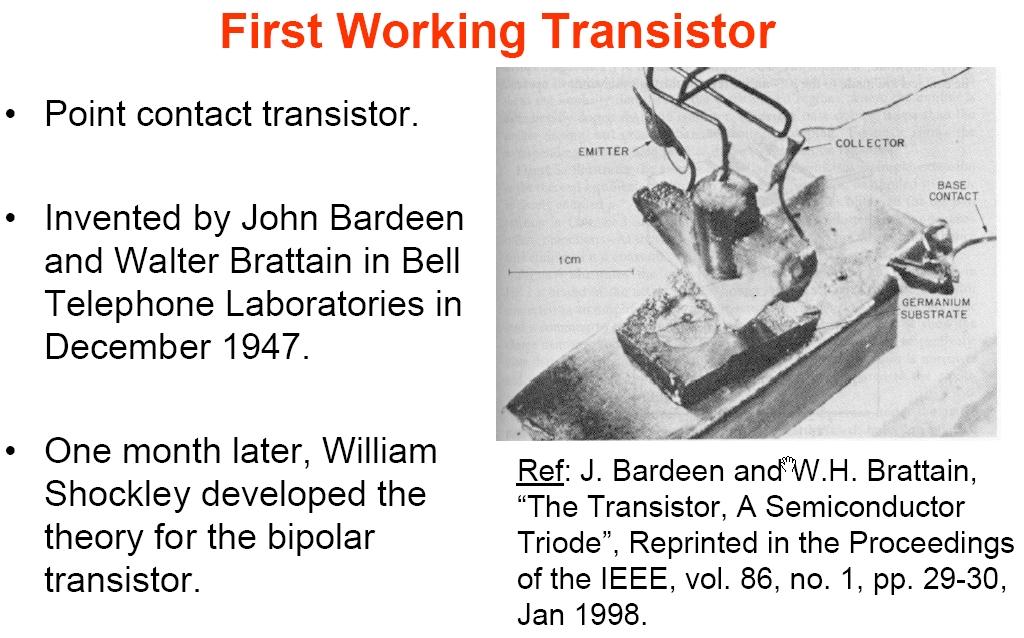
17
18
19 Schematic representation of pnp and npn BJTs Emitter is heavily doped compared to collector. So, emitter and collector are not interchangeable. The base width is small compared to the minority carrier diffusion length. If the base is much larger, then this will behave like back-to-back diodes.
EECS130 Integrated Circuit Devices
 EECS130 Integrated Circuit Devices Professor Ali Javey 11/01/2007 MOSFETs Lecture 5 Announcements HW7 set is due now HW8 is assigned, but will not be collected/graded. MOSFET Technology Scaling Technology
Lecture 27 ANNOUNCEMENTS. Regular office hours will end on Monday 12/10 Special office hours will be posted on the EE105 website
 Lecture 27 ANNOUNCEMENTS Regular office hours will end on Monday 12/10 Special office hours will be posted on the EE105 website Final Exam Review Session: Friday 12/14, 3PM, HP Auditorium Video will be
EE 5611 Introduction to Microelectronic Technologies Fall Thursday, September 04, 2014 Lecture 02
 EE 5611 Introduction to Microelectronic Technologies Fall 2014 Thursday, September 04, 2014 Lecture 02 1 Lecture Outline Review on semiconductor materials Review on microelectronic devices Example of microelectronic
Fin-Shaped Field Effect Transistor (FinFET) Min Ku Kim 03/07/2018
 Min Ku Kim 03/07/2018") Fin-Shaped Field Effect Transistor (FinFET) Min Ku Kim 03/07/2018 ECE 658 Sp 2018 Semiconductor Materials and Device Characterizations OUTLINE Background FinFET Future Roadmap Keeping up w/ Moore s Law
Fin-Shaped Field Effect Transistor (FinFET) Min Ku Kim 03/07/2018 ECE 658 Sp 2018 Semiconductor Materials and Device Characterizations OUTLINE Background FinFET Future Roadmap Keeping up w/ Moore s Law
Lecture 020 ECE4430 Review II (1/5/04) Page 020-1
 Page 020-1") Lecture 020 ECE4430 Review II (1/5/04) Page 020-1 LECTURE 020 ECE 4430 REVIEW II (READING: GHLM - Chap. 2) Objective The objective of this presentation is: 1.) Identify the prerequisite material as taught
Lecture 020 ECE4430 Review II (1/5/04) Page 020-1 LECTURE 020 ECE 4430 REVIEW II (READING: GHLM - Chap. 2) Objective The objective of this presentation is: 1.) Identify the prerequisite material as taught
I E I C since I B is very small
 Figure 2: Symbols and nomenclature of a (a) npn and (b) pnp transistor. The BJT consists of three regions, emitter, base, and collector. The emitter and collector are usually of one type of doping, while
FinFET-based Design for Robust Nanoscale SRAM
 FinFET-based Design for Robust Nanoscale SRAM Prof. Tsu-Jae King Liu Dept. of Electrical Engineering and Computer Sciences University of California at Berkeley Acknowledgements Prof. Bora Nikoli Zheng
3-D Modelling of the Novel Nanoscale Screen-Grid Field Effect Transistor (SGFET)
") 3-D Modelling of the Novel Nanoscale Screen-Grid Field Effect Transistor (SGFET) Pei W. Ding, Kristel Fobelets Department of Electrical Engineering, Imperial College London, U.K. J. E. Velazquez-Perez
3-D Modelling of the Novel Nanoscale Screen-Grid Field Effect Transistor (SGFET) Pei W. Ding, Kristel Fobelets Department of Electrical Engineering, Imperial College London, U.K. J. E. Velazquez-Perez
ADVANCED MATERIALS AND PROCESSES FOR NANOMETER-SCALE FINFETS
 ADVANCED MATERIALS AND PROCESSES FOR NANOMETER-SCALE FINFETS Tsu-Jae King, Yang-Kyu Choi, Pushkar Ranade^ and Leland Chang Electrical Engineering and Computer Sciences Dept., ^Materials Science and Engineering
Topic 3. CMOS Fabrication Process
 Topic 3 CMOS Fabrication Process Peter Cheung Department of Electrical & Electronic Engineering Imperial College London URL: www.ee.ic.ac.uk/pcheung/ E-mail: p.cheung@ic.ac.uk Lecture 3-1 Layout of a Inverter
In this lecture we will begin a new topic namely the Metal-Oxide-Semiconductor Field Effect Transistor.
 Solid State Devices Dr. S. Karmalkar Department of Electronics and Communication Engineering Indian Institute of Technology, Madras Lecture - 38 MOS Field Effect Transistor In this lecture we will begin
2.8 - CMOS TECHNOLOGY
 CMOS Technology (6/7/00) Page 1 2.8 - CMOS TECHNOLOGY INTRODUCTION Objective The objective of this presentation is: 1.) Illustrate the fabrication sequence for a typical MOS transistor 2.) Show the physical
ECE520 VLSI Design. Lecture 2: Basic MOS Physics. Payman Zarkesh-Ha
 ECE520 VLSI Design Lecture 2: Basic MOS Physics Payman Zarkesh-Ha Office: ECE Bldg. 230B Office hours: Wednesday 2:00-3:00PM or by appointment E-mail: pzarkesh@unm.edu Slide: 1 Review of Last Lecture Semiconductor
Session 3: Solid State Devices. Silicon on Insulator
 Session 3: Solid State Devices Silicon on Insulator 1 Outline A B C D E F G H I J 2 Outline Ref: Taurand Ning 3 SOI Technology SOl materials: SIMOX, BESOl, and Smart Cut SIMOX : Synthesis by IMplanted
INTRODUCTION: Basic operating principle of a MOSFET:
 INTRODUCTION: Along with the Junction Field Effect Transistor (JFET), there is another type of Field Effect Transistor available whose Gate input is electrically insulated from the main current carrying
Design cycle for MEMS
 Design cycle for MEMS Design cycle for ICs IC Process Selection nmos CMOS BiCMOS ECL for logic for I/O and driver circuit for critical high speed parts of the system The Real Estate of a Wafer MOS Transistor
Integrated diodes. The forward voltage drop only slightly depends on the forward current. ELEKTRONIKOS ĮTAISAI
 1 Integrated diodes pn junctions of transistor structures can be used as integrated diodes. The choice of the junction is limited by the considerations of switching speed and breakdown voltage. The forward
Enabling Breakthroughs In Technology
 Enabling Breakthroughs In Technology Mike Mayberry Director of Components Research VP, Technology and Manufacturing Group Intel Corporation June 2011 Defined To be defined Enabling a Steady Technology
Advanced Digital Integrated Circuits. Lecture 2: Scaling Trends. Announcements. No office hour next Monday. Extra office hour Tuesday 2-3pm
 EE241 - Spring 20 Advanced Digital Integrated Circuits Lecture 2: Scaling Trends and Features of Modern Technologies Announcements No office hour next Monday Extra office hour Tuesday 2-3pm 2 1 Outline
Layout of a Inverter. Topic 3. CMOS Fabrication Process. The CMOS Process - photolithography (2) The CMOS Process - photolithography (1) v o.
 The CMOS Process - photolithography (1) v o.") Layout of a Inverter Topic 3 CMOS Fabrication Process V DD Q p Peter Cheung Department of Electrical & Electronic Engineering Imperial College London v i v o Q n URL: www.ee.ic.ac.uk/pcheung/ E-mail: p.cheung@ic.ac.uk
Layout of a Inverter Topic 3 CMOS Fabrication Process V DD Q p Peter Cheung Department of Electrical & Electronic Engineering Imperial College London v i v o Q n URL: www.ee.ic.ac.uk/pcheung/ E-mail: p.cheung@ic.ac.uk
Alternatives to standard MOSFETs. What problems are we really trying to solve?
 Alternatives to standard MOSFETs A number of alternative FET schemes have been proposed, with an eye toward scaling up to the 10 nm node. Modifications to the standard MOSFET include: Silicon-in-insulator
+1 (479)
") Introduction to VLSI Design http://csce.uark.edu +1 (479) 575-6043 yrpeng@uark.edu Invention of the Transistor Vacuum tubes ruled in first half of 20th century Large, expensive, power-hungry, unreliable
Introduction to VLSI Design http://csce.uark.edu +1 (479) 575-6043 yrpeng@uark.edu Invention of the Transistor Vacuum tubes ruled in first half of 20th century Large, expensive, power-hungry, unreliable
Silicon on Insulator (SOI) Spring 2018 EE 532 Tao Chen
 Spring 2018 EE 532 Tao Chen") Silicon on Insulator (SOI) Spring 2018 EE 532 Tao Chen What is Silicon on Insulator (SOI)? SOI silicon on insulator, refers to placing a thin layer of silicon on top of an insulator such as SiO2. The devices
Silicon on Insulator (SOI) Spring 2018 EE 532 Tao Chen What is Silicon on Insulator (SOI)? SOI silicon on insulator, refers to placing a thin layer of silicon on top of an insulator such as SiO2. The devices
Active Technology for Communication Circuits
 EECS 242: Active Technology for Communication Circuits UC Berkeley EECS 242 Copyright Prof. Ali M Niknejad Outline Comparison of technology choices for communication circuits Si npn, Si NMOS, SiGe HBT,
Basic Fabrication Steps
 Basic Fabrication Steps and Layout Somayyeh Koohi Department of Computer Engineering Adapted with modifications from lecture notes prepared by author Outline Fabrication steps Transistor structures Transistor
45nm Bulk CMOS Within-Die Variations. Courtesy of C. Spanos (UC Berkeley) Lecture 11. Process-induced Variability I: Random
 Lecture 11. Process-induced Variability I: Random") 45nm Bulk CMOS Within-Die Variations. Courtesy of C. Spanos (UC Berkeley) Lecture 11 Process-induced Variability I: Random Random Variability Sources and Characterization Comparisons of Different MOSFET
45nm Bulk CMOS Within-Die Variations. Courtesy of C. Spanos (UC Berkeley) Lecture 11 Process-induced Variability I: Random Random Variability Sources and Characterization Comparisons of Different MOSFET
Parameter Optimization Of GAA Nano Wire FET Using Taguchi Method
 Parameter Optimization Of GAA Nano Wire FET Using Taguchi Method S.P. Venu Madhava Rao E.V.L.N Rangacharyulu K.Lal Kishore Professor, SNIST Professor, PSMCET Registrar, JNTUH Abstract As the process technology
Final Exam Topics. IC Technology Advancement. Microelectronics Technology in the 21 st Century. Intel s 90 nm CMOS Technology. 14 nm CMOS Transistors
 ANNOUNCEMENTS Final Exam: When: Wednesday 12/10 12:30-3:30PM Where: 10 Evans (last names beginning A-R) 60 Evans (last names beginning S-Z) Comprehensive coverage of course material Closed book; 3 sheets
Three Terminal Devices
 Three Terminal Devices - field effect transistor (FET) - bipolar junction transistor (BJT) - foundation on which modern electronics is built - active devices - devices described completely by considering
NAME: Last First Signature
 UNIVERSITY OF CALIFORNIA, BERKELEY College of Engineering Department of Electrical Engineering and Computer Sciences EE 130: IC Devices Spring 2003 FINAL EXAMINATION NAME: Last First Signature STUDENT
420 Intro to VLSI Design
 Dept of Electrical and Computer Engineering 420 Intro to VLSI Design Lecture 0: Course Introduction and Overview Valencia M. Joyner Spring 2005 Getting Started Syllabus About the Instructor Labs, Problem
FinFET vs. FD-SOI Key Advantages & Disadvantages
 FinFET vs. FD-SOI Key Advantages & Disadvantages Amiad Conley Technical Marketing Manager Process Diagnostics & Control, Applied Materials ChipEx-2014, Apr 2014 1 Moore s Law The number of transistors
Power FINFET, a Novel Superjunction Power MOSFET
 Power FINFET, a Novel Superjunction Power MOSFET Wai Tung Ng Smart Power Integration & Semiconductor Devices Research Group Department of Electrical and Computer Engineering Toronto, Ontario Canada, M5S
Lecture - 18 Transistors
 Electronic Materials, Devices and Fabrication Dr. S. Prarasuraman Department of Metallurgical and Materials Engineering Indian Institute of Technology, Madras Lecture - 18 Transistors Last couple of classes
Chapter 2 : Semiconductor Materials & Devices (II) Feb
 Feb") Chapter 2 : Semiconductor Materials & Devices (II) 1 Reference 1. SemiconductorManufacturing Technology: Michael Quirk and Julian Serda (2001) 3. Microelectronic Circuits (5/e): Sedra & Smith (2004) 4.
Chapter 2 : Semiconductor Materials & Devices (II) 1 Reference 1. SemiconductorManufacturing Technology: Michael Quirk and Julian Serda (2001) 3. Microelectronic Circuits (5/e): Sedra & Smith (2004) 4.
MOS Field-Effect Transistors (MOSFETs)
") 6 MOS Field-Effect Transistors (MOSFETs) A three-terminal device that uses the voltages of the two terminals to control the current flowing in the third terminal. The basis for amplifier design. The basis
6 MOS Field-Effect Transistors (MOSFETs) A three-terminal device that uses the voltages of the two terminals to control the current flowing in the third terminal. The basis for amplifier design. The basis
Chapter 3 Basics Semiconductor Devices and Processing
 Chapter 3 Basics Semiconductor Devices and Processing 1 Objectives Identify at least two semiconductor materials from the periodic table of elements List n-type and p-type dopants Describe a diode and
Record I on (0.50 ma/μm at V DD = 0.5 V and I off = 100 na/μm) 25 nm-gate-length ZrO 2 /InAs/InAlAs MOSFETs
 25 nm-gate-length ZrO 2 /InAs/InAlAs MOSFETs") Record I on (0.50 ma/μm at V DD = 0.5 V and I off = 100 na/μm) 25 nm-gate-length ZrO 2 /InAs/InAlAs MOSFETs Sanghoon Lee 1*, V. Chobpattana 2,C.-Y. Huang 1, B. J. Thibeault 1, W. Mitchell 1, S. Stemmer
Record I on (0.50 ma/μm at V DD = 0.5 V and I off = 100 na/μm) 25 nm-gate-length ZrO 2 /InAs/InAlAs MOSFETs Sanghoon Lee 1*, V. Chobpattana 2,C.-Y. Huang 1, B. J. Thibeault 1, W. Mitchell 1, S. Stemmer
Laboratory #5 BJT Basics and MOSFET Basics
 Laboratory #5 BJT Basics and MOSFET Basics I. Objectives 1. Understand the physical structure of BJTs and MOSFETs. 2. Learn to measure I-V characteristics of BJTs and MOSFETs. II. Components and Instruments
Chapter 3: Basics Semiconductor Devices and Processing 2006/9/27 1. Topics
 Chapter 3: Basics Semiconductor Devices and Processing 2006/9/27 1 Topics What is semiconductor Basic semiconductor devices Basics of IC processing CMOS technologies 2006/9/27 2 1 What is Semiconductor
III-V CMOS: Quo Vadis?
 III-V CMOS: Quo Vadis? J. A. del Alamo, X. Cai, W. Lu, A. Vardi, and X. Zhao Microsystems Technology Laboratories Massachusetts Institute of Technology Compound Semiconductor Week 2018 Cambridge, MA, May
VLSI Technology Dr. Nandita Dasgupta Department of Electrical Engineering Indian Institute of Technology, Madras
 VLSI Technology Dr. Nandita Dasgupta Department of Electrical Engineering Indian Institute of Technology, Madras Lecture - 39 Latch up in CMOS We have been discussing about the problems in CMOS, basic
ECE 5745 Complex Digital ASIC Design Topic 2: CMOS Devices
 ECE 5745 Complex Digital ASIC Design Topic 2: CMOS Devices Christopher Batten School of Electrical and Computer Engineering Cornell University http://www.csl.cornell.edu/courses/ece5950 Simple Transistor
FinFET Devices and Technologies
 FinFET Devices and Technologies Jack C. Lee The University of Texas at Austin NCCAVS PAG Seminar 9/25/14 Material Opportunities for Semiconductors 1 Why FinFETs? Planar MOSFETs cannot scale beyond 22nm
VLSI Technology Dr. Nandita Dasgupta Department of Electrical Engineering Indian Institute of Technology, Madras
 VLSI Technology Dr. Nandita Dasgupta Department of Electrical Engineering Indian Institute of Technology, Madras Lecture - 40 BICMOS technology So, today we are going to have the last class on this VLSI
Power Semiconductor Devices
 TRADEMARK OF INNOVATION Power Semiconductor Devices Introduction This technical article is dedicated to the review of the following power electronics devices which act as solid-state switches in the circuits.
Field Effect Transistors (npn)
") Field Effect Transistors (npn) gate drain source FET 3 terminal device channel e - current from source to drain controlled by the electric field generated by the gate base collector emitter BJT 3 terminal
Field Effect Transistors (npn) gate drain source FET 3 terminal device channel e - current from source to drain controlled by the electric field generated by the gate base collector emitter BJT 3 terminal
ECSE-6300 IC Fabrication Laboratory Lecture 9 MOSFETs. Lecture Outline
 ECSE-6300 IC Fabrication Laboratory Lecture 9 MOSFETs Prof. Rensselaer Polytechnic Institute Troy, NY 12180 Office: CII-6229 Tel.: (518) 276-2909 e-mails: luj@rpi.edu http://www.ecse.rpi.edu/courses/s18/ecse
Solid State Device Fundamentals
 Solid State Device Fundamentals 4.4. Field Effect Transistor (MOSFET) ENS 463 Lecture Course by Alexander M. Zaitsev alexander.zaitsev@csi.cuny.edu Tel: 718 982 2812 4N101b 1 Field-effect transistor (FET)
Solid State Devices- Part- II. Module- IV
 Solid State Devices- Part- II Module- IV MOS Capacitor Two terminal MOS device MOS = Metal- Oxide- Semiconductor MOS capacitor - the heart of the MOSFET The MOS capacitor is used to induce charge at the
VLSI Design. Introduction
 VLSI Design Introduction Outline Introduction Silicon, pn-junctions and transistors A Brief History Operation of MOS Transistors CMOS circuits Fabrication steps for CMOS circuits Introduction Integrated
Department of Electrical Engineering IIT Madras
 Department of Electrical Engineering IIT Madras Sample Questions on Semiconductor Devices EE3 applicants who are interested to pursue their research in microelectronics devices area (fabrication and/or
BJT Amplifier. Superposition principle (linear amplifier)
") BJT Amplifier Two types analysis DC analysis Applied DC voltage source AC analysis Time varying signal source Superposition principle (linear amplifier) The response of a linear amplifier circuit excited
BJT Amplifier Two types analysis DC analysis Applied DC voltage source AC analysis Time varying signal source Superposition principle (linear amplifier) The response of a linear amplifier circuit excited
EE 330 Lecture 19. Bipolar Devices
 330 Lecture 19 ipolar Devices Review from last lecture n-well n-well n- p- Review from last lecture Metal Mask A-A Section - Section Review from last lecture D A A D Review from last lecture Should now
Device Technologies. Yau - 1
 Device Technologies Yau - 1 Objectives After studying the material in this chapter, you will be able to: 1. Identify differences between analog and digital devices and passive and active components. Explain
EDC UNIT IV- Transistor and FET Characteristics EDC Lesson 9- ", Raj Kamal, 1
 EDC UNIT IV- Transistor and FET Characteristics Lesson-9: JFET and Construction of JFET 2008 EDC Lesson 9- ", Raj Kamal, 1 1. Transistor 2008 EDC Lesson 9- ", Raj Kamal, 2 Transistor Definition The transferred-resistance
VLSI Design. Introduction
 Tassadaq Hussain VLSI Design Introduction Outcome of this course Problem Aims Objectives Outcomes Data Collection Theoretical Model Mathematical Model Validate Development Analysis and Observation Pseudo
EE 330 Lecture 7. Design Rules. IC Fabrication Technology Part 1
 EE 330 Lecture 7 Design Rules IC Fabrication Technology Part 1 Review from Last Time Technology Files Provide Information About Process Process Flow (Fabrication Technology) Model Parameters Design Rules
Design Simulation and Analysis of NMOS Characteristics for Varying Oxide Thickness
 MIT International Journal of Electronics and Communication Engineering, Vol. 4, No. 2, August 2014, pp. 81 85 81 Design Simulation and Analysis of NMOS Characteristics for Varying Oxide Thickness Alpana
Semiconductor Physics and Devices
 Metal-Semiconductor and Semiconductor Heterojunctions The Metal-Oxide-Semiconductor Field-Effect Transistor (MOSFET) is one of two major types of transistors. The MOSFET is used in digital circuit, because
UNIT-VI FIELD EFFECT TRANSISTOR. 1. Explain about the Field Effect Transistor and also mention types of FET s.
 UNIT-I FIELD EFFECT TRANSISTOR 1. Explain about the Field Effect Transistor and also mention types of FET s. The Field Effect Transistor, or simply FET however, uses the voltage that is applied to their
Scaling of InGaAs MOSFETs into deep-submicron regime (invited)
") Scaling of InGaAs MOSFETs into deep-submicron regime (invited) Y.Q. Wu, J.J. Gu, and P.D. Ye * School of Electrical and Computer Engineering, Purdue University, West Lafayette, IN 47906 * Tel: 765-494-7611,
Scaling of InGaAs MOSFETs into deep-submicron regime (invited) Y.Q. Wu, J.J. Gu, and P.D. Ye * School of Electrical and Computer Engineering, Purdue University, West Lafayette, IN 47906 * Tel: 765-494-7611,
High-Performance Si Nanowire FET with a Semi Gate-Around Structure Suitable for Integration
 High-Performance Si Nanowire FET with a Semi Gate-Around Structure Suitable for Integration Soshi Sato 1, Hideyuki Kamimura 1, Hideaki Arai 1, Kuniyuki Kakushima 2, Parhat Ahmet 1, Kenji Ohmori 3, Keisaku
FIELD EFFECT TRANSISTOR (FET) 1. JUNCTION FIELD EFFECT TRANSISTOR (JFET)
 1. JUNCTION FIELD EFFECT TRANSISTOR (JFET)") FIELD EFFECT TRANSISTOR (FET) The field-effect transistor (FET) is a three-terminal device used for a variety of applications that match, to a large extent, those of the BJT transistor. Although there
FIELD EFFECT TRANSISTOR (FET) The field-effect transistor (FET) is a three-terminal device used for a variety of applications that match, to a large extent, those of the BJT transistor. Although there
value of W max for the device. The at band voltage is -0.9 V. Problem 5: An Al-gate n-channel MOS capacitor has a doping of N a = cm ;3. The oxi
 Prof. Jasprit Singh Fall 2001 EECS 320 Homework 10 This homework is due on December 6 Problem 1: An n-type In 0:53 Ga 0:47 As epitaxial layer doped at 10 16 cm ;3 is to be used as a channel in a FET. A
Channel Engineering for Submicron N-Channel MOSFET Based on TCAD Simulation
 Australian Journal of Basic and Applied Sciences, 2(3): 406-411, 2008 ISSN 1991-8178 Channel Engineering for Submicron N-Channel MOSFET Based on TCAD Simulation 1 2 3 R. Muanghlua, N. Vittayakorn and A.
Notes. (Subject Code: 7EC5)
") COMPUCOM INSTITUTE OF TECHNOLOGY & MANAGEMENT, JAIPUR (DEPARTMENT OF ELECTRONICS & COMMUNICATION) Notes VLSI DESIGN NOTES (Subject Code: 7EC5) Prepared By: MANVENDRA SINGH Class: B. Tech. IV Year, VII
COMPUCOM INSTITUTE OF TECHNOLOGY & MANAGEMENT, JAIPUR (DEPARTMENT OF ELECTRONICS & COMMUNICATION) Notes VLSI DESIGN NOTES (Subject Code: 7EC5) Prepared By: MANVENDRA SINGH Class: B. Tech. IV Year, VII
MOSFET short channel effects
 MOSFET short channel effects overview Five different short channel effects can be distinguished: velocity saturation drain induced barrier lowering (DIBL) impact ionization surface scattering hot electrons
COLLECTOR DRAIN BASE GATE EMITTER. Applying a voltage to the Gate connection allows current to flow between the Drain and Source connections.
 MOSFETS Although the base current in a transistor is usually small (< 0.1 ma), some input devices (e.g. a crystal microphone) may be limited in their output. In order to overcome this, a Field Effect Transistor
Fabrication, Corner, Layout, Matching, & etc.
 Advanced Analog Building Blocks Fabrication, Corner, Layout, Matching, & etc. Wei SHEN (KIP) 1 Fabrication Steps for MOS Wei SHEN, Universität Heidelberg 2 Fabrication Steps for MOS Wei SHEN, Universität
EE4800 CMOS Digital IC Design & Analysis. Lecture 1 Introduction Zhuo Feng
 EE4800 CMOS Digital IC Design & Analysis Lecture 1 Introduction Zhuo Feng 1.1 Prof. Zhuo Feng Office: EERC 730 Phone: 487-3116 Email: zhuofeng@mtu.edu Class Website http://www.ece.mtu.edu/~zhuofeng/ee4800fall2010.html
MOS Capacitance and Introduction to MOSFETs
 ECE-305: Fall 2016 MOS Capacitance and Introduction to MOSFETs Professor Peter Bermel Electrical and Computer Engineering Purdue University, West Lafayette, IN USA pbermel@purdue.edu 11/4/2016 Pierret,
MOSFET & IC Basics - GATE Problems (Part - I)
") MOSFET & IC Basics - GATE Problems (Part - I) 1. Channel current is reduced on application of a more positive voltage to the GATE of the depletion mode n channel MOSFET. (True/False) [GATE 1994: 1 Mark]
MOSFET & IC Basics - GATE Problems (Part - I) 1. Channel current is reduced on application of a more positive voltage to the GATE of the depletion mode n channel MOSFET. (True/False) [GATE 1994: 1 Mark]
Module-3: Metal Oxide Semiconductor (MOS) & Emitter coupled logic (ECL) families
 & Emitter coupled logic (ECL) families") 1 Module-3: Metal Oxide Semiconductor (MOS) & Emitter coupled logic (ECL) families 1. Introduction 2. Metal Oxide Semiconductor (MOS) logic 2.1. Enhancement and depletion mode 2.2. NMOS and PMOS inverter
1 Module-3: Metal Oxide Semiconductor (MOS) & Emitter coupled logic (ECL) families 1. Introduction 2. Metal Oxide Semiconductor (MOS) logic 2.1. Enhancement and depletion mode 2.2. NMOS and PMOS inverter
Summary. Electronics II Lecture 5(b): Metal-Oxide Si FET MOSFET. A/Lectr. Khalid Shakir Dept. Of Electrical Engineering
: Metal-Oxide Si FET MOSFET. A/Lectr. Khalid Shakir Dept. Of Electrical Engineering") Summary Electronics II Lecture 5(b): Metal-Oxide Si FET MOSFET A/Lectr. Khalid Shakir Dept. Of Electrical Engineering College of Engineering Maysan University Page 1-21 Summary The MOSFET The metal oxide
Summary Electronics II Lecture 5(b): Metal-Oxide Si FET MOSFET A/Lectr. Khalid Shakir Dept. Of Electrical Engineering College of Engineering Maysan University Page 1-21 Summary The MOSFET The metal oxide
CMOS Digital Integrated Circuits Lec 2 Fabrication of MOSFETs
 CMOS Digital Integrated Circuits Lec 2 Fabrication of MOSFETs 1 CMOS Digital Integrated Circuits 3 rd Edition Categories of Materials Materials can be categorized into three main groups regarding their
Jack Keil Wolf Lecture. ESE 570: Digital Integrated Circuits and VLSI Fundamentals. Lecture Outline. MOSFET N-Type, P-Type.
 ESE 570: Digital Integrated Circuits and VLSI Fundamentals Jack Keil Wolf Lecture Lec 3: January 24, 2019 MOS Fabrication pt. 2: Design Rules and Layout http://www.ese.upenn.edu/about-ese/events/wolf.php
High-Speed Scalable Silicon-MoS 2 P-N Heterojunction Photodetectors
 High-Speed Scalable Silicon-MoS 2 P-N Heterojunction Photodetectors Veerendra Dhyani 1, and Samaresh Das 1* 1 Centre for Applied Research in Electronics, Indian Institute of Technology Delhi, New Delhi-110016,
PAPER SOLUTION_DECEMBER_2014_VLSI_DESIGN_ETRX_SEM_VII Prepared by Girish Gidaye
 Q1a) The MOS System under External Bias Depending on the polarity and the magnitude of V G, three different operating regions can be observed for the MOS system: 1) Accumulation 2) Depletion 3) Inversion
Record Extrinsic Transconductance (2.45 ms/μm at V DS = 0.5 V) InAs/In 0.53 Ga 0.47 As Channel MOSFETs Using MOCVD Source-Drain Regrowth
 InAs/In 0.53 Ga 0.47 As Channel MOSFETs Using MOCVD Source-Drain Regrowth") Record Extrinsic Transconductance (2.45 ms/μm at = 0.5 V) InAs/In 0.53 Ga 7 As Channel MOSFETs Using MOCVD Source-Drain Regrowth Sanghoon Lee 1*, C.-Y. Huang 1, A. D. Carter 1, D. C. Elias 1, J. J. M.
Record Extrinsic Transconductance (2.45 ms/μm at = 0.5 V) InAs/In 0.53 Ga 7 As Channel MOSFETs Using MOCVD Source-Drain Regrowth Sanghoon Lee 1*, C.-Y. Huang 1, A. D. Carter 1, D. C. Elias 1, J. J. M.
FUNDAMENTALS OF MODERN VLSI DEVICES
 19-13- FUNDAMENTALS OF MODERN VLSI DEVICES YUAN TAUR TAK H. MING CAMBRIDGE UNIVERSITY PRESS Physical Constants and Unit Conversions List of Symbols Preface page xi xiii xxi 1 INTRODUCTION I 1.1 Evolution
UNIVERSITY OF CALIFORNIA AT BERKELEY College of Engineering Department of Electrical Engineering and Computer Sciences.
 UNIVERSITY OF CALIFORNIA AT BERKELEY College of Engineering Department of Electrical Engineering and Computer Sciences Discussion #9 EE 05 Spring 2008 Prof. u MOSFETs The standard MOSFET structure is shown
A perspective on low-power, low-voltage supervisory circuits implemented with SOI technology.
 Silicon-On-Insulator A perspective on low-power, low-voltage supervisory circuits implemented with SOI technology. By Ondrej Subrt The magic term of SOI is attracting a lot of attention in the design of
ESE 570: Digital Integrated Circuits and VLSI Fundamentals
 ESE 570: Digital Integrated Circuits and VLSI Fundamentals Lec 3: January 24, 2019 MOS Fabrication pt. 2: Design Rules and Layout Penn ESE 570 Spring 2019 Khanna Jack Keil Wolf Lecture http://www.ese.upenn.edu/about-ese/events/wolf.php
CMOS Technology. 1. Why CMOS 2. Qualitative MOSFET model 3. Building a MOSFET 4. CMOS logic gates. Handouts: Lecture Slides. metal ndiff.
 CMOS Technology 1. Why CMOS 2. Qualitative MOSFET model 3. Building a MOSFET 4. CMOS logic gates poly pdiff metal ndiff Handouts: Lecture Slides L03 - CMOS Technology 1 Building Bits from Atoms V in V
Performance investigations of novel dual-material gate (DMG) MOSFET with dielectric pockets (DP)
 MOSFET with dielectric pockets (DP)") Science in China Series E: Technological Sciences 2009 SCIENCE IN CHINA PRESS www.scichina.com tech.scichina.com Performance investigations of novel dual-material gate (DMG) MOSFET with dielectric pockets
Science in China Series E: Technological Sciences 2009 SCIENCE IN CHINA PRESS www.scichina.com tech.scichina.com Performance investigations of novel dual-material gate (DMG) MOSFET with dielectric pockets
Conduction Characteristics of MOS Transistors (for fixed Vds)! Topic 2. Basic MOS theory & SPICE simulation. MOS Transistor
! Topic 2. Basic MOS theory & SPICE simulation. MOS Transistor") Conduction Characteristics of MOS Transistors (for fixed Vds)! Topic 2 Basic MOS theory & SPICE simulation Peter Cheung Department of Electrical & Electronic Engineering Imperial College London (Weste&Harris,
Conduction Characteristics of MOS Transistors (for fixed Vds)! Topic 2 Basic MOS theory & SPICE simulation Peter Cheung Department of Electrical & Electronic Engineering Imperial College London (Weste&Harris,
Topic 2. Basic MOS theory & SPICE simulation
 Topic 2 Basic MOS theory & SPICE simulation Peter Cheung Department of Electrical & Electronic Engineering Imperial College London (Weste&Harris, Ch 2 & 5.1-5.3 Rabaey, Ch 3) URL: www.ee.ic.ac.uk/pcheung/
Conduction Characteristics of MOS Transistors (for fixed Vds) Topic 2. Basic MOS theory & SPICE simulation. MOS Transistor
 Topic 2. Basic MOS theory & SPICE simulation. MOS Transistor") Conduction Characteristics of MOS Transistors (for fixed Vds) Topic 2 Basic MOS theory & SPICE simulation Peter Cheung Department of Electrical & Electronic Engineering Imperial College London (Weste&Harris,
Conduction Characteristics of MOS Transistors (for fixed Vds) Topic 2 Basic MOS theory & SPICE simulation Peter Cheung Department of Electrical & Electronic Engineering Imperial College London (Weste&Harris,
EFFECT OF STRUCTURAL AND DOPING PARAMETER VARIATIONS ON NQS DELAY, INTRINSIC GAIN AND NF IN JUNCTIONLESS FETS
 EFFECT OF STRUCTURAL AND DOPING PARAMETER VARIATIONS ON NQS DELAY, INTRINSIC GAIN AND NF IN JUNCTIONLESS FETS B. Lakshmi 1 and R. Srinivasan 2 1 School of Electronics Engineering, VIT University, Chennai,
UNIT 3: FIELD EFFECT TRANSISTORS
 FIELD EFFECT TRANSISTOR: UNIT 3: FIELD EFFECT TRANSISTORS The field effect transistor is a semiconductor device, which depends for its operation on the control of current by an electric field. There are
MOSFET Parasitic Elements
 MOSFET Parasitic Elements Three MITs of the ay Components of the source resistance and their influence on g m and R d Gate-induced drain leakage (GIL) and its effect on lowest possible leakage current
UNIT 3 Transistors JFET
 UNIT 3 Transistors JFET Mosfet Definition of BJT A bipolar junction transistor is a three terminal semiconductor device consisting of two p-n junctions which is able to amplify or magnify a signal. It
Transistor was first invented by William.B.Shockley, Walter Brattain and John Bardeen of Bell Labratories. In 1961, first IC was introduced.
 Unit 1 Basic MOS Technology Transistor was first invented by William.B.Shockley, Walter Brattain and John Bardeen of Bell Labratories. In 1961, first IC was introduced. Levels of Integration:- i) SSI:-
EE241 - Spring 2013 Advanced Digital Integrated Circuits. Announcements. Sign up for Piazza if you haven t already
 EE241 - Spring 2013 Advanced Digital Integrated Circuits Lecture 2: Scaling Trends and Features of Modern Technologies Announcements Sign up for Piazza if you haven t already 2 1 Assigned Reading R.H.
Semiconductor Devices
 Semiconductor Devices Modelling and Technology Source Electrons Gate Holes Drain Insulator Nandita DasGupta Amitava DasGupta SEMICONDUCTOR DEVICES Modelling and Technology NANDITA DASGUPTA Professor Department
UNIT-1 Bipolar Junction Transistors. Text Book:, Microelectronic Circuits 6 ed., by Sedra and Smith, Oxford Press
 UNIT-1 Bipolar Junction Transistors Text Book:, Microelectronic Circuits 6 ed., by Sedra and Smith, Oxford Press Figure 6.1 A simplified structure of the npn transistor. Microelectronic Circuits, Sixth
FABRICATION OF CMOS INTEGRATED CIRCUITS. Dr. Mohammed M. Farag
 FABRICATION OF CMOS INTEGRATED CIRCUITS Dr. Mohammed M. Farag Outline Overview of CMOS Fabrication Processes The CMOS Fabrication Process Flow Design Rules Reference: Uyemura, John P. "Introduction to
ECSE-6300 IC Fabrication Laboratory Lecture 7 MOSFETs. Lecture Outline
 ECSE-6300 IC Fabrication Laboratory Lecture 7 MOSFETs Prof. Rensselaer Polytechnic Institute Troy, NY 12180 Office: CII-6229 Tel.: (518) 276-2909 e-mails: luj@rpi.edu http://www.ecse.rpi.edu/courses/s16/ecse