VLSI Design. Introduction
|
|
|
- John McDaniel
- 6 years ago
- Views:
Transcription
1 VLSI Design Introduction
2 Outline Introduction Silicon, pn-junctions and transistors A Brief History Operation of MOS Transistors CMOS circuits Fabrication steps for CMOS circuits
3 Introduction Integrated circuits: many transistors on one chip. Very Large Scale Integration (VLSI) Complementary Metal Oxide Semiconductor (CMOS) Fast, cheap, low-power transistors circuits
4 WHY VLSI DESIGN? Money, technology, civilization
5 Annual Sales 8 transistors manufactured in 23 million for every human on the planet Global Semiconductor Billings (Billions of US$) Year
6 Digression: Silicon Semiconductors Modern electronic chips are built mostly on silicon substrates Silicon is a Group IV semiconducting material crystal lattice: covalent bonds hold each atom to four neighbors Si Si Si Si Si Si Si Si Si
7 Dopants Silicon is a semiconductor at room temperature Pure silicon has few free carriers and conducts poorly Adding dopants increases the conductivity drastically Dopant from Group V (e.g. As, P): extra electron (ntype) Dopant from Group III (e.g. B, Al): missing electron, called hole (p-type) Si Si - Si Si Si + Si Si + As Si Si B - Si Si Si Si Si Si Si
8 p-n Junctions First semiconductor (two terminal) devices A junction between p-type and n-type semiconductor forms a diode. Current flows only in one direction p-type n-type anode cathode
 Shockley, Bardeen and Brattain at")
9 A Brief History Invention of the Transistor Vacuum tubes ruled in first half of 2 th century Large, expensive, power-hungry, unreliable 947: first point contact transistor (3 terminal devices) Shockley, Bardeen and Brattain at Bell Labs
 at Texas Instruments")
10 A Brief History, contd.. 958: First integrated circuit Flip-flop using two transistors Built by Jack Kilby (Nobel Laureate) at Texas Instruments Robert Noyce (Fairchild) is also considered as a co-inventor Kilby s IC smithsonianchips.si.edu/ augarten/
 53% compound annual growth rate over 45 years No other technology has grown so fast so long Driven by miniaturization of transistors Smaller is cheaper,")
11 A Brief History, contd. First Planer IC built in Intel Pentium 4 μprocessor (55 million transistors) 52 Mbit DRAM (>.5 billion transistors) 53% compound annual growth rate over 45 years No other technology has grown so fast so long Driven by miniaturization of transistors Smaller is cheaper, faster, lower in power! Revolutionary effects on society

12 MOS Integrated Circuits 97 s processes usually had only nmos transistors Inexpensive, but consume power while idle 98s-present: CMOS processes for low idle power Intel 256-bit SRAM Intel 44 4-bit μproc

13 Moore s Law 965: Gordon Moore plotted transistor on each chip Fit straight line on semilog scale Transistor counts have doubled every 26 months Transistors,,,,,,,,,, 8286 Intel386 Intel486 Pentium 4 Pentium III Pentium II Pentium Pro Pentium Integration Levels SSI: gates MSI: gates 886,, LSI:, gates Year VLSI: > k gates
14 Corollaries Many other factors grow exponentially Ex: clock frequency, processor performance,, 44 Clock Speed (MHz) Intel386 Intel486 Pentium Pentium Pro/II/III Pentium Year
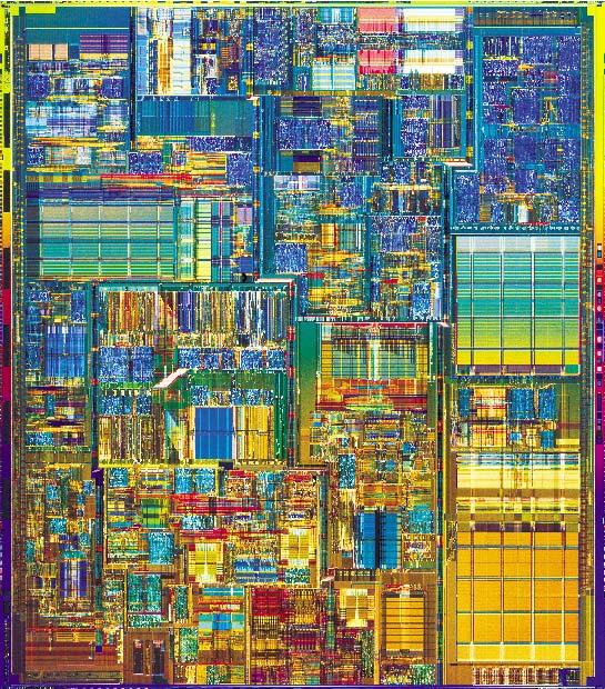
15 Pentium 4 Processor

16 Modern transistors are few microns wide and approximately. micron or less in length Human hair is 8-9 microns in diameter Ref:
17 Transistor Types Bipolar transistors npn or pnp silicon structure Small current into very thin base layer controls large currents between emitter and collector Base currents limit integration density Metal Oxide Semiconductor Field Effect Transistors nmos and pmos MOSFETS Voltage applied to insulated gate controls current between source and drain Low power allows very high integration First patent in the 2s in USA and Germany Not widely used until the 6s or 7s
18 MOS Transistors Four terminal device: gate, source, drain, body Gate oxide body stack looks like a capacitor Gate and body are conductors (body is also called the substrate) SiO 2 (oxide) is a good insulator (separates the gate from the body Called metal oxide semiconductor (MOS) capacitor, even though gate is mostly made of poly-crystalline silicon (polysilicon) Source Gate Drain Polysilicon Polysilicon Source Gate Drain SiO 2 SiO 2 n+ n+ p+ p+ p bulk Si n bulk Si NMOS PMOS
19 NMOS Operation Body is commonly tied to ground ( V) Drain is at a higher voltage than Source When the gate is at a low voltage: P-type body is at low voltage Source-body and drain-body diodes are OFF No current flows, transistor is OFF Source Gate Drain Polysilicon SiO 2 n+ p n+ bulk Si S D
20 NMOS Operation Cont. When the gate is at a high voltage: Positive charge on gate of MOS capacitor Negative charge is attracted to body under the gate Inverts a channel under gate to n-type (N-channel, hence called the NMOS) if the gate voltage is above a threshold voltage (VT) Now current can flow through n-type silicon from source through channel to drain, transistor is ON Source Gate Drain Polysilicon SiO 2 n+ p n+ bulk Si S D
21 PMOS Transistor Similar, but doping and voltages reversed Body tied to high voltage (V DD ) Drain is at a lower voltage than the Source Gate low: transistor ON Gate high: transistor OFF Bubble indicates inverted behavior Polysilicon Source Gate Drain SiO 2 p+ p+ n bulk Si
22 Power Supply Voltage GND = V In 98 s, V DD = 5V V DD has decreased in modern processes High V DD would damage modern tiny transistors Lower V DD saves power V DD = 3.3, 2.5,.8,.5,.2,., Effective power supply voltage can be lower due to IR drop across the power grid.
23 Transistors as Switches In Digital circuits, MOS transistors are electrically controlled switches Voltage at gate controls path from source to g = g = drain nmos g d s d s OFF d s ON pmos g d s d s ON d s OFF
24 CMOS Inverter A Y V DD A Y A Y GND
25 CMOS Inverter A Y V DD OFF A= Y= A Y ON GND Y is pulled low by the turned on NMOS Device. Hence NMOS is the pulldown device.
26 CMOS Inverter A Y V DD ON Y is pulled high by the turned on PMOS Device. Hence PMOS is the pull-up device. A= Y= A Y OFF GND
27 CMOS NAND Gate A B Y Y A B
28 CMOS NAND Gate A B Y A= ON ON Y= OFF B= OFF
29 CMOS NAND Gate A B Y A= OFF ON Y= OFF B= ON
30 CMOS NAND Gate A B Y A= ON OFF Y= ON B= OFF
31 CMOS NAND Gate A B Y A= OFF OFF Y= ON B= ON
32 CMOS NOR Gate A B Y A B Y
33 3-input NAND Gate Y is pulled low if ALL inputs are Y is pulled high if ANY input is A Y B C
34 CMOS Fabrication CMOS transistors are fabricated on silicon wafer Wafers diameters (2-3 mm) Lithography process similar to printing press On each step, different materials are deposited, or patterned or etched Easiest to understand by viewing both top and cross-section of wafer in a simplified manufacturing process
35 Inverter Cross-section Typically use p-type substrate for nmos transistors Requires to make an n-well for body of pmos transistors GND Y A V DD SiO 2 n+ diffusion n+ n+ p+ p substrate n well p+ p+ diffusion polysilicon metal nmos transistor pmos transistor
36 Well and Substrate Taps Substrate must be tied to GND and n-well to V DD Metal to lightly-doped semiconductor forms poor connection called Schottky Diode Use heavily doped well and substrate contacts/taps (or ties) A GND Y V DD p+ n+ n+ p+ p+ n+ p substrate n well substrate tap well tap
37 Inverter Mask Set Top view Transistors and wires are defined by masks Cross-section taken along dashed line A Y GND V DD substrate tap nmos transistor pmos transistor well tap
38 Detailed Mask Views Six masks n-well Polysilicon n+ diffusion p+ diffusion Contact Metal n well Polysilicon n+ Diffusion p+ Diffusion Contact In In reality >4 masks may be needed Metal
39 Fabrication Steps Start with blank wafer (typically p-type where NMOS is created) Build inverter from the bottom up First step will be to form the n-well (where PMOS would reside) Cover wafer with protective layer of SiO 2 (oxide) Remove oxide layer where n-well should be built Implant or diffuse n dopants into exposed wafer to form n-well Strip off SiO 2
40 Oxidation Grow SiO 2 on top of Si wafer 9 2 C with H 2 O or O 2 in oxidation furnace SiO 2 p substrate
41 Photoresist Spin on photoresist Photoresist is a light-sensitive organic polymer Property changes where exposed to light Two types of photoresists (positive or negative) Positive resists can be removed if exposed to UV light Negative resists cannot be removed if exposed to UV light _ Photoresist SiO 2 p substrate
42 Lithography Expose photoresist to Ultra-violate (UV) light through the n-well mask Strip off exposed photoresist with chemicals Photoresist SiO 2 p substrate
43 Etch Etch oxide with hydrofluoric acid (HF) Seeps through skin and eats bone; nasty stuff!!! Only attacks oxide where resist has been exposed N-well pattern is transferred from the mask to silicon-di-oxide surface; creates an opening to the silicon surface Photoresist SiO 2 p substrate
44 Strip Photoresist Strip off remaining photoresist Use mixture of acids called piranah etch Necessary so resist doesn t melt in next step SiO 2 p substrate
45 n-well n-well is formed with diffusion or ion implantation Diffusion Place wafer in furnace with arsenic-rich gas Heat until As atoms diffuse into exposed Si Ion Implanatation Blast wafer with beam of As ions Ions blocked by SiO 2, only enter exposed Si SiO 2 shields (or masks) areas which remain p-type SiO 2 n well
46 Strip Oxide Strip off the remaining oxide using HF Back to bare wafer with n-well Subsequent steps involve similar series of steps p substrate n well
47 Polysilicon (self-aligned gate technology) Deposit very thin layer of gate oxide < 2 Å (6-7 atomic layers) Chemical Vapor Deposition (CVD) of silicon layer Place wafer in furnace with Silane gas (SiH 4 ) Forms many small crystals called polysilicon Heavily doped to be good conductor Polysilicon Thin gate oxide p substrate n well
48 Polysilicon Patterning Use same lithography process discussed earlier to pattern polysilicon Polysilicon Polysilicon Thin gate oxide p substrate n well
49 Self-Aligned Process Use gate-oxide/polysilicon and masking to expose where n+ dopants should be diffused or implanted N-diffusion forms nmos source, drain, and n- well contact p substrate n well
50 N-diffusion/implantation Pattern oxide and form n+ regions Self-aligned process where gate blocks n-dopants Polysilicon is better than metal for self-aligned gates because it doesn t melt during later processing n+ Diffusion p substrate n well
51 N-diffusion/implantation cont. Historically dopants were diffused Usually high energy ion-implantation used today But n+ regions are still called diffusion n+ n+ n+ p substrate n well
52 N-diffusion cont. Strip off oxide to complete patterning step n+ n+ n+ p substrate n well
53 P-Diffusion/implantation Similar set of steps form p+ diffusion regions for PMOS source and drain and substrate contact p+ Diffusion p+ n+ n+ p+ p+ n+ p substrate n well
54 Contacts Now we need to wire together the devices Cover chip with thick field oxide (FO) Etch oxide where contact cuts are needed Contact p+ n+ n+ p+ p+ n+ Thick field oxide p substrate n well
55 Metalization Sputter on aluminum over whole wafer Copper is used in newer technology Pattern to remove excess metal, leaving wires Metal p+ n+ n+ p+ p+ n+ Metal Thick field oxide p substrate n well
56 Physical Layout Chips are specified with set of masks Minimum dimensions of masks determine transistor size (and hence speed, cost, and power) Feature size f = distance between source and drain Set by minimum width of polysilicon Feature size improves 3% every 3 years or so Normalize for feature size when describing design rules Express rules in terms of λ = f/2 E.g. λ =.3 μm in.6 μm process

57 Simplified Design Rules Conservative rules to get you started
,.")
58 Inverter Layout Transistor dimensions specified as Width / Length Minimum size is 4-6λ/ 2λ, sometimes called unit In f =.25 μm process, this is μm wide (W),.25 μm long (L) Since λ=f/2, λ=.25 μm.
59 The Future? International Technology Roadmap for Semiconductors

60
61
62 Summary MOS Transistors are stack of gate, oxide, silicon and p-n junctions Can be viewed as electrically controlled switches Build logic gates out of switches Draw masks to specify layout of transistors Now you know everything necessary to start designing schematics and layout for a simple chip!
VLSI Design. Introduction
 Tassadaq Hussain VLSI Design Introduction Outcome of this course Problem Aims Objectives Outcomes Data Collection Theoretical Model Mathematical Model Validate Development Analysis and Observation Pseudo
420 Intro to VLSI Design
 Dept of Electrical and Computer Engineering 420 Intro to VLSI Design Lecture 0: Course Introduction and Overview Valencia M. Joyner Spring 2005 Getting Started Syllabus About the Instructor Labs, Problem
Lecture 0: Introduction
 Lecture 0: Introduction Introduction Integrated circuits: many transistors on one chip. Very Large Scale Integration (VLSI): bucketloads! Complementary Metal Oxide Semiconductor Fast, cheap, low power
+1 (479)
") Introduction to VLSI Design http://csce.uark.edu +1 (479) 575-6043 yrpeng@uark.edu Invention of the Transistor Vacuum tubes ruled in first half of 20th century Large, expensive, power-hungry, unreliable
Introduction to VLSI Design http://csce.uark.edu +1 (479) 575-6043 yrpeng@uark.edu Invention of the Transistor Vacuum tubes ruled in first half of 20th century Large, expensive, power-hungry, unreliable
FABRICATION OF CMOS INTEGRATED CIRCUITS. Dr. Mohammed M. Farag
 FABRICATION OF CMOS INTEGRATED CIRCUITS Dr. Mohammed M. Farag Outline Overview of CMOS Fabrication Processes The CMOS Fabrication Process Flow Design Rules Reference: Uyemura, John P. "Introduction to
EE4800 CMOS Digital IC Design & Analysis. Lecture 1 Introduction Zhuo Feng
 EE4800 CMOS Digital IC Design & Analysis Lecture 1 Introduction Zhuo Feng 1.1 Prof. Zhuo Feng Office: EERC 730 Phone: 487-3116 Email: zhuofeng@mtu.edu Class Website http://www.ece.mtu.edu/~zhuofeng/ee4800fall2010.html
EMT 251 Introduction to IC Design
 EMT 251 Introduction to IC Design (Pengantar Rekabentuk Litar Terkamir) Semester II 2011/2012 Introduction to IC design and Transistor Fundamental Some Keywords! Very-large-scale-integration (VLSI) is
Basic Fabrication Steps
 Basic Fabrication Steps and Layout Somayyeh Koohi Department of Computer Engineering Adapted with modifications from lecture notes prepared by author Outline Fabrication steps Transistor structures Transistor
Topic 3. CMOS Fabrication Process
 Topic 3 CMOS Fabrication Process Peter Cheung Department of Electrical & Electronic Engineering Imperial College London URL: www.ee.ic.ac.uk/pcheung/ E-mail: p.cheung@ic.ac.uk Lecture 3-1 Layout of a Inverter
Transistor was first invented by William.B.Shockley, Walter Brattain and John Bardeen of Bell Labratories. In 1961, first IC was introduced.
 Unit 1 Basic MOS Technology Transistor was first invented by William.B.Shockley, Walter Brattain and John Bardeen of Bell Labratories. In 1961, first IC was introduced. Levels of Integration:- i) SSI:-
Layout of a Inverter. Topic 3. CMOS Fabrication Process. The CMOS Process - photolithography (2) The CMOS Process - photolithography (1) v o.
 The CMOS Process - photolithography (1) v o.") Layout of a Inverter Topic 3 CMOS Fabrication Process V DD Q p Peter Cheung Department of Electrical & Electronic Engineering Imperial College London v i v o Q n URL: www.ee.ic.ac.uk/pcheung/ E-mail: p.cheung@ic.ac.uk
Layout of a Inverter Topic 3 CMOS Fabrication Process V DD Q p Peter Cheung Department of Electrical & Electronic Engineering Imperial College London v i v o Q n URL: www.ee.ic.ac.uk/pcheung/ E-mail: p.cheung@ic.ac.uk
Spiral 1 / Unit 8. Transistor Implementations CMOS Logic Gates
 18.1 Spiral 1 / Unit 8 Transistor Implementations CMOS Logic Gates 18.2 Spiral Content Mapping Spiral Theory Combinational Design Sequential Design System Level Design Implementation and Tools Project
Outcomes. Spiral 1 / Unit 8. DeMorgan s Theorem DEMORGAN'S THEOREM. Transistor Implementations CMOS Logic Gates
 18.1 18.2 Spiral 1 / Unit 8 Transistor Implementations MOS Logic Gates Mark Redekopp Outcomes I know the difference between combinational and sequential logic and can name examples of each. I understand
CMOS Digital Integrated Circuits Lec 2 Fabrication of MOSFETs
 CMOS Digital Integrated Circuits Lec 2 Fabrication of MOSFETs 1 CMOS Digital Integrated Circuits 3 rd Edition Categories of Materials Materials can be categorized into three main groups regarding their
Chapter 1, Introduction
 Introduction to Semiconductor Manufacturing Technology Chapter 1, Introduction hxiao89@hotmail.com 1 Objective After taking this course, you will able to Use common semiconductor terminology Describe a
Lecture 0: Introduction
 Introduction to CMOS VLSI Design Lecture : Introduction David Harris Steven Levitan Harvey Mudd College University of Pittsburgh Spring 24 Fall 28 Administrivia Professor Steven Levitan TA: Bo Zhao Syllabus
INTRODUCTION TO MOS TECHNOLOGY
 INTRODUCTION TO MOS TECHNOLOGY 1. The MOS transistor The most basic element in the design of a large scale integrated circuit is the transistor. For the processes we will discuss, the type of transistor
EE 5611 Introduction to Microelectronic Technologies Fall Thursday, September 04, 2014 Lecture 02
 EE 5611 Introduction to Microelectronic Technologies Fall 2014 Thursday, September 04, 2014 Lecture 02 1 Lecture Outline Review on semiconductor materials Review on microelectronic devices Example of microelectronic
EE 330 Lecture 7. Design Rules. IC Fabrication Technology Part 1
 EE 330 Lecture 7 Design Rules IC Fabrication Technology Part 1 Review from Last Time Technology Files Provide Information About Process Process Flow (Fabrication Technology) Model Parameters Design Rules
Chapter 3: Basics Semiconductor Devices and Processing 2006/9/27 1. Topics
 Chapter 3: Basics Semiconductor Devices and Processing 2006/9/27 1 Topics What is semiconductor Basic semiconductor devices Basics of IC processing CMOS technologies 2006/9/27 2 1 What is Semiconductor
Chapter 3 Basics Semiconductor Devices and Processing
 Chapter 3 Basics Semiconductor Devices and Processing 1 Objectives Identify at least two semiconductor materials from the periodic table of elements List n-type and p-type dopants Describe a diode and
Introduction to VLSI ASIC Design and Technology
 Introduction to VLSI ASIC Design and Technology Paulo Moreira CERN - Geneva, Switzerland Paulo Moreira Introduction 1 Outline Introduction Is there a limit? Transistors CMOS building blocks Parasitics
Lecture Integrated circuits era
 Lecture 1 1.1 Integrated circuits era Transistor was first invented by William.B.Shockley, Walter Brattain and John Bardeen of Bell laboratories. In 1961, first IC was introduced. Levels of Integration:-
ECE 5745 Complex Digital ASIC Design Topic 2: CMOS Devices
 ECE 5745 Complex Digital ASIC Design Topic 2: CMOS Devices Christopher Batten School of Electrical and Computer Engineering Cornell University http://www.csl.cornell.edu/courses/ece5950 Simple Transistor
Notes. (Subject Code: 7EC5)
") COMPUCOM INSTITUTE OF TECHNOLOGY & MANAGEMENT, JAIPUR (DEPARTMENT OF ELECTRONICS & COMMUNICATION) Notes VLSI DESIGN NOTES (Subject Code: 7EC5) Prepared By: MANVENDRA SINGH Class: B. Tech. IV Year, VII
COMPUCOM INSTITUTE OF TECHNOLOGY & MANAGEMENT, JAIPUR (DEPARTMENT OF ELECTRONICS & COMMUNICATION) Notes VLSI DESIGN NOTES (Subject Code: 7EC5) Prepared By: MANVENDRA SINGH Class: B. Tech. IV Year, VII
ECE 2300 Digital Logic & Computer Organization
 ECE 2300 Digital Logic & Computer Organization Spring 2018 CMOS Logic Lecture 4: 1 NAND Logic Gate X Y (X Y) = NAND Using De Morgan s Law: (X Y) = X +Y X X X +Y = Y Y Also a NAND We can build circuits
Progress due to: Feature size reduction - 0.7X/3 years (Moore s Law). Increasing chip size - 16% per year. Creativity in implementing functions.
. Increasing chip size - 16% per year. Creativity in implementing functions.") Introduction - Chapter 1 Evolution of IC Fabrication 1960 and 1990 integrated t circuits. it Progress due to: Feature size reduction - 0.7X/3 years (Moore s Law). Increasing chip size - 16% per year. Creativity
Introduction - Chapter 1 Evolution of IC Fabrication 1960 and 1990 integrated t circuits. it Progress due to: Feature size reduction - 0.7X/3 years (Moore s Law). Increasing chip size - 16% per year. Creativity
2.8 - CMOS TECHNOLOGY
 CMOS Technology (6/7/00) Page 1 2.8 - CMOS TECHNOLOGY INTRODUCTION Objective The objective of this presentation is: 1.) Illustrate the fabrication sequence for a typical MOS transistor 2.) Show the physical
Student Lecture by: Giangiacomo Groppi Joel Cassell Pierre Berthelot September 28 th 2004
 Student Lecture by: Giangiacomo Groppi Joel Cassell Pierre Berthelot September 28 th 2004 Lecture outline Historical introduction Semiconductor devices overview Bipolar Junction Transistor (BJT) Field
Design cycle for MEMS
 Design cycle for MEMS Design cycle for ICs IC Process Selection nmos CMOS BiCMOS ECL for logic for I/O and driver circuit for critical high speed parts of the system The Real Estate of a Wafer MOS Transistor
Integrated Circuit Technology (Course Code: EE662) Lecture 1: Introduction
 Lecture 1: Introduction") Indian Institute of Technology Jodhpur, Year 2015 2016 Integrated Circuit Technology (Course Code: EE662) Lecture 1: Introduction Course Instructor: Shree Prakash Tiwari, Ph.D. Email: sptiwari@iitj.ac.in
Indian Institute of Technology Jodhpur, Year 2015 2016 Integrated Circuit Technology (Course Code: EE662) Lecture 1: Introduction Course Instructor: Shree Prakash Tiwari, Ph.D. Email: sptiwari@iitj.ac.in
MICROPROCESSOR TECHNOLOGY
 MICROPROCESSOR TECHNOLOGY Assis. Prof. Hossam El-Din Moustafa Lecture 3 Ch.1 The Evolution of The Microprocessor 17-Feb-15 1 Chapter Objectives Introduce the microprocessor evolution from transistors to
Semiconductor Physics and Devices
 Metal-Semiconductor and Semiconductor Heterojunctions The Metal-Oxide-Semiconductor Field-Effect Transistor (MOSFET) is one of two major types of transistors. The MOSFET is used in digital circuit, because
Lecture 8. MOS Transistors; Cheap Computers; Everycircuit
 Lecture 8 MOS Transistors; Cheap Computers; Everycircuit Copyright 2017 by Mark Horowitz 1 Reading The rest of Chapter 4 in the reader For more details look at A&L 5.1 Digital Signals (goes in much more
APPLICATION TRAINING GUIDE
 APPLICATION TRAINING GUIDE Basic Semiconductor Theory Semiconductor is an appropriate name for the device because it perfectly describes the material from which it's made -- not quite a conductor, and
Integrated diodes. The forward voltage drop only slightly depends on the forward current. ELEKTRONIKOS ĮTAISAI
 1 Integrated diodes pn junctions of transistor structures can be used as integrated diodes. The choice of the junction is limited by the considerations of switching speed and breakdown voltage. The forward
Advantage of Having Large Numbers of Function on a Single Chip. Less Area occupied Less power Consumption Higher Speed Higher Reliability Economical
 VLSI DESIGN(UNIT 1) Introduction Some History Invention of the transistor (BJT) 1947 Single-transistor integrated circuit 1958 Invention of CMOS logic gates 1963 First microprocessor (Intel 4004)1970 Very
EECS 151/251A Spring 2019 Digital Design and Integrated Circuits. Instructors: Wawrzynek. Lecture 8 EE141
 EECS 151/251A Spring 2019 Digital Design and Integrated Circuits Instructors: Wawrzynek Lecture 8 EE141 From the Bottom Up IC processing CMOS Circuits (next lecture) EE141 2 Overview of Physical Implementations
Layers. Layers. Layers. Transistor Manufacturing COMP375 1
 Layers VLSI COMP370 Intro to Computer Architecture t Applications Middleware other CS classes High level languages Machine Language Microcode Logic circuits Gates Transistors Silicon structures Layers
Introduction. Reading: Chapter 1. Courtesy of Dr. Dansereau, Dr. Brown, Dr. Vranesic, Dr. Harris, and Dr. Choi.
 Introduction Reading: Chapter 1 Courtesy of Dr. Dansereau, Dr. Brown, Dr. Vranesic, Dr. Harris, and Dr. Choi http://csce.uark.edu +1 (479) 575-6043 yrpeng@uark.edu Why study logic design? Obvious reasons
Layers. Layers. Layers. Transistor Manufacturing COMP375 1
 VLSI COMP375 Computer Architecture Middleware other CS classes Machine Language Microcode Logic circuits Transistors Middleware Machine Language - earlier Microcode Logic circuits Transistors Middleware
In this lecture we will begin a new topic namely the Metal-Oxide-Semiconductor Field Effect Transistor.
 Solid State Devices Dr. S. Karmalkar Department of Electronics and Communication Engineering Indian Institute of Technology, Madras Lecture - 38 MOS Field Effect Transistor In this lecture we will begin
Microelectronics, BSc course
 Microelectronics, BSc course MOS circuits: CMOS circuits, construction http://www.eet.bme.hu/~poppe/miel/en/14-cmos.pptx http://www.eet.bme.hu The abstraction level of our study: SYSTEM + MODULE GATE CIRCUIT
Chapter 2 : Semiconductor Materials & Devices (II) Feb
 Feb") Chapter 2 : Semiconductor Materials & Devices (II) 1 Reference 1. SemiconductorManufacturing Technology: Michael Quirk and Julian Serda (2001) 3. Microelectronic Circuits (5/e): Sedra & Smith (2004) 4.
Chapter 2 : Semiconductor Materials & Devices (II) 1 Reference 1. SemiconductorManufacturing Technology: Michael Quirk and Julian Serda (2001) 3. Microelectronic Circuits (5/e): Sedra & Smith (2004) 4.
ECE520 VLSI Design. Lecture 2: Basic MOS Physics. Payman Zarkesh-Ha
 ECE520 VLSI Design Lecture 2: Basic MOS Physics Payman Zarkesh-Ha Office: ECE Bldg. 230B Office hours: Wednesday 2:00-3:00PM or by appointment E-mail: pzarkesh@unm.edu Slide: 1 Review of Last Lecture Semiconductor
Basic Electronics. Introductory Lecture Course for. Technology and Instrumentation in Particle Physics Chicago, Illinois June 9-14, 2011
 Basic Electronics Introductory Lecture Course for Technology and Instrumentation in Particle Physics 2011 Chicago, Illinois June 9-14, 2011 Presented By Gary Drake Argonne National Laboratory Session 3
2009 Spring CS211 Digital Systems & Lab 1 CHAPTER 3: TECHNOLOGY (PART 2)
") 1 CHAPTER 3: IMPLEMENTATION TECHNOLOGY (PART 2) Whatwillwelearninthischapter? we learn in this 2 How transistors operate and form simple switches CMOS logic gates IC technology FPGAs and other PLDs Basic
1 CHAPTER 3: IMPLEMENTATION TECHNOLOGY (PART 2) Whatwillwelearninthischapter? we learn in this 2 How transistors operate and form simple switches CMOS logic gates IC technology FPGAs and other PLDs Basic
Mathematics and Science in Schools in Sub-Saharan Africa
 Mathematics and Science in Schools in Sub-Saharan Africa SEMICONDUCTORS What is a Semiconductor? What is a Semiconductor? Microprocessors LED Transistors Capacitors Range of Conduciveness The semiconductors
Spiral Content Mapping. Spiral 1 / Unit 8. Outcomes DEMORGAN'S THEOREM. Transistor Implementations CMOS Logic Gates
 18.1 18.2 Spiral ontent Mapping Spiral Theory ombinational esign Sequential esign System Level esign Implementation and Tools Project Spiral 1 / Unit 8 Transistor Implementations MOS Logic Gates Performance
EE301 Electronics I , Fall
 EE301 Electronics I 2018-2019, Fall 1. Introduction to Microelectronics (1 Week/3 Hrs.) Introduction, Historical Background, Basic Consepts 2. Rewiev of Semiconductors (1 Week/3 Hrs.) Semiconductor materials
TECHNO INDIA BATANAGAR (DEPARTMENT OF ELECTRONICS & COMMUNICATION ENGINEERING) QUESTION BANK- 2018
 QUESTION BANK- 2018") TECHNO INDIA BATANAGAR (DEPARTMENT OF ELECTRONICS & COMMUNICATION ENGINEERING) QUESTION BANK- 2018 Paper Setter Detail Name Designation Mobile No. E-mail ID Raina Modak Assistant Professor 6290025725 raina.modak@tib.edu.in
TECHNO INDIA BATANAGAR (DEPARTMENT OF ELECTRONICS & COMMUNICATION ENGINEERING) QUESTION BANK- 2018 Paper Setter Detail Name Designation Mobile No. E-mail ID Raina Modak Assistant Professor 6290025725 raina.modak@tib.edu.in
Device Technologies. Yau - 1
 Device Technologies Yau - 1 Objectives After studying the material in this chapter, you will be able to: 1. Identify differences between analog and digital devices and passive and active components. Explain
EC0306 INTRODUCTION TO VLSI DESIGN
 EC0306 INTRODUCTION TO VLSI DESIGN UNIT I INTRODUCTION TO MOS CIRCUITS Why VLSI? Integration improves the design: o lower parasitics = higher speed; o lower power; o physically smaller. Integration reduces
Lecture 1 Introduction to Solid State Electronics
 EE 471: Transport Phenomena in Solid State Devices Spring 2018 Lecture 1 Introduction to Solid State Electronics Bryan Ackland Department of Electrical and Computer Engineering Stevens Institute of Technology
Semiconductor Devices
 Semiconductor Devices - 2014 Lecture Course Part of SS Module PY4P03 Dr. P. Stamenov School of Physics and CRANN, Trinity College, Dublin 2, Ireland Hilary Term, TCD 3 th of Feb 14 MOSFET Unmodified Channel
ENG2410 Digital Design CMOS Technology. Fall 2017 S. Areibi School of Engineering University of Guelph
 ENG2410 Digital Design CMOS Technology Fall 2017 S. reibi School of Engineering University of Guelph The Transistor Revolution First transistor Bell Labs, 1948 Bipolar logic 1960 s Intel 4004 processor
College of Engineering Department of Electrical Engineering and Computer Sciences University of California, Berkeley
 College of Engineering Department of Electrical Engineering and Below are your weekly quizzes. You should print out a copy of the quiz and complete it before your lab section. Bring in the completed quiz
1 FUNDAMENTAL CONCEPTS What is Noise Coupling 1
 Contents 1 FUNDAMENTAL CONCEPTS 1 1.1 What is Noise Coupling 1 1.2 Resistance 3 1.2.1 Resistivity and Resistance 3 1.2.2 Wire Resistance 4 1.2.3 Sheet Resistance 5 1.2.4 Skin Effect 6 1.2.5 Resistance
Laboratory #5 BJT Basics and MOSFET Basics
 Laboratory #5 BJT Basics and MOSFET Basics I. Objectives 1. Understand the physical structure of BJTs and MOSFETs. 2. Learn to measure I-V characteristics of BJTs and MOSFETs. II. Components and Instruments
EECS130 Integrated Circuit Devices
 EECS130 Integrated Circuit Devices Professor Ali Javey 11/6/2007 MOSFETs Lecture 6 BJTs- Lecture 1 Reading Assignment: Chapter 10 More Scalable Device Structures Vertical Scaling is important. For example,
Shorthand Notation for NMOS and PMOS Transistors
 Shorthand Notation for NMOS and PMOS Transistors Terminal Voltages Mode of operation depends on V g, V d, V s V gs = V g V s V gd = V g V d V ds = V d V s = V gs - V gd Source and drain are symmetric diffusion
Session 3: Solid State Devices. Silicon on Insulator
 Session 3: Solid State Devices Silicon on Insulator 1 Outline A B C D E F G H I J 2 Outline Ref: Taurand Ning 3 SOI Technology SOl materials: SIMOX, BESOl, and Smart Cut SIMOX : Synthesis by IMplanted
Lecture 020 ECE4430 Review II (1/5/04) Page 020-1
 Page 020-1") Lecture 020 ECE4430 Review II (1/5/04) Page 020-1 LECTURE 020 ECE 4430 REVIEW II (READING: GHLM - Chap. 2) Objective The objective of this presentation is: 1.) Identify the prerequisite material as taught
Lecture 020 ECE4430 Review II (1/5/04) Page 020-1 LECTURE 020 ECE 4430 REVIEW II (READING: GHLM - Chap. 2) Objective The objective of this presentation is: 1.) Identify the prerequisite material as taught
Homework 10 posted just for practice. Office hours next week, schedule TBD. HKN review today. Your feedback is important!
 EE141 Fall 2005 Lecture 26 Memory (Cont.) Perspectives Administrative Stuff Homework 10 posted just for practice No need to turn in Office hours next week, schedule TBD. HKN review today. Your feedback
Introduction to Electronic Devices
 (Course Number 300331) Fall 2006 Instructor: Dr. Dietmar Knipp Assistant Professor of Electrical Engineering Information: http://www.faculty.iubremen.de/dknipp/ Source: Apple Ref.: Apple Ref.: IBM Critical
Module-3: Metal Oxide Semiconductor (MOS) & Emitter coupled logic (ECL) families
 & Emitter coupled logic (ECL) families") 1 Module-3: Metal Oxide Semiconductor (MOS) & Emitter coupled logic (ECL) families 1. Introduction 2. Metal Oxide Semiconductor (MOS) logic 2.1. Enhancement and depletion mode 2.2. NMOS and PMOS inverter
1 Module-3: Metal Oxide Semiconductor (MOS) & Emitter coupled logic (ECL) families 1. Introduction 2. Metal Oxide Semiconductor (MOS) logic 2.1. Enhancement and depletion mode 2.2. NMOS and PMOS inverter
VLSI Technology Dr. Nandita Dasgupta Department of Electrical Engineering Indian Institute of Technology, Madras
 VLSI Technology Dr. Nandita Dasgupta Department of Electrical Engineering Indian Institute of Technology, Madras Lecture - 39 Latch up in CMOS We have been discussing about the problems in CMOS, basic
ATV 2011: Computer Engineering
 ATV 2011: Technology Trends in Computer Engineering Professor Per Larsson-Edefors ATV 2011, L1, Per Larsson-Edefors Page 1 Solid-State Devices www.cse.chalmers.se/~perla/ugrad/ SemTech/Lectures_2000.pdf
Digital Integrated Circuits
 Digital Integrated Circuits Yaping Dan ( 但亚平 ), PhD Office: Law School North 301 Tel: 34206045-3011 Email: yapingd@gmail.com Digital Integrated Circuits Introduction p-n junctions and MOSFETs The CMOS
CMOS Technology. 1. Why CMOS 2. Qualitative MOSFET model 3. Building a MOSFET 4. CMOS logic gates. Handouts: Lecture Slides. metal ndiff.
 CMOS Technology 1. Why CMOS 2. Qualitative MOSFET model 3. Building a MOSFET 4. CMOS logic gates poly pdiff metal ndiff Handouts: Lecture Slides L03 - CMOS Technology 1 Building Bits from Atoms V in V
Architecture of Computers and Parallel Systems Part 9: Digital Circuits
 Architecture of Computers and Parallel Systems Part 9: Digital Circuits Ing. Petr Olivka petr.olivka@vsb.cz Department of Computer Science FEI VSB-TUO Architecture of Computers and Parallel Systems Part
Jack Keil Wolf Lecture. ESE 570: Digital Integrated Circuits and VLSI Fundamentals. Lecture Outline. MOSFET N-Type, P-Type.
 ESE 570: Digital Integrated Circuits and VLSI Fundamentals Jack Keil Wolf Lecture Lec 3: January 24, 2019 MOS Fabrication pt. 2: Design Rules and Layout http://www.ese.upenn.edu/about-ese/events/wolf.php
Learning Outcomes. Spiral 2-6. Current, Voltage, & Resistors DIODES
 26.1 26.2 Learning Outcomes Spiral 26 Semiconductor Material MOS Theory I underst why a diode conducts current under forward bias but does not under reverse bias I underst the three modes of operation
VLSI: An Introduction
 Chapter 1 UEEA2223/UEEG4223 Integrated Circuit Design VLSI: An Introduction Prepared by Dr. Lim Soo King 02 Jan 2011. Chapter 1 VLSI Design: An Introduction... 1 1.0 Introduction... 1 1.0.1 Early Computing
FUNDAMENTALS OF MODERN VLSI DEVICES
 19-13- FUNDAMENTALS OF MODERN VLSI DEVICES YUAN TAUR TAK H. MING CAMBRIDGE UNIVERSITY PRESS Physical Constants and Unit Conversions List of Symbols Preface page xi xiii xxi 1 INTRODUCTION I 1.1 Evolution
Semiconductor Physics and Devices
 Nonideal Effect The experimental characteristics of MOSFETs deviate to some degree from the ideal relations that have been theoretically derived. Semiconductor Physics and Devices Chapter 11. MOSFET: Additional
Solid State Devices- Part- II. Module- IV
 Solid State Devices- Part- II Module- IV MOS Capacitor Two terminal MOS device MOS = Metal- Oxide- Semiconductor MOS capacitor - the heart of the MOSFET The MOS capacitor is used to induce charge at the
LSI ON GLASS SUBSTRATES
 LSI ON GLASS SUBSTRATES OUTLINE Introduction: Why System on Glass? MOSFET Technology Low-Temperature Poly-Si TFT Technology System-on-Glass Technology Issues Conclusion System on Glass CPU SRAM DRAM EEPROM
Unit-1. MOS Transistor Theory
 VLSI DESIGN -EEE Unit-1 MOS Transistor Theory VLSI DESIGN UNIT I Contents: 1.1 Historical Perspective 1.2 What is VLSI? - Introduction 1.3 VLSI Design Flow 1.4 Design Hierarchy 1.5 Basic MOS Transistor
Introduction to Materials Engineering: Materials Driving the Electronics Revolution Robert Hull, MSE
 Introduction to Materials Engineering: Materials Driving the Electronics Revolution Robert Hull, MSE Outline Microelectronics Miniaturization Historical Development: Electronics before Semiconductors The
PAPER SOLUTION_DECEMBER_2014_VLSI_DESIGN_ETRX_SEM_VII Prepared by Girish Gidaye
 Q1a) The MOS System under External Bias Depending on the polarity and the magnitude of V G, three different operating regions can be observed for the MOS system: 1) Accumulation 2) Depletion 3) Inversion
Semiconductor Diodes
 Semiconductor Diodes A) Motivation and Game Plan B) Semiconductor Doping and Conduction C) Diode Structure and I vs. V D) Diode Circuits Reading: Schwarz and Oldham, Chapter 13.1-13.2 Motivation Digital
Logic Design (Part 1) Transistors & Gates (Chapter 3)
 Transistors & Gates (Chapter 3)") Agenda next 3 weeks: Inside a microprocessor Logic Design (Part 1) Transistors & Gates (Chapter 3) Based on slides McGrawHill Additional material 2004/2005/2006 Lewis/Martin Additional material 2008 Roth
Agenda next 3 weeks: Inside a microprocessor Logic Design (Part 1) Transistors & Gates (Chapter 3) Based on slides McGrawHill Additional material 2004/2005/2006 Lewis/Martin Additional material 2008 Roth
Silicon VLSI Technology. Fundamentals, Practice and Modeling. Class Notes For Instructors. J. D. Plummer, M. D. Deal and P. B.
 Silicon VLSI Technology Fundamentals, ractice, and Modeling Class otes For Instructors J. D. lummer, M. D. Deal and. B. Griffin These notes are intended to be used for lectures based on the above text.
UNIT-1 Bipolar Junction Transistors. Text Book:, Microelectronic Circuits 6 ed., by Sedra and Smith, Oxford Press
 UNIT-1 Bipolar Junction Transistors Text Book:, Microelectronic Circuits 6 ed., by Sedra and Smith, Oxford Press Figure 6.1 A simplified structure of the npn transistor. Microelectronic Circuits, Sixth
Lecture #29. Moore s Law
 Lecture #29 ANNOUNCEMENTS HW#15 will be for extra credit Quiz #6 (Thursday 5/8) will include MOSFET C-V No late Projects will be accepted after Thursday 5/8 The last Coffee Hour will be held this Thursday
UNIT-VI FIELD EFFECT TRANSISTOR. 1. Explain about the Field Effect Transistor and also mention types of FET s.
 UNIT-I FIELD EFFECT TRANSISTOR 1. Explain about the Field Effect Transistor and also mention types of FET s. The Field Effect Transistor, or simply FET however, uses the voltage that is applied to their
Lesson 5. Electronics: Semiconductors Doping p-n Junction Diode Half Wave and Full Wave Rectification Introduction to Transistors-
 Lesson 5 Electronics: Semiconductors Doping p-n Junction Diode Half Wave and Full Wave Rectification Introduction to Transistors- Types and Connections Semiconductors Semiconductors If there are many free
Power Bipolar Junction Transistors (BJTs)
") ECE442 Power Semiconductor Devices and Integrated Circuits Power Bipolar Junction Transistors (BJTs) Zheng Yang (ERF 3017, email: yangzhen@uic.edu) Power Bipolar Junction Transistor (BJT) Background The
ECE442 Power Semiconductor Devices and Integrated Circuits Power Bipolar Junction Transistors (BJTs) Zheng Yang (ERF 3017, email: yangzhen@uic.edu) Power Bipolar Junction Transistor (BJT) Background The
PHYSICAL STRUCTURE OF CMOS INTEGRATED CIRCUITS. Dr. Mohammed M. Farag
 PHYSICAL STRUCTURE OF CMOS INTEGRATED CIRCUITS Dr. Mohammed M. Farag Outline Integrated Circuit Layers MOSFETs CMOS Layers Designing FET Arrays EE 432 VLSI Modeling and Design 2 Integrated Circuit Layers
UNIT III VLSI CIRCUIT DESIGN PROCESSES. In this chapter we will be studying how to get the schematic into stick diagrams or layouts.
 UNIT III VLSI CIRCUIT DESIGN PROCESSES In this chapter we will be studying how to get the schematic into stick diagrams or layouts. MOS circuits are formed on four basic layers: N-diffusion P-diffusion
Power Semiconductor Devices
 TRADEMARK OF INNOVATION Power Semiconductor Devices Introduction This technical article is dedicated to the review of the following power electronics devices which act as solid-state switches in the circuits.
Introduction to VLSI Technology
 Introduction to VLSI Technology Introduction: The invention of the transistor by William B. Shockley, Walter H. Brattain and John Bardeen of Bell Telephone Laboratories drastically changed the electronics
ESE 570: Digital Integrated Circuits and VLSI Fundamentals
 ESE 570: Digital Integrated Circuits and VLSI Fundamentals Lec 3: January 24, 2019 MOS Fabrication pt. 2: Design Rules and Layout Penn ESE 570 Spring 2019 Khanna Jack Keil Wolf Lecture http://www.ese.upenn.edu/about-ese/events/wolf.php
ECE/CoE 0132: FETs and Gates
 ECE/CoE 0132: FETs and Gates Kartik Mohanram September 6, 2017 1 Physical properties of gates Over the next 2 lectures, we will discuss some of the physical characteristics of integrated circuits. We will
INTRODUCTION A. VACUUM TUBES
 ITRODUCTIO The words, integrated circuits, semiconductor, microprocessor, and memory, are a part of the world we live in today. What is it all about and why is it important to you and me? It's about the
Lecture 4 - Digital Representations III + Transistors
 Lecture 4 - Digital Representations III + Transistors Video: Seems like a natural extension from images no? We just have a new dimension (time) Each frame is just an image made up of pixels Display n frames
BICMOS Technology and Fabrication
 12-1 BICMOS Technology and Fabrication 12-2 Combines Bipolar and CMOS transistors in a single integrated circuit By retaining benefits of bipolar and CMOS, BiCMOS is able to achieve VLSI circuits with
ECE 340 Lecture 37 : Metal- Insulator-Semiconductor FET Class Outline:
 ECE 340 Lecture 37 : Metal- Insulator-Semiconductor FET Class Outline: Metal-Semiconductor Junctions MOSFET Basic Operation MOS Capacitor Things you should know when you leave Key Questions What is the