Semiconductor Memory: DRAM and SRAM. Department of Electrical and Computer Engineering, National University of Singapore
|
|
|
- Sandra Bruce
- 6 years ago
- Views:
Transcription
1 Semiconductor Memory: DRAM and SRAM
2 Outline Introduction Random Access Memory (RAM) DRAM SRAM Non-volatile memory UV EPROM EEPROM Flash memory SONOS memory QD memory
3 Introduction Slow memories Magnetic and optical disk Magnetic tape Slow and high capacity Semiconductor memories DRAM SRAM Non-volatile memory High cost, fast, and use of MOSFET
4 Introduction (2)
5 Introduction (3)
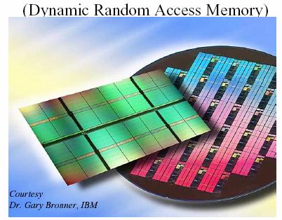
6 DRAM (1) Introduction The highest density semiconductor product Used as the indicator of the technology level Forerunner of the most advanced technology Consist of 1T1C (1 transistor and 1 capacitor) Charge stored in capacitor When capacitor is charged to a high voltage, the DRAM cell stores a 1 state; when C is charged to a low voltage, the DRAM cell stores a 0 state.
7 DRAM (2) Operation principle (I) Write and read operation - Write: When WL is selected, the data stored on BL will be stored in the capacitor -Read: BL is pre-charged to V DD /2, when WL is selected, the potential at X will be higher than V DD /2 or lower than V DD /2 depends on the stored data.

8 DRAM (3) Operation principle (I) Charge sharing sensing -C B /C S (bit line capacitance over memory cell capacitance, normally larger than 10) is one of most important parameter in DRAM design - when read, the potential will be charged. The sense amplifier must be sensitive enough to read this signal - the change of potential in memory cell node can be given as below: - in practice, the minimum voltage detected by the sense amplifier is 100mV. For higher density, the sensitivity of sense amplifier should be much increased.

9 DRAM (4) Operation principle (I) Refresh - The voltage stored on 1 memory cell will slowly decades to a 0 voltage state through various leakage mechanisms - Periodically reading the data and rewriting the same data is necessary which is called refresh. - Leakage mechanisms include - Junction leakage - Pass transistor sub-threshold leakage - Leakage through capacitor dielectrics - Other parasitic leakage paths
10 Operation principle (I) DRAM (5) Soft errors - alpha particle double charged helium nuclei that originates from the decay of radioactive elements in the package or metallization material. only determined by the total amount of charge collected by the cell node. - cosmic rays a very small percentage of high-energy neutrons will interact by colliding with silicon nucleus, which generate charges.
 stacked capacitor DRAM cell (ii) trench capacitor")
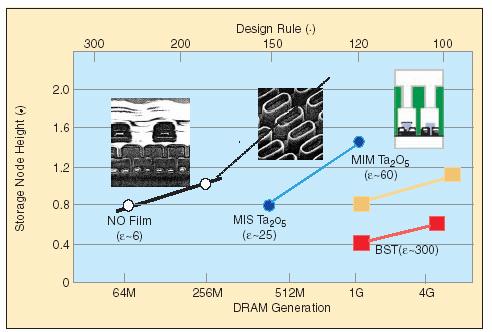
11 DRAM (6) Operation principle (I) Cell scaling Approaches to cell scaling reduce thickness increase dielectric constant increase capacitance area (i) stacked capacitor DRAM cell (ii) trench capacitor DRAM cell
12 DRAM (7) Operation principle (I) Cell scaling Reducing dielectric thickness t - this approach is mainly limited by Fowler-Nordheim tunneling current - primarily constrains in reducing the dielectric thickness originate from dielectric reliability, leakage current, etc. Increasing dielectric constant - O (oxide) ONO (oxide nitride oxide) NO (oxide nitride) Ta2O5 higher dielectric constant material (BST, PZT, etc.) - combination of oxide and nitride can provide at best 4 nm in effective oxide thickness - Ta2O5 film has a higher dielectric constant, and demonstrated with 3 nm effective oxide thickness, but the process feasibility is still not proven yet. - for PZT, BST, a lot of process issues exist.
 and is stacked over the pass transistor.")
13 DRAM (8) Operation principle (I) Cell scaling Increasing area A Stacked capacitor DRAM cell the capacitor dielectric film is formed between the two heavily doped poly-si (or metal) and is stacked over the pass transistor. the device structure is simple process is less sensitive
14 DRAM (9) Operation principle (I) Cell scaling Increasing area A Trench capacitor DRAM cell the capacitor dielectric film is formed inside a trenched etched into the silicon substrate and between two heavily doped silicon layers or metals has advantage in super planarity process is complicated and difficult
15 DRAM (10) Comments Cell scaling New memory architecture and circuit technique to reduce cell size On-chip integration of DRAM and logic circuits (embedded DRAM) Increasing difficult to meet soft-error requirement
16 DRAM (11)
17 1G DRAM
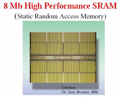
18 SRAM (1) Introduction An SRAM cell is a bistable transistor flip-flop, or two inverters connected back to back. Type of SRAM Depletion load Resistor load Full CMOS TFT load
19 SRAM (2) Example TFT load SRAM cell structure P-channel TFT is fabricated on top of an n+ poly-si gate The n+ poly-si gate is shared with bottom n-channel bulk MOSFET and p-channel TFT The drain of TFT is offset from the gate to reduce the leakage current
20 SRAM (3) Comparison of different SRAM structures Depletion load Use depletion-mode n-mos transistor as load Oldest type before CMOS technology Resistor load Use high-resistance polysilicon resistor as load Small cell area and high density Full CMOS load Use bulk p-mos transistor as load Cell size tend to be larger than R-load cell Very low standby current Currently the dominant technology due to good stability at low power supply TFT load Use p-channel TFT as load Combines the low-power advantages of the full CMOS load cell and the high density advantages of R-load cell Has been popular for a while, but received less attention recently due to poor stability at low power supply and process complexity
21 SRAM (4) Operation principles Write operation (writing 1 as example) - Word line of the cell is selected (raised to VDD, 5V) T5 and T6 turn ON - Bit-bar line must be forced low T1 turns OFF and T3 turns ON - The drain voltage at C5 rises due to the current flowing through T5 and T3 - When T2 has been turned ON, the bit line can be returned to its steady level, leaving the cell in the state of storing a 1.
22 Operation principles SRAM (5) Read operation (reading 1 as example) - The word line of the cell is selected (raised to VDD) T5 and T6 are turned ON. - Both the Bit line and Bit-bar line must be biased at some voltage (for example, 3V) - When the cell is selected, currents flow through T6 and T2 to Vss and through T3 and T5 to the bit line. - Since T2 remaining ON, the voltage of bit-bar line is reduced to less than 3V - While the voltage of bit line is pulled up above 3V since T1 is OFF but T3 is ON - The differential output signal between the bit and bit-bar lines is fed into the sense amplifier, which in SRAMs is a differential amplifier capable of providing rapid sensing.
23 SRAM (6) Cell stability analysis Cell stability determines the soft-error rate and the sensibility of the memory cell to variation in process and operating condition Cell ratio (β ratio) Recall, β=µc ox (W/L) The ratio between the β of the driver transistor and the β of the access transistor One important parameter that determines the SRAM cell stability If the ratio is too low, it can bring the cross-coupled low side too high and can flip the cell Higher ratio result in better stability, however cause larger cell size.
24 SRAM (7)
25 SRAM (8) Soft errors Alpha particles When an alpha-particle hits the high side of cell, the collected charge lowers the potential of the high node and can flip the cell, thus cause a soft error Cosmic rays Same as DRAM
26 SRAM (9) Comments SRAM memory cell size trends Full CMOS memory cell becoming dominate due to low-voltage advantage Increasing difficulty in meeting soft-error requirement.
27
28 References S. Shichijo, DRAM and SRAM, Chapter 7, ULSI Devices (Editors: CY Chang and SM Sze), John Wiley & Sons, J. A. Mandelman, et al, Challenges and future directions for the scaling of dynamic random-access memory (DRAM), IBM J of Res & Dev, Vol. 46, No. 2/3, pp. 187, P. W. Diodato, Embedded DRAM: More than just a memory, IEEE Communication Magazine, July, Proceedings of ISSCC Proceedings of IEDM Proceedings of VLSI Symp on Technology IEEE Trans on ED, IEEE EDL
Lecture #29. Moore s Law
 Lecture #29 ANNOUNCEMENTS HW#15 will be for extra credit Quiz #6 (Thursday 5/8) will include MOSFET C-V No late Projects will be accepted after Thursday 5/8 The last Coffee Hour will be held this Thursday
Device Technologies. Yau - 1
 Device Technologies Yau - 1 Objectives After studying the material in this chapter, you will be able to: 1. Identify differences between analog and digital devices and passive and active components. Explain
Chapter 2 : Semiconductor Materials & Devices (II) Feb
 Feb") Chapter 2 : Semiconductor Materials & Devices (II) 1 Reference 1. SemiconductorManufacturing Technology: Michael Quirk and Julian Serda (2001) 3. Microelectronic Circuits (5/e): Sedra & Smith (2004) 4.
Chapter 2 : Semiconductor Materials & Devices (II) 1 Reference 1. SemiconductorManufacturing Technology: Michael Quirk and Julian Serda (2001) 3. Microelectronic Circuits (5/e): Sedra & Smith (2004) 4.
Memory Basics. historically defined as memory array with individual bit access refers to memory with both Read and Write capabilities
 Memory Basics RAM: Random Access Memory historically defined as memory array with individual bit access refers to memory with both Read and Write capabilities ROM: Read Only Memory no capabilities for
Homework 10 posted just for practice. Office hours next week, schedule TBD. HKN review today. Your feedback is important!
 EE141 Fall 2005 Lecture 26 Memory (Cont.) Perspectives Administrative Stuff Homework 10 posted just for practice No need to turn in Office hours next week, schedule TBD. HKN review today. Your feedback
Session 3: Solid State Devices. Silicon on Insulator
 Session 3: Solid State Devices Silicon on Insulator 1 Outline A B C D E F G H I J 2 Outline Ref: Taurand Ning 3 SOI Technology SOl materials: SIMOX, BESOl, and Smart Cut SIMOX : Synthesis by IMplanted
FinFET-based Design for Robust Nanoscale SRAM
 FinFET-based Design for Robust Nanoscale SRAM Prof. Tsu-Jae King Liu Dept. of Electrical Engineering and Computer Sciences University of California at Berkeley Acknowledgements Prof. Bora Nikoli Zheng
CMOS VLSI Design (A3425)
") CMOS VLSI Design (A3425) Unit V Dynamic Logic Concept Circuits Contents Charge Leakage Charge Sharing The Dynamic RAM Cell Clocks and Synchronization Clocked-CMOS Clock Generation Circuits Communication
CMOS VLSI Design (A3425) Unit V Dynamic Logic Concept Circuits Contents Charge Leakage Charge Sharing The Dynamic RAM Cell Clocks and Synchronization Clocked-CMOS Clock Generation Circuits Communication
INTRODUCTION TO MOS TECHNOLOGY
 INTRODUCTION TO MOS TECHNOLOGY 1. The MOS transistor The most basic element in the design of a large scale integrated circuit is the transistor. For the processes we will discuss, the type of transistor
Memory (Part 1) RAM memory
 RAM memory") Budapest University of Technology and Economics Department of Electron Devices Technology of IT Devices Lecture 7 Memory (Part 1) RAM memory Semiconductor memory Memory Overview MOS transistor recap and
Budapest University of Technology and Economics Department of Electron Devices Technology of IT Devices Lecture 7 Memory (Part 1) RAM memory Semiconductor memory Memory Overview MOS transistor recap and
Atomic-layer deposition of ultrathin gate dielectrics and Si new functional devices
 Atomic-layer deposition of ultrathin gate dielectrics and Si new functional devices Anri Nakajima Research Center for Nanodevices and Systems, Hiroshima University 1-4-2 Kagamiyama, Higashi-Hiroshima,
ECE520 VLSI Design. Lecture 2: Basic MOS Physics. Payman Zarkesh-Ha
 ECE520 VLSI Design Lecture 2: Basic MOS Physics Payman Zarkesh-Ha Office: ECE Bldg. 230B Office hours: Wednesday 2:00-3:00PM or by appointment E-mail: pzarkesh@unm.edu Slide: 1 Review of Last Lecture Semiconductor
Device Technology( Part 2 ): CMOS IC Technologies
: CMOS IC Technologies") 1 Device Technology( Part 2 ): CMOS IC Technologies Chapter 3 : Semiconductor Manufacturing Technology by M. Quirk & J. Serda Saroj Kumar Patra, Department of Electronics and Telecommunication, Norwegian
1 Device Technology( Part 2 ): CMOS IC Technologies Chapter 3 : Semiconductor Manufacturing Technology by M. Quirk & J. Serda Saroj Kumar Patra, Department of Electronics and Telecommunication, Norwegian
Power MOSFET Zheng Yang (ERF 3017,
 ECE442 Power Semiconductor Devices and Integrated Circuits Power MOSFET Zheng Yang (ERF 3017, email: yangzhen@uic.edu) Evolution of low-voltage (
Integrated diodes. The forward voltage drop only slightly depends on the forward current. ELEKTRONIKOS ĮTAISAI
 1 Integrated diodes pn junctions of transistor structures can be used as integrated diodes. The choice of the junction is limited by the considerations of switching speed and breakdown voltage. The forward
Design of Soft Error Tolerant Memory and Logic Circuits
 Design of Soft Error Tolerant Memory and Logic Circuits Shah M. Jahinuzzaman PhD Student http://vlsi.uwaterloo.ca/~smjahinu Graduate Student Research Talks, E&CE January 16, 2006 CMOS Design and Reliability
Chapter 3: Basics Semiconductor Devices and Processing 2006/9/27 1. Topics
 Chapter 3: Basics Semiconductor Devices and Processing 2006/9/27 1 Topics What is semiconductor Basic semiconductor devices Basics of IC processing CMOS technologies 2006/9/27 2 1 What is Semiconductor
INTERNATIONAL JOURNAL OF APPLIED ENGINEERING RESEARCH, DINDIGUL Volume 1, No 3, 2010
 Low Power CMOS Inverter design at different Technologies Vijay Kumar Sharma 1, Surender Soni 2 1 Department of Electronics & Communication, College of Engineering, Teerthanker Mahaveer University, Moradabad
Low Transistor Variability The Key to Energy Efficient ICs
 Low Transistor Variability The Key to Energy Efficient ICs 2 nd Berkeley Symposium on Energy Efficient Electronic Systems 11/3/11 Robert Rogenmoser, PhD 1 BEES_roro_G_111103 Copyright 2011 SuVolta, Inc.
Chapter 3 Basics Semiconductor Devices and Processing
 Chapter 3 Basics Semiconductor Devices and Processing 1 Objectives Identify at least two semiconductor materials from the periodic table of elements List n-type and p-type dopants Describe a diode and
Contribution of Gate Induced Drain Leakage to Overall Leakage and Yield Loss in Digital submicron VLSI Circuits
 Contribution of Gate Induced Drain Leakage to Overall Leakage and Yield Loss in Digital submicron VLSI Circuits Oleg Semenov, Andrzej Pradzynski * and Manoj Sachdev Dept. of Electrical and Computer Engineering,
The Effect of Threshold Voltages on the Soft Error Rate. - V Degalahal, N Rajaram, N Vijaykrishnan, Y Xie, MJ Irwin
 The Effect of Threshold Voltages on the Soft Error Rate - V Degalahal, N Rajaram, N Vijaykrishnan, Y Xie, MJ Irwin Outline Introduction Soft Errors High Threshold ( V t ) Charge Creation Logic Attenuation
Lecture 12 Memory Circuits. Memory Architecture: Decoders. Semiconductor Memory Classification. Array-Structured Memory Architecture RWM NVRWM ROM
 Semiconductor Memory Classification Lecture 12 Memory Circuits RWM NVRWM ROM Peter Cheung Department of Electrical & Electronic Engineering Imperial College London Reading: Weste Ch 8.3.1-8.3.2, Rabaey
Performance Comparison of CMOS and Finfet Based Circuits At 45nm Technology Using SPICE
 RESEARCH ARTICLE OPEN ACCESS Performance Comparison of CMOS and Finfet Based Circuits At 45nm Technology Using SPICE Mugdha Sathe*, Dr. Nisha Sarwade** *(Department of Electrical Engineering, VJTI, Mumbai-19)
LSI ON GLASS SUBSTRATES
 LSI ON GLASS SUBSTRATES OUTLINE Introduction: Why System on Glass? MOSFET Technology Low-Temperature Poly-Si TFT Technology System-on-Glass Technology Issues Conclusion System on Glass CPU SRAM DRAM EEPROM
Low-Power VLSI. Seong-Ook Jung VLSI SYSTEM LAB, YONSEI University School of Electrical & Electronic Engineering
 Low-Power VLSI Seong-Ook Jung 2013. 5. 27. sjung@yonsei.ac.kr VLSI SYSTEM LAB, YONSEI University School of Electrical & Electronic Engineering Contents 1. Introduction 2. Power classification & Power performance
ECE 5745 Complex Digital ASIC Design Topic 2: CMOS Devices
 ECE 5745 Complex Digital ASIC Design Topic 2: CMOS Devices Christopher Batten School of Electrical and Computer Engineering Cornell University http://www.csl.cornell.edu/courses/ece5950 Simple Transistor
Static Random Access Memory - SRAM Dr. Lynn Fuller Webpage:
 ROCHESTER INSTITUTE OF TECHNOLOGY MICROELECTRONIC ENGINEERING Static Random Access Memory - SRAM Dr. Lynn Fuller Webpage: http://people.rit.edu/lffeee 82 Lomb Memorial Drive Rochester, NY 14623-5604 Email:
3084 IEEE TRANSACTIONS ON NUCLEAR SCIENCE, VOL. 60, NO. 4, AUGUST 2013
 3084 IEEE TRANSACTIONS ON NUCLEAR SCIENCE, VOL. 60, NO. 4, AUGUST 2013 Dummy Gate-Assisted n-mosfet Layout for a Radiation-Tolerant Integrated Circuit Min Su Lee and Hee Chul Lee Abstract A dummy gate-assisted
Depletion-mode operation ( 공핍형 ): Using an input gate voltage to effectively decrease the channel size of an FET
: Using an input gate voltage to effectively decrease the channel size of an FET") Ch. 13 MOSFET Metal-Oxide-Semiconductor Field-Effect Transistor : I D D-mode E-mode V g The gate oxide is made of dielectric SiO 2 with e = 3.9 Depletion-mode operation ( 공핍형 ): Using an input gate voltage
Ch. 13 MOSFET Metal-Oxide-Semiconductor Field-Effect Transistor : I D D-mode E-mode V g The gate oxide is made of dielectric SiO 2 with e = 3.9 Depletion-mode operation ( 공핍형 ): Using an input gate voltage
ITRS MOSFET Scaling Trends, Challenges, and Key Technology Innovations
 Workshop on Frontiers of Extreme Computing Santa Cruz, CA October 24, 2005 ITRS MOSFET Scaling Trends, Challenges, and Key Technology Innovations Peter M. Zeitzoff Outline Introduction MOSFET scaling and
Introduction to VLSI ASIC Design and Technology
 Introduction to VLSI ASIC Design and Technology Paulo Moreira CERN - Geneva, Switzerland Paulo Moreira Introduction 1 Outline Introduction Is there a limit? Transistors CMOS building blocks Parasitics
CMPEN 411 VLSI Digital Circuits Spring Lecture 24: Peripheral Memory Circuits
 CMPEN 411 VLSI Digital Circuits Spring 2011 Lecture 24: Peripheral Memory Circuits [Adapted from Rabaey s Digital Integrated Circuits, Second Edition, 2003 J. Rabaey, A. Chandrakasan, B. Nikolic] Sp11
PHYSICAL STRUCTURE OF CMOS INTEGRATED CIRCUITS. Dr. Mohammed M. Farag
 PHYSICAL STRUCTURE OF CMOS INTEGRATED CIRCUITS Dr. Mohammed M. Farag Outline Integrated Circuit Layers MOSFETs CMOS Layers Designing FET Arrays EE 432 VLSI Modeling and Design 2 Integrated Circuit Layers
FUNDAMENTALS OF MODERN VLSI DEVICES
 19-13- FUNDAMENTALS OF MODERN VLSI DEVICES YUAN TAUR TAK H. MING CAMBRIDGE UNIVERSITY PRESS Physical Constants and Unit Conversions List of Symbols Preface page xi xiii xxi 1 INTRODUCTION I 1.1 Evolution
EE 330 Lecture 44. Digital Circuits. Dynamic Logic Circuits. Course Evaluation Reminder - All Electronic
 EE 330 Lecture 44 Digital Circuits Dynamic Logic Circuits Course Evaluation Reminder - All Electronic Digital Building Blocks Shift Registers Sequential Logic Shift Registers (stack) Array Logic Memory
problem grade total
 Fall 2005 6.012 Microelectronic Devices and Circuits Prof. J. A. del Alamo Name: Recitation: November 16, 2005 Quiz #2 problem grade 1 2 3 4 total General guidelines (please read carefully before starting):
Pramoda N V Department of Electronics and Communication Engineering, MCE Hassan Karnataka India
 Advanced Low Power CMOS Design to Reduce Power Consumption in CMOS Circuit for VLSI Design Pramoda N V Department of Electronics and Communication Engineering, MCE Hassan Karnataka India Abstract: Low
Variable Body Biasing Technique to Reduce Leakage Current in 4x4 DRAM in VLSI
 Variable Body Biasing Technique to Reduce Leakage Current in 4x4 DRAM in VLSI A.Karthik 1, K.Manasa 2 Assistant Professor, Department of Electronics and Communication Engineering, Narsimha Reddy Engineering
Highlights in Microtechnology HiM 2014, EPFL IMT-NE, June 18 th, 2014
 Highlights in Microtechnology HiM 2014, EPFL IMT-NE, June 18 th, 2014 CMOS scaling down for digital, analog & mixed signals in microelectronics circuits & systems EPFL STI IMT-NE ESPLAB Pierre-André Farine
Lecture 33 - The Short Metal-Oxide-Semiconductor Field-Effect Transistor (cont.) April 30, 2007
 April 30, 2007") 6.720J/3.43J - Integrated Microelectronic Devices - Spring 2007 Lecture 33-1 Lecture 33 - The Short Metal-Oxide-Semiconductor Field-Effect Transistor (cont.) April 30, 2007 Contents: 1. MOSFET scaling
6.720J/3.43J - Integrated Microelectronic Devices - Spring 2007 Lecture 33-1 Lecture 33 - The Short Metal-Oxide-Semiconductor Field-Effect Transistor (cont.) April 30, 2007 Contents: 1. MOSFET scaling
MTLE-6120: Advanced Electronic Properties of Materials. Semiconductor transistors for logic and memory. Reading: Kasap
 MTLE-6120: Advanced Electronic Properties of Materials 1 Semiconductor transistors for logic and memory Reading: Kasap 6.6-6.8 Vacuum tube diodes 2 Thermionic emission from cathode Electrons collected
Field-Effect Transistor (FET) is one of the two major transistors; FET derives its name from its working mechanism;
 is one of the two major transistors; FET derives its name from its working mechanism;") Chapter 3 Field-Effect Transistors (FETs) 3.1 Introduction Field-Effect Transistor (FET) is one of the two major transistors; FET derives its name from its working mechanism; The concept has been known
Chapter 3 Field-Effect Transistors (FETs) 3.1 Introduction Field-Effect Transistor (FET) is one of the two major transistors; FET derives its name from its working mechanism; The concept has been known
Advanced Digital Integrated Circuits. Lecture 2: Scaling Trends. Announcements. No office hour next Monday. Extra office hour Tuesday 2-3pm
 EE241 - Spring 20 Advanced Digital Integrated Circuits Lecture 2: Scaling Trends and Features of Modern Technologies Announcements No office hour next Monday Extra office hour Tuesday 2-3pm 2 1 Outline
Leakage Current in Low Standby Power and High Performance Devices: Trends and Challenges
 Leakage Current in Low Standby Power and High Performance Devices: Trends and Challenges (Invited Paper) Geoffrey C-F Yeap Motorola Inc., DigitalDNA Laboratories, 3501 Ed Bluestein Blvd., MD: K10, Austin,
Fin-Shaped Field Effect Transistor (FinFET) Min Ku Kim 03/07/2018
 Min Ku Kim 03/07/2018") Fin-Shaped Field Effect Transistor (FinFET) Min Ku Kim 03/07/2018 ECE 658 Sp 2018 Semiconductor Materials and Device Characterizations OUTLINE Background FinFET Future Roadmap Keeping up w/ Moore s Law
Fin-Shaped Field Effect Transistor (FinFET) Min Ku Kim 03/07/2018 ECE 658 Sp 2018 Semiconductor Materials and Device Characterizations OUTLINE Background FinFET Future Roadmap Keeping up w/ Moore s Law
Journal of Electron Devices, Vol. 20, 2014, pp
 Journal of Electron Devices, Vol. 20, 2014, pp. 1786-1791 JED [ISSN: 1682-3427 ] ANALYSIS OF GIDL AND IMPACT IONIZATION WRITING METHODS IN 100nm SOI Z-DRAM Bhuwan Chandra Joshi, S. Intekhab Amin and R.
Design of Nano-Electro Mechanical (NEM) Relay Based Nano Transistor for Power Efficient VLSI Circuits
 Relay Based Nano Transistor for Power Efficient VLSI Circuits") Design of Nano-Electro Mechanical (NEM) Relay Based Nano Transistor for Power Efficient VLSI Circuits Arul C 1 and Dr. Omkumar S 2 1 Research Scholar, SCSVMV University, Kancheepuram, India. 2 Associate
Design of Nano-Electro Mechanical (NEM) Relay Based Nano Transistor for Power Efficient VLSI Circuits Arul C 1 and Dr. Omkumar S 2 1 Research Scholar, SCSVMV University, Kancheepuram, India. 2 Associate
DESIGNING OF SRAM USING LECTOR TECHNIQUE TO REDUCE LEAKAGE POWER
 DESIGNING OF SRAM USING LECTOR TECHNIQUE TO REDUCE LEAKAGE POWER Ashwini Khadke 1, Paurnima Chaudhari 2, Mayur More 3, Prof. D.S. Patil 4 1Pursuing M.Tech, Dept. of Electronics and Engineering, NMU, Maharashtra,
Solid State Devices- Part- II. Module- IV
 Solid State Devices- Part- II Module- IV MOS Capacitor Two terminal MOS device MOS = Metal- Oxide- Semiconductor MOS capacitor - the heart of the MOSFET The MOS capacitor is used to induce charge at the
4 principal of JNTU college of Eng., JNTUH, Kukatpally, Hyderabad, A.P, INDIA
 Efficient Power Management Technique for Deep-Submicron Circuits P.Sreenivasulu 1, Ch.Aruna 2 Dr. K.Srinivasa Rao 3, Dr. A.Vinaya babu 4 1 Research Scholar, ECE Department, JNTU Kakinada, A.P, INDIA. 2
CHAPTER 7 A BICS DESIGN TO DETECT SOFT ERROR IN CMOS SRAM
 131 CHAPTER 7 A BICS DESIGN TO DETECT SOFT ERROR IN CMOS SRAM 7.1 INTRODUCTION Semiconductor memories are moving towards higher levels of integration. This increase in integration is achieved through reduction
FUTURE PROSPECTS FOR CMOS ACTIVE PIXEL SENSORS
 FUTURE PROSPECTS FOR CMOS ACTIVE PIXEL SENSORS Dr. Eric R. Fossum Jet Propulsion Laboratory Dr. Philip H-S. Wong IBM Research 1995 IEEE Workshop on CCDs and Advanced Image Sensors April 21, 1995 CMOS APS
Basic Fabrication Steps
 Basic Fabrication Steps and Layout Somayyeh Koohi Department of Computer Engineering Adapted with modifications from lecture notes prepared by author Outline Fabrication steps Transistor structures Transistor
A Novel Radiation Tolerant SRAM Design Based on Synergetic Functional Component Separation for Nanoscale CMOS.
 A Novel Radiation Tolerant SRAM Design Based on Synergetic Functional Component Separation for Nanoscale CMOS. Abstract This paper presents a novel SRAM design for nanoscale CMOS. The new design addresses
+1 (479)
") Introduction to VLSI Design http://csce.uark.edu +1 (479) 575-6043 yrpeng@uark.edu Invention of the Transistor Vacuum tubes ruled in first half of 20th century Large, expensive, power-hungry, unreliable
Introduction to VLSI Design http://csce.uark.edu +1 (479) 575-6043 yrpeng@uark.edu Invention of the Transistor Vacuum tubes ruled in first half of 20th century Large, expensive, power-hungry, unreliable
Microelectronics, BSc course
 Microelectronics, BSc course MOS circuits: CMOS circuits, construction http://www.eet.bme.hu/~poppe/miel/en/14-cmos.pptx http://www.eet.bme.hu The abstraction level of our study: SYSTEM + MODULE GATE CIRCUIT
Design and Analysis of Sram Cell for Reducing Leakage in Submicron Technologies Using Cadence Tool
 IOSR Journal of Electrical and Electronics Engineering (IOSR-JEEE) e-issn: 2278-1676,p-ISSN: 2320-3331, Volume 10, Issue 2 Ver. II (Mar Apr. 2015), PP 52-57 www.iosrjournals.org Design and Analysis of
Design and analysis of 6T SRAM cell using FINFET at Nanometer Regime Monali S. Mhaske 1, Prof. S. A. Shaikh 2
 Design and analysis of 6T SRAM cell using FINFET at Nanometer Regime Monali S. Mhaske 1, Prof. S. A. Shaikh 2 1 ME, Dept. Of Electronics And Telecommunication,PREC, Maharashtra, India 2 Associate Professor,
MODELLING AND TESTING OF GATE OXIDE SHORTS IN SRAM AND DRAM
 MODELLING AND TESTING OF GATE OXIDE SHORTS IN SRAM AND DRAM Ms.V.Kavya Bharathi 1, Mr.M.Sathiyenthiran 2 1 PG Scholar, Department of ECE, Srinivasan Engineering College, Perambalur, TamilNadu, India. 2
MOSFET & IC Basics - GATE Problems (Part - I)
") MOSFET & IC Basics - GATE Problems (Part - I) 1. Channel current is reduced on application of a more positive voltage to the GATE of the depletion mode n channel MOSFET. (True/False) [GATE 1994: 1 Mark]
MOSFET & IC Basics - GATE Problems (Part - I) 1. Channel current is reduced on application of a more positive voltage to the GATE of the depletion mode n channel MOSFET. (True/False) [GATE 1994: 1 Mark]
Semiconductor Physics and Devices
 Metal-Semiconductor and Semiconductor Heterojunctions The Metal-Oxide-Semiconductor Field-Effect Transistor (MOSFET) is one of two major types of transistors. The MOSFET is used in digital circuit, because
MOSFETS: Gain & non-linearity
 MOFET: ain & non-linearity source gate Polysilicon wire Heavily doped (n-type or p-type) diffusions W Inter-layer io 2 insulation Very thin (
Deep Trench Capacitors for Switched Capacitor Voltage Converters
 Deep Trench Capacitors for Switched Capacitor Voltage Converters Jae-sun Seo, Albert Young, Robert Montoye, Leland Chang IBM T. J. Watson Research Center 3 rd International Workshop for Power Supply on
Jack Keil Wolf Lecture. ESE 570: Digital Integrated Circuits and VLSI Fundamentals. Lecture Outline. MOSFET N-Type, P-Type.
 ESE 570: Digital Integrated Circuits and VLSI Fundamentals Jack Keil Wolf Lecture Lec 3: January 24, 2019 MOS Fabrication pt. 2: Design Rules and Layout http://www.ese.upenn.edu/about-ese/events/wolf.php
EE 5611 Introduction to Microelectronic Technologies Fall Thursday, September 04, 2014 Lecture 02
 EE 5611 Introduction to Microelectronic Technologies Fall 2014 Thursday, September 04, 2014 Lecture 02 1 Lecture Outline Review on semiconductor materials Review on microelectronic devices Example of microelectronic
Body-Biased Complementary Logic Implemented Using AlN Piezoelectric MEMS Switches
 University of Pennsylvania From the SelectedWorks of Nipun Sinha 29 Body-Biased Complementary Logic Implemented Using AlN Piezoelectric MEMS Switches Nipun Sinha, University of Pennsylvania Timothy S.
Lecture 6: Electronics Beyond the Logic Switches Xufeng Kou School of Information Science and Technology ShanghaiTech University
 Lecture 6: Electronics Beyond the Logic Switches Xufeng Kou School of Information Science and Technology ShanghaiTech University EE 224 Solid State Electronics II Lecture 3: Lattice and symmetry 1 Outline
Study the Analysis of Low power and High speed CMOS Logic Circuits in 90nm Technology
 43 Study the Analysis of Low power and High speed CMOS Logic Circuits in 90nm Technology Fazal Noorbasha 1, Ashish Verma 1 and A.M. Mahajan 2 1. Laboratory of VLSI and Embedded Systems, Deptt. Of Physics
Architecture of Computers and Parallel Systems Part 9: Digital Circuits
 Architecture of Computers and Parallel Systems Part 9: Digital Circuits Ing. Petr Olivka petr.olivka@vsb.cz Department of Computer Science FEI VSB-TUO Architecture of Computers and Parallel Systems Part
EEC 216 Lecture #8: Leakage. Rajeevan Amirtharajah University of California, Davis
 EEC 216 Lecture #8: Leakage Rajeevan Amirtharajah University of California, Davis Outline Announcements Review: Low Power Interconnect Finish Lecture 7 Leakage Mechanisms Circuit Styles for Low Leakage
Lecture 16. Complementary metal oxide semiconductor (CMOS) CMOS 1-1
 CMOS 1-1") Lecture 16 Complementary metal oxide semiconductor (CMOS) CMOS 1-1 Outline Complementary metal oxide semiconductor (CMOS) Inverting circuit Properties Operating points Propagation delay Power dissipation
Lecture 16 Complementary metal oxide semiconductor (CMOS) CMOS 1-1 Outline Complementary metal oxide semiconductor (CMOS) Inverting circuit Properties Operating points Propagation delay Power dissipation
ESE 570: Digital Integrated Circuits and VLSI Fundamentals
 ESE 570: Digital Integrated Circuits and VLSI Fundamentals Lec 3: January 24, 2019 MOS Fabrication pt. 2: Design Rules and Layout Penn ESE 570 Spring 2019 Khanna Jack Keil Wolf Lecture http://www.ese.upenn.edu/about-ese/events/wolf.php
Semiconductor Devices
 Semiconductor Devices - 2014 Lecture Course Part of SS Module PY4P03 Dr. P. Stamenov School of Physics and CRANN, Trinity College, Dublin 2, Ireland Hilary Term, TCD 3 th of Feb 14 MOSFET Unmodified Channel
LEAKAGE POWER REDUCTION TECHNIQUES FOR LOW POWER VLSI DESIGN: A REVIEW PAPER
 International Journal Of Advance Research In Science And Engineering http:// LEAKAGE POWER REDUCTION TECHNIQUES FOR LOW POWER VLSI DESIGN: A REVIEW PAPER Raju Hebbale 1, Pallavi Hiremath 2 1,2 Department
Prepared by Dr. Ulkuhan Guler GT-Bionics Lab Georgia Institute of Technology
 Prepared by Dr. Ulkuhan Guler GT-Bionics Lab Georgia Institute of Technology OUTLINE Understanding Fabrication Imperfections Layout of MOS Transistor Matching Theory and Mismatches Device Matching, Interdigitation
LOW POWER VLSI TECHNIQUES FOR PORTABLE DEVICES Sandeep Singh 1, Neeraj Gupta 2, Rashmi Gupta 2
 LOW POWER VLSI TECHNIQUES FOR PORTABLE DEVICES Sandeep Singh 1, Neeraj Gupta 2, Rashmi Gupta 2 1 M.Tech Student, Amity School of Engineering & Technology, India 2 Assistant Professor, Amity School of Engineering
電子電路. Memory and Advanced Digital Circuits
 電子電路 Memory and Advanced Digital Circuits Hsun-Hsiang Chen ( 陳勛祥 ) Department of Electronic Engineering National Changhua University of Education Email: chenhh@cc.ncue.edu.tw Spring 2010 2 Reference Microelectronic
Metal-Oxide-Silicon (MOS) devices PMOS. n-type
 devices PMOS. n-type") Metal-Oxide-Silicon (MOS devices Principle of MOS Field Effect Transistor transistor operation Metal (poly gate on oxide between source and drain Source and drain implants of opposite type to substrate.
Metal-Oxide-Silicon (MOS devices Principle of MOS Field Effect Transistor transistor operation Metal (poly gate on oxide between source and drain Source and drain implants of opposite type to substrate.
Session 10: Solid State Physics MOSFET
 Session 10: Solid State Physics MOSFET 1 Outline A B C D E F G H I J 2 MOSCap MOSFET Metal-Oxide-Semiconductor Field-Effect Transistor: Al (metal) SiO2 (oxide) High k ~0.1 ~5 A SiO2 A n+ n+ p-type Si (bulk)
444 Index. F Fermi potential, 146 FGMOS transistor, 20 23, 57, 83, 84, 98, 205, 208, 213, 215, 216, 241, 242, 251, 280, 311, 318, 332, 354, 407
 Index A Accuracy active resistor structures, 46, 323, 328, 329, 341, 344, 360 computational circuits, 171 differential amplifiers, 30, 31 exponential circuits, 285, 291, 292 multifunctional structures,
BACK SIDE CHARGE TRAPPING NANO-SCALE SILICON NON-VOLATILE MEMORIES
 BACK SIDE CHARGE TRAPPING NANO-SCALE SILICON NON-VOLATILE MEMORIES A Dissertation Presented to the Faculty of the Graduate School of Cornell University In Partial Fulfillment of the Requirements for the
A HIGH SPEED & LOW POWER 16T 1-BIT FULL ADDER CIRCUIT DESIGN BY USING MTCMOS TECHNIQUE IN 45nm TECHNOLOGY
 A HIGH SPEED & LOW POWER 16T 1-BIT FULL ADDER CIRCUIT DESIGN BY USING MTCMOS TECHNIQUE IN 45nm TECHNOLOGY Jasbir kaur 1, Neeraj Singla 2 1 Assistant Professor, 2 PG Scholar Electronics and Communication
Lecture 020 ECE4430 Review II (1/5/04) Page 020-1
 Page 020-1") Lecture 020 ECE4430 Review II (1/5/04) Page 020-1 LECTURE 020 ECE 4430 REVIEW II (READING: GHLM - Chap. 2) Objective The objective of this presentation is: 1.) Identify the prerequisite material as taught
Lecture 020 ECE4430 Review II (1/5/04) Page 020-1 LECTURE 020 ECE 4430 REVIEW II (READING: GHLM - Chap. 2) Objective The objective of this presentation is: 1.) Identify the prerequisite material as taught
Analysis of Low Power-High Speed Sense Amplifier in Submicron Technology
 Voltage IJSRD - International Journal for Scientific Research & Development Vol. 2, Issue 02, 2014 ISSN (online): 2321-0613 Analysis of Low Power-High Speed Sense Amplifier in Submicron Technology Sunil
[Vivekanand*, 4.(12): December, 2015] ISSN: (I2OR), Publication Impact Factor: 3.785
![[Vivekanand*, 4.(12): December, 2015] ISSN: (I2OR), Publication Impact Factor: 3.785](/thumbs/84/90801833.jpg "[Vivekanand*, 4.(12): December, 2015] ISSN: (I2OR), Publication Impact Factor: 3.785") IJESRT INTERNATIONAL JOURNAL OF ENGINEERING SCIENCES & RESEARCH TECHNOLOGY DESIGN AND IMPLEMENTATION OF HIGH RELIABLE 6T SRAM CELL V.Vivekanand*, P.Aditya, P.Pavan Kumar * Electronics and Communication
IJESRT INTERNATIONAL JOURNAL OF ENGINEERING SCIENCES & RESEARCH TECHNOLOGY DESIGN AND IMPLEMENTATION OF HIGH RELIABLE 6T SRAM CELL V.Vivekanand*, P.Aditya, P.Pavan Kumar * Electronics and Communication
Leakage Power Reduction in CMOS VLSI
 Leakage Power Reduction in CMOS VLSI 1 Subrat Mahalik Department of ECE, Mallareddy Engineering College (Autonomous), Hyderabad, India 2 M. Bhanu Teja Department of ECE, Mallareddy Engineering College
Low Power Design of Schmitt Trigger Based SRAM Cell Using NBTI Technique
 Low Power Design of Schmitt Trigger Based SRAM Cell Using NBTI Technique M.Padmaja 1, N.V.Maheswara Rao 2 Post Graduate Scholar, Gayatri Vidya Parishad College of Engineering for Women, Affiliated to JNTU,
Design cycle for MEMS
 Design cycle for MEMS Design cycle for ICs IC Process Selection nmos CMOS BiCMOS ECL for logic for I/O and driver circuit for critical high speed parts of the system The Real Estate of a Wafer MOS Transistor
EMT 251 Introduction to IC Design
 EMT 251 Introduction to IC Design (Pengantar Rekabentuk Litar Terkamir) Semester II 2011/2012 Introduction to IC design and Transistor Fundamental Some Keywords! Very-large-scale-integration (VLSI) is
Topic 3. CMOS Fabrication Process
 Topic 3 CMOS Fabrication Process Peter Cheung Department of Electrical & Electronic Engineering Imperial College London URL: www.ee.ic.ac.uk/pcheung/ E-mail: p.cheung@ic.ac.uk Lecture 3-1 Layout of a Inverter
Tunneling Field Effect Transistors for Low Power ULSI
 Tunneling Field Effect Transistors for Low Power ULSI Byung-Gook Park Inter-university Semiconductor Research Center and School of Electrical and Computer Engineering Seoul National University Outline
Solid State Device Fundamentals
 Solid State Device Fundamentals 4.4. Field Effect Transistor (MOSFET) ENS 463 Lecture Course by Alexander M. Zaitsev alexander.zaitsev@csi.cuny.edu Tel: 718 982 2812 4N101b 1 Field-effect transistor (FET)
Improving CMOS Speed and Switching Energy with Vacuum-Gap Structures
 Improving CMOS Speed and Switching Energy with Vacuum-Gap Structures Chenming Hu and Je Min Park Univ. of California, Berkeley -1- Outline Introduction Background and Motivation MOSFETs with Vacuum-Spacer
1 FUNDAMENTAL CONCEPTS What is Noise Coupling 1
 Contents 1 FUNDAMENTAL CONCEPTS 1 1.1 What is Noise Coupling 1 1.2 Resistance 3 1.2.1 Resistivity and Resistance 3 1.2.2 Wire Resistance 4 1.2.3 Sheet Resistance 5 1.2.4 Skin Effect 6 1.2.5 Resistance
Performance of Low Power SRAM Cells On SNM and Power Dissipation
 Performance of Low Power SRAM Cells On SNM and Power Dissipation Kanika Kaur 1, Anurag Arora 2 KIIT College of Engineering, Gurgaon, Haryana, INDIA Abstract: Over the years, power requirement reduction
NAME: Last First Signature
 UNIVERSITY OF CALIFORNIA, BERKELEY College of Engineering Department of Electrical Engineering and Computer Sciences EE 130: IC Devices Spring 2003 FINAL EXAMINATION NAME: Last First Signature STUDENT
High Voltage Operational Amplifiers in SOI Technology
 High Voltage Operational Amplifiers in SOI Technology Kishore Penmetsa, Kenneth V. Noren, Herbert L. Hess and Kevin M. Buck Department of Electrical Engineering, University of Idaho Abstract This paper
Module-3: Metal Oxide Semiconductor (MOS) & Emitter coupled logic (ECL) families
 & Emitter coupled logic (ECL) families") 1 Module-3: Metal Oxide Semiconductor (MOS) & Emitter coupled logic (ECL) families 1. Introduction 2. Metal Oxide Semiconductor (MOS) logic 2.1. Enhancement and depletion mode 2.2. NMOS and PMOS inverter
1 Module-3: Metal Oxide Semiconductor (MOS) & Emitter coupled logic (ECL) families 1. Introduction 2. Metal Oxide Semiconductor (MOS) logic 2.1. Enhancement and depletion mode 2.2. NMOS and PMOS inverter
DG-FINFET LOGIC DESIGN USING 32NM TECHNOLOGY
 International Journal of Knowledge Management & e-learning Volume 3 Number 1 January-June 2011 pp. 1-5 DG-FINFET LOGIC DESIGN USING 32NM TECHNOLOGY K. Nagarjuna Reddy 1, K. V. Ramanaiah 2 & K. Sudheer