Active Technology for Communication Circuits
|
|
|
- Jonathan Long
- 6 years ago
- Views:
Transcription


1 EECS 242: Active Technology for Communication Circuits UC Berkeley EECS 242 Copyright Prof. Ali M Niknejad
2 Outline Comparison of technology choices for communication circuits Si npn, Si NMOS, SiGe HBT, CMOS, JFETs, MESFETs Key metrics Large signal relations Small signal models UC Berkeley EECS Copyright Prof. Ali M Niknejad
3 Generic Three Terminal Device I o + V i _ Examples: + V o _ Output current is dependent on input voltage: npn BJT n-ch JFET NMOS GaAs MESFET vacuum tube Emerging Technologies: ~SOI, Multi-Gate, FETs (FinFETs) CNT, Nanowire UC Berkeley EECS Copyright Prof. Ali M Niknejad
4 Bipolar: ( forward active ) Large Signal Equations JFET/MESFET: ( pinch-off regime) MOSFET: ( saturation ) Vacuum Tube: UC Berkeley EECS Copyright Prof. Ali M Niknejad


5 Generic Device Behavior non-linear resistor region constant current resistor region slope is output resistance of device UC Berkeley EECS Copyright Prof. Ali M Niknejad
 depends on channel inversion level R b can change due to")

6 Large Signal Models Resistors and capacitors are non-linear R π and R o depend on bias point R g (intrinsic) depends on channel inversion level R b can change due to current spreading effects C gs varies from accumulation to depletion to inversion Junction capacitors vary with bias UC Berkeley EECS Copyright Prof. Ali M Niknejad

7 Small Signal Models In small signal regime, R & C linear about a bias point: For BJT: r x = r b For a FET input: UC Berkeley EECS Copyright Prof. Ali M Niknejad
8 Various Figures of Merit Intrinsic Voltage Gain (a 0 ) Power Gain Unilateral Gain Noise Noise figure (NF) and M (Noise Measure) Flicker noise corner frequency Unity Gain Frequency f T; Maximum Osc. Freq f max Gain (normalized to current): g m /I Gain Bandwidth: f T g m /I UC Berkeley EECS Copyright Prof. Ali M Niknejad
9 Other Important Metrics Complementary devices Device with same order of magnitude of f T /f max Lateral pnp a dog compared to vertical npn Availability of Logic Low power/high density Useful with S/H (sample hold) and SC (switch capacitor) circuits Important for calibration Breakdown voltage Power amplifiers, dynamic range of analog circuitry Thermal conductivity Power amplifiers Quality and precision of passives Inductors, capacitors, resistors, and transmission lines UC Berkeley EECS Copyright Prof. Ali M Niknejad

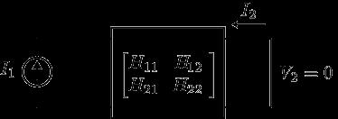
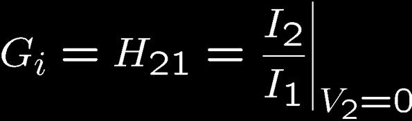
10 Device Current Gain H-parameters: Current gain: UC Berkeley EECS Copyright Prof. Ali M Niknejad
11 BJT Cross Section Most transistor action occurs in the small npn sandwich under the emitter. The base width should be made as small as possible in order to minimize recombination. The emitter doping should be much larger than the base doping to maximize electron injection into the base. A SiGe HBT transistor behaves very similarly to a normal BJT, but has lower base resistance rb since the doping in the base can be increased without compromising performance of the structure. UC Berkeley EECS Copyright Prof. Ali M Niknejad

12 Bipolar Small-Signal Model The resistor R π, dominates the input impedance at low frequency. At high frequency, though, C π dominates. C π is due to the collector-base reverse biased diode capacitance. C cs is the collector to substrate parasitic capacitance. In some processes, this is reduced with an oxide layer. C π has two components, due to the junction capacitance (forward-biased) and a diffusion capacitance UC Berkeley EECS Copyright Prof. Ali M Niknejad
, the bipolar has a much larger transconductance for the same current.")
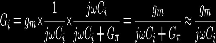
13 Bipolar Exponential Due to Boltzmann statistics, the collector current is described very accurately with an exponential relationship The device transconductance is therefore proportional to current where kt/q = 26mV at room temperature. Compare this to the equation for the FET. Since we usually have kt/q < (V gs -V T ), the bipolar has a much larger transconductance for the same current. This is the biggest advantage of a bipolar over a FET. UC Berkeley EECS Copyright Prof. Ali M Niknejad

14 Control Terminal Sensitivity 10 I C BJT: I C MOSFET: UC Berkeley EECS Copyright Prof. Ali M Niknejad


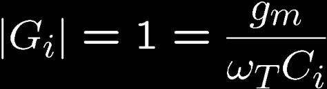
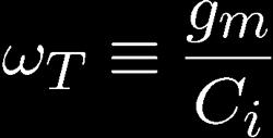
15 Bipolar Unity Gain Frequency The unity gain frequency of the BJT device is given by where we assumed the forward bias junction has C je ~ 2 C je0 Since the base-collector junction capacitance C π is a function of reverse bias, we should bias the collector voltage as high as possible for best performance. The diffusion capacitance is a function of collector current UC Berkeley EECS Copyright Prof. Ali M Niknejad

 UC Berkeley EECS 242 16 Copyright Prof.")
16 Bipolar Optimum Bias Point We can clearly see that if we continue to increase I C, then g m / I C increases and the limiting value of f T is given by the forward transit time In practice, though, we find that there is an optimum collector current. Beyond this current the transit time increases. This optimum point occurs due to the Kirk Effect. It s related to the base widening due to high level injection. (Not Star Trek!) UC Berkeley EECS Copyright Prof. Ali M Niknejad
17 BJT Base Transit Time E B C p n+ n+ Base transit time Current gain unity freq. R B W B n n+ buried layer p- substrate UC Berkeley EECS Copyright Prof. Ali M Niknejad
18 CMOS Cross Section Modern CMOS process has very short channel lengths (L < 100 nm). To ensure gate control of channel, as opposed to drain control (DIBL), we employ thin junctions and thin oxide (tox < 5 nm). Due to lithographic limitations, there is an overlap between the gate and the source/drain junctions. This leads to overlap capacitance. In a modern FET this is a substantial fraction of the gate capacitance (up to half). UC Berkeley EECS Copyright Prof. Ali M Niknejad

 region, the input capacitance is given by C gs R o is due to channel length modulation and other short channel effects")
19 FET Small Signal Model The junctions of a FET form reverse-biased pn junctions with the substrate (well), or the body node. This is another form of parasitic capacitance in the structure, C db and C sb. At DC, input is an open circuit. The input impedance has a small real part due to the gate resistance R g (polysilicon gate and NQS) and R s,d account for junction and contact resistance. In the forward active (saturation) region, the input capacitance is given by C gs R o is due to channel length modulation and other short channel effects (such as DIBL). UC Berkeley EECS Copyright Prof. Ali M Niknejad


20 FET Simplified Models For low frequencies, the resistors are ignored. But these resistors play an important role at high frequencies. If the source is tied to the bulk, then the model simplifies a lot more. Don t forget that layout parasitics increase the capacitance in the model, sometimes substantially (esp in deep submicron technologies). UC Berkeley EECS Copyright Prof. Ali M Niknejad
21 FET Unity Gain Frequency Long channel FET: Note that there is a peak f T since eventually the mobility of the transistor drops due to high vertical fields Short channel limit Bias dependent UC Berkeley EECS Copyright Prof. Ali M Niknejad

22 Scaling Speed Improvements CMOS transistors have steadily improved in performance just as predicted by theory. In the short channel regime the improvements are linear with scaling. At the same time, the decreasing supply voltage has led to a reduced dynamic range. Also the maximum gain has not improved as much UC Berkeley EECS Copyright Prof. Ali M Niknejad


23 Intrinsic Voltage Gain Important metric for analog circuits Communication circuits often work with low impedances in order to achieve high bandwidth, linearity, and matching. Inductive loads are also common to tune out the load capacitance and form a resonant circuit. The gain is thus given by To achieve high f T, the V dsat is relatively large so the current is increased to obtain sufficient gain. UC Berkeley EECS Copyright Prof. Ali M Niknejad
24 Normalized Gain For a bipolar device, the exponential current relationship results in a high constant normalized gain For a square law MOSFET, in saturation we have In weak inversion, the MOSFET is also exponential The factor n is set by the ratio of oxide to depletion capacitance UC Berkeley EECS Copyright Prof. Ali M Niknejad
25 MOSFET in subthreshold In sub-threshold, the surface potential varies linearity with V G The surface charge, and hence current, is thus exponentially related to V G V G V G C ox C dep Channel S _ D Bulk UC Berkeley EECS Copyright Prof. Ali M Niknejad
26 MOS Transconductor Efficiency Since the power dissipation is determined by and large by the DC current, we d like to get the most bang for the buck. From this perspective, the weak and moderate inversion region is the optimal place to operate. The price we pay is the speed of the device which decreases with decreasing V GS. Current drive is also very small. UC Berkeley EECS Copyright Prof. Ali M Niknejad
27 I-V Curves of Interest Typical I-V curves used to evaluate a technology/model: Drain Current v.s Vgs (Lg = 90nm) Drain Current v.s. Vds (Lg = 90 nm) Transconductance (Lg = 90nm) UC Berkeley EECS Copyright Prof. Ali M Niknejad
28 I-V Derivatives of Interest Most analog/rf circuits depend on the derivatives of the I- V relations (gm and ro) Output Conductance (Lg = 90 nm) Gm / Id (Lg = 1 µm) Output Conductance (Lg = 1 µm) UC Berkeley EECS Copyright Prof. Ali M Niknejad
29 High BJT Transconductance for fixed current, BJT gives more gain Precision Important in multiplication, log, and exponential functions More difficult in FETs due to process/temp. dependence I S process dependent in BJT use circuit tricks UC Berkeley EECS Copyright Prof. Ali M Niknejad
30 Advantages of BJT For high-speed applications, Need to bias in strong inversion Results in ~10x lower efficiency For a BJT, this relationship is fundamental and related to the Boltzman statistics (approximation of Fermi-Dirac statistics) For a MOSFET, this relationship is actually only valid for a square-law device and varies with V T (body bias) and temperature UC Berkeley EECS Copyright Prof. Ali M Niknejad
31 Maximum Two-Port Power Gain Y in Y out Y S Amp Y-Port Y L Condition: measure at maximum gain G max UC Berkeley EECS Copyright Prof. Ali M Niknejad


32 Maximum Power Gain Fmax f max = max. freq. of activity = freq. when {power gain = 1} UC Berkeley EECS Copyright Prof. Ali M Niknejad

33 FET Fmax Minimize all resistances R g use many small parallel gate fingers, <1 µm each R sb, R db, R bb substrate contacts <1 2 µm from device R s, R d don t use source/drain extensions to reduce L UC Berkeley EECS Copyright Prof. Ali M Niknejad

34 Advantage of BJT over FET (2) Better precision About 4 decades (420mV) of linearity Example: 420 mv Can build exp, log, roots, vector mag Lower 1/f noise corner Lower offset voltage UC Berkeley EECS Copyright Prof. Ali M Niknejad
35 Disadvantage of BJT r b hurts gain (power), NF SiGe allows fast transistors with low r b Exponential transfer function (advantage and disadvantage) Exponential non-linear restoration Expensive Lower volume than CMOS Absence of a switch Old CMOS gets cheaper! 0.065um ~ $1M (mask) 0.13um ~ $40k UC Berkeley EECS Copyright Prof. Ali M Niknejad
36 Advantage of FET over BJT Cheaper and more widely available (many fabs in US, Asia, and Europe) Square law less distortion P-FET widely available Triode region variable resistor Widely available digital logic Low leakage in gates Sample and hold (S/H) and switch cap filters (SCF) Dense digital circuitry / DSP for calibration Offset voltages and mismatches can be compensated digitally Dense metal layers allows MIM ( MOM ) capacitors for free UC Berkeley EECS Copyright Prof. Ali M Niknejad
37 Higher Performance: SiGe Technology e Depletion region due to reverse bias n + p n Problem: As W B decreases r b increases Solution: SiGe base allows for higher f T without reducing W B h + E B C E B C W B p n+ n+ R B W B n n+ buried layer p- substrate UC Berkeley EECS Copyright Prof. Ali M Niknejad
38 SiGe HBT Action A SiGe BJT is often called a HBT (heterojunction bipolar transistor) Ge epitaxially grown in base Causes strain in crystal Causes extra potential barrier for holes (majority carrier) in the base from flowing into emitter Beneficial effects W B decreases N B increases r b low N E decreases C j decreases UC Berkeley EECS Copyright Prof. Ali M Niknejad
39 GaAs/InP Technology One of the primary advantages of the III-V based transistors is the higher peak mobility compared to Si. The insulating substrate also allows higher Q passives. The extra cost of these technologies limits it to niche applications such as very high frequencies, high performance, and power amplifiers. UC Berkeley EECS Copyright Prof. Ali M Niknejad
40 FinFETs and Multigate Transistors To combat the problems with scaling of MOSFETs below 45nm, Berkeley researchers introduced the FinFET, a double gate device. Due to thin body and double gates, there is better gate control as opposed to drain control, leading to enhanced output resistance and lower leakage in subthreshold. UC Berkeley EECS Copyright Prof. Ali M Niknejad
41 FinFET Structure and Layout Gate straddles thin silicon fin, forming two conducting channels on sidewall Bulk-Si MOSFET Source (all images): T-J King, et al, FinFET Technology Optimization presentation slides, Oct Multi-fin layout UC Berkeley EECS Copyright Prof. Ali M Niknejad
42 An Aside on Thermal Conductivity GaAs Si Semi-insulating substrate Not very good conductor of heat High quality passive elements (next topic) Semi-conducting substrate Good conductor of heat Lossy substrate leads to lower quality passives UC Berkeley EECS Copyright Prof. Ali M Niknejad

43 An Aside on Thermal conductivity (2) Also depends on packaging Example: in flip-chip bonding, thermal conductivity function of # of bumps rather than substrate Back-side of die can lose heat through radiation or convection through air but thermal contact is much more effective Package heat Die heat Flip chip bonding Wire bonding UC Berkeley EECS Copyright Prof. Ali M Niknejad
44 References and Further Reading UCB EECS 142/242 Class Notes (Niknejad/Meyer) UCB EECS 240 Class Notes, (Niknejad/Boser) Analysis and design of analog integrated circuits, Paul R. Gray, Robert G. Meyer. 3rd ed. New York : Wiley, c1993. Microwave CMOS-device physics and design, Manku, T., IEEE Journal of Solid-State Circuits, vol.34, (no.3), March p UC Berkeley EECS Copyright Prof. Ali M Niknejad
EE70 - Intro. Electronics
 EE70 - Intro. Electronics Course website: ~/classes/ee70/fall05 Today s class agenda (November 28, 2005) review Serial/parallel resonant circuits Diode Field Effect Transistor (FET) f 0 = Qs = Qs = 1 2π
Field-Effect Transistor (FET) is one of the two major transistors; FET derives its name from its working mechanism;
 is one of the two major transistors; FET derives its name from its working mechanism;") Chapter 3 Field-Effect Transistors (FETs) 3.1 Introduction Field-Effect Transistor (FET) is one of the two major transistors; FET derives its name from its working mechanism; The concept has been known
Chapter 3 Field-Effect Transistors (FETs) 3.1 Introduction Field-Effect Transistor (FET) is one of the two major transistors; FET derives its name from its working mechanism; The concept has been known
Student Lecture by: Giangiacomo Groppi Joel Cassell Pierre Berthelot September 28 th 2004
 Student Lecture by: Giangiacomo Groppi Joel Cassell Pierre Berthelot September 28 th 2004 Lecture outline Historical introduction Semiconductor devices overview Bipolar Junction Transistor (BJT) Field
UNIT 3: FIELD EFFECT TRANSISTORS
 FIELD EFFECT TRANSISTOR: UNIT 3: FIELD EFFECT TRANSISTORS The field effect transistor is a semiconductor device, which depends for its operation on the control of current by an electric field. There are
Three Terminal Devices
 Three Terminal Devices - field effect transistor (FET) - bipolar junction transistor (BJT) - foundation on which modern electronics is built - active devices - devices described completely by considering
UNIT 3 Transistors JFET
 UNIT 3 Transistors JFET Mosfet Definition of BJT A bipolar junction transistor is a three terminal semiconductor device consisting of two p-n junctions which is able to amplify or magnify a signal. It
UNIVERSITY OF CALIFORNIA AT BERKELEY College of Engineering Department of Electrical Engineering and Computer Sciences.
 UNIVERSITY OF CALIFORNIA AT BERKELEY College of Engineering Department of Electrical Engineering and Computer Sciences Discussion #9 EE 05 Spring 2008 Prof. u MOSFETs The standard MOSFET structure is shown
ANALYSIS AND DESIGN OF ANALOG INTEGRATED CIRCUITS
 ANALYSIS AND DESIGN OF ANALOG INTEGRATED CIRCUITS Fourth Edition PAUL R. GRAY University of California, Berkeley PAUL J. HURST University of California, Davis STEPHEN H. LEWIS University of California,
EECS130 Integrated Circuit Devices
 EECS130 Integrated Circuit Devices Professor Ali Javey 11/6/2007 MOSFETs Lecture 6 BJTs- Lecture 1 Reading Assignment: Chapter 10 More Scalable Device Structures Vertical Scaling is important. For example,
EE301 Electronics I , Fall
 EE301 Electronics I 2018-2019, Fall 1. Introduction to Microelectronics (1 Week/3 Hrs.) Introduction, Historical Background, Basic Consepts 2. Rewiev of Semiconductors (1 Week/3 Hrs.) Semiconductor materials
Field Effect Transistors
 Field Effect Transistors LECTURE NO. - 41 Field Effect Transistors www.mycsvtunotes.in JFET MOSFET CMOS Field Effect transistors - FETs First, why are we using still another transistor? BJTs had a small
Semiconductor Physics and Devices
 Metal-Semiconductor and Semiconductor Heterojunctions The Metal-Oxide-Semiconductor Field-Effect Transistor (MOSFET) is one of two major types of transistors. The MOSFET is used in digital circuit, because
NAME: Last First Signature
 UNIVERSITY OF CALIFORNIA, BERKELEY College of Engineering Department of Electrical Engineering and Computer Sciences EE 130: IC Devices Spring 2003 FINAL EXAMINATION NAME: Last First Signature STUDENT
Digital Electronics. By: FARHAD FARADJI, Ph.D. Assistant Professor, Electrical and Computer Engineering, K. N. Toosi University of Technology
 K. N. Toosi University of Technology Chapter 7. Field-Effect Transistors By: FARHAD FARADJI, Ph.D. Assistant Professor, Electrical and Computer Engineering, K. N. Toosi University of Technology http://wp.kntu.ac.ir/faradji/digitalelectronics.htm
UNIT-1 Bipolar Junction Transistors. Text Book:, Microelectronic Circuits 6 ed., by Sedra and Smith, Oxford Press
 UNIT-1 Bipolar Junction Transistors Text Book:, Microelectronic Circuits 6 ed., by Sedra and Smith, Oxford Press Figure 6.1 A simplified structure of the npn transistor. Microelectronic Circuits, Sixth
ANALYSIS AND DESIGN OF ANALOG INTEGRATED CIRCUITS
 ANALYSIS AND DESIGN OF ANALOG INTEGRATED CIRCUITS Fourth Edition PAUL R. GRAY University of California, Berkeley PAUL J. HURST University of California, Davis STEPHEN H. LEWIS University of California,
Conduction Characteristics of MOS Transistors (for fixed Vds)! Topic 2. Basic MOS theory & SPICE simulation. MOS Transistor
! Topic 2. Basic MOS theory & SPICE simulation. MOS Transistor") Conduction Characteristics of MOS Transistors (for fixed Vds)! Topic 2 Basic MOS theory & SPICE simulation Peter Cheung Department of Electrical & Electronic Engineering Imperial College London (Weste&Harris,
Conduction Characteristics of MOS Transistors (for fixed Vds)! Topic 2 Basic MOS theory & SPICE simulation Peter Cheung Department of Electrical & Electronic Engineering Imperial College London (Weste&Harris,
Topic 2. Basic MOS theory & SPICE simulation
 Topic 2 Basic MOS theory & SPICE simulation Peter Cheung Department of Electrical & Electronic Engineering Imperial College London (Weste&Harris, Ch 2 & 5.1-5.3 Rabaey, Ch 3) URL: www.ee.ic.ac.uk/pcheung/
Conduction Characteristics of MOS Transistors (for fixed Vds) Topic 2. Basic MOS theory & SPICE simulation. MOS Transistor
 Topic 2. Basic MOS theory & SPICE simulation. MOS Transistor") Conduction Characteristics of MOS Transistors (for fixed Vds) Topic 2 Basic MOS theory & SPICE simulation Peter Cheung Department of Electrical & Electronic Engineering Imperial College London (Weste&Harris,
Conduction Characteristics of MOS Transistors (for fixed Vds) Topic 2 Basic MOS theory & SPICE simulation Peter Cheung Department of Electrical & Electronic Engineering Imperial College London (Weste&Harris,
MOS Field-Effect Transistors (MOSFETs)
") 6 MOS Field-Effect Transistors (MOSFETs) A three-terminal device that uses the voltages of the two terminals to control the current flowing in the third terminal. The basis for amplifier design. The basis
6 MOS Field-Effect Transistors (MOSFETs) A three-terminal device that uses the voltages of the two terminals to control the current flowing in the third terminal. The basis for amplifier design. The basis
MOS Capacitance and Introduction to MOSFETs
 ECE-305: Fall 2016 MOS Capacitance and Introduction to MOSFETs Professor Peter Bermel Electrical and Computer Engineering Purdue University, West Lafayette, IN USA pbermel@purdue.edu 11/4/2016 Pierret,
Field Effect Transistors (npn)
") Field Effect Transistors (npn) gate drain source FET 3 terminal device channel e - current from source to drain controlled by the electric field generated by the gate base collector emitter BJT 3 terminal
Field Effect Transistors (npn) gate drain source FET 3 terminal device channel e - current from source to drain controlled by the electric field generated by the gate base collector emitter BJT 3 terminal
Chapter 8. Field Effect Transistor
 Chapter 8. Field Effect Transistor Field Effect Transistor: The field effect transistor is a semiconductor device, which depends for its operation on the control of current by an electric field. There
Sub-Threshold Region Behavior of Long Channel MOSFET
 Sub-threshold Region - So far, we have discussed the MOSFET behavior in linear region and saturation region - Sub-threshold region is refer to region where Vt is less than Vt - Sub-threshold region reflects
EE 42/100 Lecture 23: CMOS Transistors and Logic Gates. Rev A 4/15/2012 (10:39 AM) Prof. Ali M. Niknejad
 Prof. Ali M. Niknejad") A. M. Niknejad University of California, Berkeley EE 100 / 42 Lecture 23 p. 1/16 EE 42/100 Lecture 23: CMOS Transistors and Logic Gates ELECTRONICS Rev A 4/15/2012 (10:39 AM) Prof. Ali M. Niknejad University
A. M. Niknejad University of California, Berkeley EE 100 / 42 Lecture 23 p. 1/16 EE 42/100 Lecture 23: CMOS Transistors and Logic Gates ELECTRONICS Rev A 4/15/2012 (10:39 AM) Prof. Ali M. Niknejad University
Questions on JFET: 1) Which of the following component is a unipolar device?
 Which of the following component is a unipolar device?") Questions on JFET: 1) Which of the following component is a unipolar device? a) BJT b) FET c) DJT d) EFT 2) Current Conduction in FET takes place due e) Majority charge carriers only f) Minority charge
Questions on JFET: 1) Which of the following component is a unipolar device? a) BJT b) FET c) DJT d) EFT 2) Current Conduction in FET takes place due e) Majority charge carriers only f) Minority charge
Lecture-45. MOS Field-Effect-Transistors Threshold voltage
 Lecture-45 MOS Field-Effect-Transistors 7.4. Threshold voltage In this section we summarize the calculation of the threshold voltage and discuss the dependence of the threshold voltage on the bias applied
Lecture 020 ECE4430 Review II (1/5/04) Page 020-1
 Page 020-1") Lecture 020 ECE4430 Review II (1/5/04) Page 020-1 LECTURE 020 ECE 4430 REVIEW II (READING: GHLM - Chap. 2) Objective The objective of this presentation is: 1.) Identify the prerequisite material as taught
Lecture 020 ECE4430 Review II (1/5/04) Page 020-1 LECTURE 020 ECE 4430 REVIEW II (READING: GHLM - Chap. 2) Objective The objective of this presentation is: 1.) Identify the prerequisite material as taught
Unit III FET and its Applications. 2 Marks Questions and Answers
 Unit III FET and its Applications 2 Marks Questions and Answers 1. Why do you call FET as field effect transistor? The name field effect is derived from the fact that the current is controlled by an electric
Index. Small-Signal Models, 14 saturation current, 3, 5 Transistor Cutoff Frequency, 18 transconductance, 16, 22 transit time, 10
 Index A absolute value, 308 additional pole, 271 analog multiplier, 190 B BiCMOS,107 Bode plot, 266 base-emitter voltage, 16, 50 base-emitter voltages, 296 bias current, 111, 124, 133, 137, 166, 185 bipolar
Basic Electronics. Introductory Lecture Course for. Technology and Instrumentation in Particle Physics Chicago, Illinois June 9-14, 2011
 Basic Electronics Introductory Lecture Course for Technology and Instrumentation in Particle Physics 2011 Chicago, Illinois June 9-14, 2011 Presented By Gary Drake Argonne National Laboratory Session 3
Department of Electrical Engineering IIT Madras
 Department of Electrical Engineering IIT Madras Sample Questions on Semiconductor Devices EE3 applicants who are interested to pursue their research in microelectronics devices area (fabrication and/or
Lecture 3: Transistors
 Lecture 3: Transistors Now that we know about diodes, let s put two of them together, as follows: collector base emitter n p n moderately doped lightly doped, and very thin heavily doped At first glance,
MOSFET Parasitic Elements
 MOSFET Parasitic Elements Three MITs of the ay Components of the source resistance and their influence on g m and R d Gate-induced drain leakage (GIL) and its effect on lowest possible leakage current
MOSFET & IC Basics - GATE Problems (Part - I)
") MOSFET & IC Basics - GATE Problems (Part - I) 1. Channel current is reduced on application of a more positive voltage to the GATE of the depletion mode n channel MOSFET. (True/False) [GATE 1994: 1 Mark]
MOSFET & IC Basics - GATE Problems (Part - I) 1. Channel current is reduced on application of a more positive voltage to the GATE of the depletion mode n channel MOSFET. (True/False) [GATE 1994: 1 Mark]
Chapter 4. CMOS Cascode Amplifiers. 4.1 Introduction. 4.2 CMOS Cascode Amplifiers
 Chapter 4 CMOS Cascode Amplifiers 4.1 Introduction A single stage CMOS amplifier cannot give desired dc voltage gain, output resistance and transconductance. The voltage gain can be made to attain higher
value of W max for the device. The at band voltage is -0.9 V. Problem 5: An Al-gate n-channel MOS capacitor has a doping of N a = cm ;3. The oxi
 Prof. Jasprit Singh Fall 2001 EECS 320 Homework 10 This homework is due on December 6 Problem 1: An n-type In 0:53 Ga 0:47 As epitaxial layer doped at 10 16 cm ;3 is to be used as a channel in a FET. A
I E I C since I B is very small
 Figure 2: Symbols and nomenclature of a (a) npn and (b) pnp transistor. The BJT consists of three regions, emitter, base, and collector. The emitter and collector are usually of one type of doping, while
Semiconductor Devices
 Semiconductor Devices Modelling and Technology Source Electrons Gate Holes Drain Insulator Nandita DasGupta Amitava DasGupta SEMICONDUCTOR DEVICES Modelling and Technology NANDITA DASGUPTA Professor Department
Solid State Devices- Part- II. Module- IV
 Solid State Devices- Part- II Module- IV MOS Capacitor Two terminal MOS device MOS = Metal- Oxide- Semiconductor MOS capacitor - the heart of the MOSFET The MOS capacitor is used to induce charge at the
EIE209 Basic Electronics. Transistor Devices. Contents BJT and FET Characteristics Operations. Prof. C.K. Tse: T ransistor devices
 EIE209 Basic Electronics Transistor Devices Contents BJT and FET Characteristics Operations 1 What is a transistor? Three-terminal device whose voltage-current relationship is controlled by a third voltage
55:041 Electronic Circuits
 55:041 Electronic Circuits MOSFETs Sections of Chapter 3 &4 A. Kruger MOSFETs, Page-1 Basic Structure of MOS Capacitor Sect. 3.1 Width = 1 10-6 m or less Thickness = 50 10-9 m or less ` MOS Metal-Oxide-Semiconductor
INTRODUCTION: Basic operating principle of a MOSFET:
 INTRODUCTION: Along with the Junction Field Effect Transistor (JFET), there is another type of Field Effect Transistor available whose Gate input is electrically insulated from the main current carrying
Lecture 16: MOS Transistor models: Linear models, SPICE models. Context. In the last lecture, we discussed the MOS transistor, and
 Lecture 16: MOS Transistor models: Linear models, SPICE models Context In the last lecture, we discussed the MOS transistor, and added a correction due to the changing depletion region, called the body
Difference between BJTs and FETs. Junction Field Effect Transistors (JFET)
") Difference between BJTs and FETs Transistors can be categorized according to their structure, and two of the more commonly known transistor structures, are the BJT and FET. The comparison between BJTs
Difference between BJTs and FETs Transistors can be categorized according to their structure, and two of the more commonly known transistor structures, are the BJT and FET. The comparison between BJTs
MOSFET short channel effects
 MOSFET short channel effects overview Five different short channel effects can be distinguished: velocity saturation drain induced barrier lowering (DIBL) impact ionization surface scattering hot electrons
Analog and Telecommunication Electronics
 Politecnico di Torino - ICT School Analog and Telecommunication Electronics F2 Active power devices»mos»bjt» IGBT, TRIAC» Safe Operating Area» Thermal analysis 30/05/2012-1 ATLCE - F2-2011 DDC Lesson F2:
PHYS 3050 Electronics I
 PHYS 3050 Electronics I Chapter 4. Semiconductor Diodes and Transistors Earth, Moon, Mars, and Beyond Dr. Jinjun Shan, Associate Professor of Space Engineering Department of Earth and Space Science and
PHYSICS OF SEMICONDUCTOR DEVICES
 PHYSICS OF SEMICONDUCTOR DEVICES PHYSICS OF SEMICONDUCTOR DEVICES by J. P. Colinge Department of Electrical and Computer Engineering University of California, Davis C. A. Colinge Department of Electrical
Power MOSFET Zheng Yang (ERF 3017,
 ECE442 Power Semiconductor Devices and Integrated Circuits Power MOSFET Zheng Yang (ERF 3017, email: yangzhen@uic.edu) Evolution of low-voltage (
Chapter 5: Field Effect Transistors
 Chapter 5: Field Effect Transistors Slide 1 FET FET s (Field Effect Transistors) are much like BJT s (Bipolar Junction Transistors). Similarities: Amplifiers Switching devices Impedance matching circuits
FIELD EFFECT TRANSISTOR (FET) 1. JUNCTION FIELD EFFECT TRANSISTOR (JFET)
 1. JUNCTION FIELD EFFECT TRANSISTOR (JFET)") FIELD EFFECT TRANSISTOR (FET) The field-effect transistor (FET) is a three-terminal device used for a variety of applications that match, to a large extent, those of the BJT transistor. Although there
FIELD EFFECT TRANSISTOR (FET) The field-effect transistor (FET) is a three-terminal device used for a variety of applications that match, to a large extent, those of the BJT transistor. Although there
Basic Fabrication Steps
 Basic Fabrication Steps and Layout Somayyeh Koohi Department of Computer Engineering Adapted with modifications from lecture notes prepared by author Outline Fabrication steps Transistor structures Transistor
UNIT-VI FIELD EFFECT TRANSISTOR. 1. Explain about the Field Effect Transistor and also mention types of FET s.
 UNIT-I FIELD EFFECT TRANSISTOR 1. Explain about the Field Effect Transistor and also mention types of FET s. The Field Effect Transistor, or simply FET however, uses the voltage that is applied to their
444 Index. F Fermi potential, 146 FGMOS transistor, 20 23, 57, 83, 84, 98, 205, 208, 213, 215, 216, 241, 242, 251, 280, 311, 318, 332, 354, 407
 Index A Accuracy active resistor structures, 46, 323, 328, 329, 341, 344, 360 computational circuits, 171 differential amplifiers, 30, 31 exponential circuits, 285, 291, 292 multifunctional structures,
6. Field-Effect Transistor
 6. Outline: Introduction to three types of FET: JFET MOSFET & CMOS MESFET Constructions, Characteristics & Transfer curves of: JFET & MOSFET Introduction The field-effect transistor (FET) is a threeterminal
MEASUREMENT AND INSTRUMENTATION STUDY NOTES UNIT-I
 MEASUREMENT AND INSTRUMENTATION STUDY NOTES The MOSFET The MOSFET Metal Oxide FET UNIT-I As well as the Junction Field Effect Transistor (JFET), there is another type of Field Effect Transistor available
MTLE-6120: Advanced Electronic Properties of Materials. Semiconductor transistors for logic and memory. Reading: Kasap
 MTLE-6120: Advanced Electronic Properties of Materials 1 Semiconductor transistors for logic and memory Reading: Kasap 6.6-6.8 Vacuum tube diodes 2 Thermionic emission from cathode Electrons collected
FUNDAMENTALS OF MODERN VLSI DEVICES
 19-13- FUNDAMENTALS OF MODERN VLSI DEVICES YUAN TAUR TAK H. MING CAMBRIDGE UNIVERSITY PRESS Physical Constants and Unit Conversions List of Symbols Preface page xi xiii xxi 1 INTRODUCTION I 1.1 Evolution
Review Energy Bands Carrier Density & Mobility Carrier Transport Generation and Recombination
 Review Energy Bands Carrier Density & Mobility Carrier Transport Generation and Recombination Current Transport: Diffusion, Thermionic Emission & Tunneling For Diffusion current, the depletion layer is
CONTENTS. 2.2 Schrodinger's Wave Equation 31. PART I Semiconductor Material Properties. 2.3 Applications of Schrodinger's Wave Equation 34
 CONTENTS Preface x Prologue Semiconductors and the Integrated Circuit xvii PART I Semiconductor Material Properties CHAPTER 1 The Crystal Structure of Solids 1 1.0 Preview 1 1.1 Semiconductor Materials
Alternatives to standard MOSFETs. What problems are we really trying to solve?
 Alternatives to standard MOSFETs A number of alternative FET schemes have been proposed, with an eye toward scaling up to the 10 nm node. Modifications to the standard MOSFET include: Silicon-in-insulator
INTRODUCTION TO MOS TECHNOLOGY
 INTRODUCTION TO MOS TECHNOLOGY 1. The MOS transistor The most basic element in the design of a large scale integrated circuit is the transistor. For the processes we will discuss, the type of transistor
An introduction to Depletion-mode MOSFETs By Linden Harrison
 An introduction to Depletion-mode MOSFETs By Linden Harrison Since the mid-nineteen seventies the enhancement-mode MOSFET has been the subject of almost continuous global research, development, and refinement
Lecture - 18 Transistors
 Electronic Materials, Devices and Fabrication Dr. S. Prarasuraman Department of Metallurgical and Materials Engineering Indian Institute of Technology, Madras Lecture - 18 Transistors Last couple of classes
Reg. No. : Question Paper Code : B.E./B.Tech. DEGREE EXAMINATION, NOVEMBER/DECEMBER Second Semester
 WK 5 Reg. No. : Question Paper Code : 27184 B.E./B.Tech. DEGREE EXAMINATION, NOVEMBER/DECEMBER 2015. Time : Three hours Second Semester Electronics and Communication Engineering EC 6201 ELECTRONIC DEVICES
Semiconductor Devices
 Semiconductor Devices - 2014 Lecture Course Part of SS Module PY4P03 Dr. P. Stamenov School of Physics and CRANN, Trinity College, Dublin 2, Ireland Hilary Term, TCD 3 th of Feb 14 MOSFET Unmodified Channel
INTERNATIONAL JOURNAL OF APPLIED ENGINEERING RESEARCH, DINDIGUL Volume 1, No 3, 2010
 Low Power CMOS Inverter design at different Technologies Vijay Kumar Sharma 1, Surender Soni 2 1 Department of Electronics & Communication, College of Engineering, Teerthanker Mahaveer University, Moradabad
Solid State Device Fundamentals
 Solid State Device Fundamentals 4.4. Field Effect Transistor (MOSFET) ENS 463 Lecture Course by Alexander M. Zaitsev alexander.zaitsev@csi.cuny.edu Tel: 718 982 2812 4N101b 1 Field-effect transistor (FET)
COMPARISON OF THE MOSFET AND THE BJT:
 COMPARISON OF THE MOSFET AND THE BJT: In this section we present a comparison of the characteristics of the two major electronic devices: the MOSFET and the BJT. To facilitate this comparison, typical
COLLECTOR DRAIN BASE GATE EMITTER. Applying a voltage to the Gate connection allows current to flow between the Drain and Source connections.
 MOSFETS Although the base current in a transistor is usually small (< 0.1 ma), some input devices (e.g. a crystal microphone) may be limited in their output. In order to overcome this, a Field Effect Transistor
Section 2.3 Bipolar junction transistors - BJTs
 Section 2.3 Bipolar junction transistors - BJTs Single junction devices, such as p-n and Schottkty diodes can be used to obtain rectifying I-V characteristics, and to form electronic switching circuits
Chapter 1. Introduction
 EECS3611 Analog Integrated Circuit esign Chapter 1 Introduction EECS3611 Analog Integrated Circuit esign Instructor: Prof. Ebrahim Ghafar-Zadeh, Prof. Peter Lian email: egz@cse.yorku.ca peterlian@cse.yorku.ca
Session 10: Solid State Physics MOSFET
 Session 10: Solid State Physics MOSFET 1 Outline A B C D E F G H I J 2 MOSCap MOSFET Metal-Oxide-Semiconductor Field-Effect Transistor: Al (metal) SiO2 (oxide) High k ~0.1 ~5 A SiO2 A n+ n+ p-type Si (bulk)
Davinci. Semiconductor Device Simulaion in 3D SYSTEMS PRODUCTS LOGICAL PRODUCTS PHYSICAL IMPLEMENTATION SIMULATION AND ANALYSIS LIBRARIES TCAD
 SYSTEMS PRODUCTS LOGICAL PRODUCTS PHYSICAL IMPLEMENTATION SIMULATION AND ANALYSIS LIBRARIES TCAD Aurora DFM WorkBench Davinci Medici Raphael Raphael-NES Silicon Early Access TSUPREM-4 Taurus-Device Taurus-Lithography
Depletion-mode operation ( 공핍형 ): Using an input gate voltage to effectively decrease the channel size of an FET
: Using an input gate voltage to effectively decrease the channel size of an FET") Ch. 13 MOSFET Metal-Oxide-Semiconductor Field-Effect Transistor : I D D-mode E-mode V g The gate oxide is made of dielectric SiO 2 with e = 3.9 Depletion-mode operation ( 공핍형 ): Using an input gate voltage
Ch. 13 MOSFET Metal-Oxide-Semiconductor Field-Effect Transistor : I D D-mode E-mode V g The gate oxide is made of dielectric SiO 2 with e = 3.9 Depletion-mode operation ( 공핍형 ): Using an input gate voltage
Session 2 MOS Transistor for RF Circuits
 Session 2 MOS Transistor for RF Circuits Session Speaker Chandramohan P. Session Contents MOS transistor basics MOS equivalent circuit Single stage amplifiers Opamp design Session objectives To understand
ECE520 VLSI Design. Lecture 2: Basic MOS Physics. Payman Zarkesh-Ha
 ECE520 VLSI Design Lecture 2: Basic MOS Physics Payman Zarkesh-Ha Office: ECE Bldg. 230B Office hours: Wednesday 2:00-3:00PM or by appointment E-mail: pzarkesh@unm.edu Slide: 1 Review of Last Lecture Semiconductor
Week 7: Common-Collector Amplifier, MOS Field Effect Transistor
 EE 2110A Electronic Circuits Week 7: Common-Collector Amplifier, MOS Field Effect Transistor ecture 07-1 Topics to coer Common-Collector Amplifier MOS Field Effect Transistor Physical Operation and I-V
Power Semiconductor Devices
 TRADEMARK OF INNOVATION Power Semiconductor Devices Introduction This technical article is dedicated to the review of the following power electronics devices which act as solid-state switches in the circuits.
FET(Field Effect Transistor)
") Field Effect Transistor: Construction and Characteristic of JFETs. Transfer Characteristic. CS,CD,CG amplifier and analysis of CS amplifier MOSFET (Depletion and Enhancement) Type, Transfer Characteristic,
Field Effect Transistor: Construction and Characteristic of JFETs. Transfer Characteristic. CS,CD,CG amplifier and analysis of CS amplifier MOSFET (Depletion and Enhancement) Type, Transfer Characteristic,
EE 5611 Introduction to Microelectronic Technologies Fall Thursday, September 04, 2014 Lecture 02
 EE 5611 Introduction to Microelectronic Technologies Fall 2014 Thursday, September 04, 2014 Lecture 02 1 Lecture Outline Review on semiconductor materials Review on microelectronic devices Example of microelectronic
Basic Electronics Prof. Dr. Chitralekha Mahanta Department of Electronics and Communication Engineering Indian Institute of Technology, Guwahati
 Basic Electronics Prof. Dr. Chitralekha Mahanta Department of Electronics and Communication Engineering Indian Institute of Technology, Guwahati Module: 3 Field Effect Transistors Lecture-7 High Frequency
Field Effect Transistors
 Chapter 5: Field Effect Transistors Slide 1 FET FET s (Field Effect Transistors) are much like BJT s (Bipolar Junction Transistors). Similarities: Amplifiers Switching devices Impedance matching circuits
6.776 High Speed Communication Circuits Lecture 6 MOS Transistors, Passive Components, Gain- Bandwidth Issue for Broadband Amplifiers
 6.776 High Speed Communication Circuits Lecture 6 MOS Transistors, Passive Components, Gain- Bandwidth Issue for Broadband Amplifiers Massachusetts Institute of Technology February 17, 2005 Copyright 2005
FET. Field Effect Transistors ELEKTRONIKA KONTROL. Eka Maulana, ST, MT, M.Eng. Universitas Brawijaya. p + S n n-channel. Gate. Basic structure.
 FET Field Effect Transistors ELEKTRONIKA KONTROL Basic structure Gate G Source S n n-channel Cross section p + p + p + G Depletion region Drain D Eka Maulana, ST, MT, M.Eng. Universitas Brawijaya S Channel
SRM INSTITUTE OF SCIENCE AND TECHNOLOGY (DEEMED UNIVERSITY)
") SRM INSTITUTE OF SCIENCE AND TECHNOLOGY (DEEMED UNIVERSITY) QUESTION BANK I YEAR B.Tech (II Semester) ELECTRONIC DEVICES (COMMON FOR EC102, EE104, IC108, BM106) UNIT-I PART-A 1. What are intrinsic and
SRM INSTITUTE OF SCIENCE AND TECHNOLOGY (DEEMED UNIVERSITY) QUESTION BANK I YEAR B.Tech (II Semester) ELECTRONIC DEVICES (COMMON FOR EC102, EE104, IC108, BM106) UNIT-I PART-A 1. What are intrinsic and
55:041 Electronic Circuits
 55:041 Electronic Circuits Mosfet Review Sections of Chapter 3 &4 A. Kruger Mosfet Review, Page-1 Basic Structure of MOS Capacitor Sect. 3.1 Width 1 10-6 m or less Thickness 50 10-9 m or less ` MOS Metal-Oxide-Semiconductor
JFET 101, a Tutorial Look at the Junction Field Effect Transistor 8May 2007, edit 2April2016, Wes Hayward, w7zoi
 JFET 101, a Tutorial Look at the Junction Field Effect Transistor 8May 2007, edit 2April2016, Wes Hayward, w7zoi FETs are popular among experimenters, but they are not as universally understood as the
Prof. Paolo Colantonio a.a
 Prof. Paolo Colantonio a.a. 20 2 Field effect transistors (FETs) are probably the simplest form of transistor, widely used in both analogue and digital applications They are characterised by a very high
Physics of Bipolar Transistor
 Physics of Bipolar Transistor Motivations - In many electronic applications, amplifier is the most fundamental building block. Ex Audio amplifier: amplifies electric signal to drive a speaker RF Power
EC6202-ELECTRONIC DEVICES AND CIRCUITS YEAR/SEM: II/III UNIT 1 TWO MARKS. 1. Define diffusion current.
 EC6202-ELECTRONIC DEVICES AND CIRCUITS YEAR/SEM: II/III UNIT 1 TWO MARKS 1. Define diffusion current. A movement of charge carriers due to the concentration gradient in a semiconductor is called process
Lecture 190 CMOS Technology, Compatible Devices (10/28/01) Page 190-1
 Page 190-1") Lecture 190 CMOS Technology, Compatible Devices (10/28/01) Page 190-1 LECTURE 190 CMOS TECHNOLOGY-COMPATIBLE DEVICES (READING: Text-Sec. 2.9) INTRODUCTION Objective The objective of this presentation is
Lecture 190 CMOS Technology, Compatible Devices (10/28/01) Page 190-1 LECTURE 190 CMOS TECHNOLOGY-COMPATIBLE DEVICES (READING: Text-Sec. 2.9) INTRODUCTION Objective The objective of this presentation is
Device Technologies. Yau - 1
 Device Technologies Yau - 1 Objectives After studying the material in this chapter, you will be able to: 1. Identify differences between analog and digital devices and passive and active components. Explain
ES 330 Electronics II Homework # 1 (Fall 2016 SOLUTIONS)
") SOLUTIONS ES 330 Electronics II Homework # 1 (Fall 2016 SOLUTIONS) Problem 1 (20 points) We know that a pn junction diode has an exponential I-V behavior when forward biased. The diode equation relating
SOLUTIONS ES 330 Electronics II Homework # 1 (Fall 2016 SOLUTIONS) Problem 1 (20 points) We know that a pn junction diode has an exponential I-V behavior when forward biased. The diode equation relating
Design cycle for MEMS
 Design cycle for MEMS Design cycle for ICs IC Process Selection nmos CMOS BiCMOS ECL for logic for I/O and driver circuit for critical high speed parts of the system The Real Estate of a Wafer MOS Transistor
BJT Amplifier. Superposition principle (linear amplifier)
") BJT Amplifier Two types analysis DC analysis Applied DC voltage source AC analysis Time varying signal source Superposition principle (linear amplifier) The response of a linear amplifier circuit excited
BJT Amplifier Two types analysis DC analysis Applied DC voltage source AC analysis Time varying signal source Superposition principle (linear amplifier) The response of a linear amplifier circuit excited
Chapter 3: Basics Semiconductor Devices and Processing 2006/9/27 1. Topics
 Chapter 3: Basics Semiconductor Devices and Processing 2006/9/27 1 Topics What is semiconductor Basic semiconductor devices Basics of IC processing CMOS technologies 2006/9/27 2 1 What is Semiconductor
Lesson 5. Electronics: Semiconductors Doping p-n Junction Diode Half Wave and Full Wave Rectification Introduction to Transistors-
 Lesson 5 Electronics: Semiconductors Doping p-n Junction Diode Half Wave and Full Wave Rectification Introduction to Transistors- Types and Connections Semiconductors Semiconductors If there are many free