ASCENT Overview. European Nanoelectronics Infrastructure Access. MOS-AK Workshop, Infineon, Munich, 13 th March 2018.
|
|
|
- Jonah Fields
- 5 years ago
- Views:
Transcription


1 ASCENT Overview MOS-AK Workshop, Infineon, Munich, 13 th March 2018 European Nanoelectronics Infrastructure Access Paul Roseingrave


2 The Challenge Cost/performance returns by scaling are diminishing Cost to achieve tape out on new nodes is increasing Technology Quarterly March 12, 2016

3 The infrastructure Unique opportunity: ASCENT combines Tyndall, imec and CEA-Leti s nanofabrication & electrical characterisation capabilities into a single research infrastructure and makes it accessible to all
4 Objectives ASCENT will: Leverage Europe s Unique advantage in nanofabrication to strengthen modeling and characterisation research community Accelerate development of advanced models at scales of 14nm and below Provide characterisation community with access to advanced test chips, flexible fabrication and advanced test and characterisation equipment Make project outputs available and easily accessible to nanoelectronics research community ASCENT offers simplified access to advanced technology and research infrastructure


5 Access Provided State-of-the-art 14 nm bulk FDSOI CMOS Advanced transistor and interconnect test structures Fabrication facilities for nanowires & 2D materials Advanced nanowire and nano- electrode test structures State-of-the-art 14 nm FinFET CMOS Advanced transistor and interconnect test structures Electrical & nanocharacterisation platforms Electrical & nanocharacterisation platforms Electrical & nanocharacterisation platforms

6 340 members across 40 countries
7 Access Provided Test wafer/chips Electrical Characterisation Physical Characterisation Nanoscale non-standard fabrication 14nm technology data (Virtual Access)


8 FinFET 14/28nm Material for Device Analysis Test chips/wafers 300mm wafers with Bulk FinFET devices (14nm) 300mm wafers with Planar Metal Gate devices (28nm) Digital and Analog/RF existing test chips Complete suite of test structures for Reliability/ESD/Matching/Local Layout effects/... Standard devices up to circuit level [Ring-Oscillators,...] State-of-the-art bulk FinFET device baseline


9 FDSOI 14/28nm Material for Device Analysis 300mm wafers with planar FDSOI and Nanowire devices SPICE models and model cards for digital: target and preliminary 14nm FDSOI 10nm FDSOI 10nm FFSOI TCAD decks FDSOI MOSFET Trigate SOI Nanowire GAA Nanowire MOSFET (mainly electrostatics) To come in the near future: Spice model for Stacked NWs (7nm tech. node)


 on 300mm prober Electrostatic discharge")
10 Electrical Characterisation >500 m 2 of test labs, ~ 25 semiauto/manual 300mm probers Statistical data treatment in JMP Fully and Semi-automatic 300mm parametric testers Temperature range for test on wafers 77/10K high T Fast Pulse testing, Self-Heating characterization HF tests up to 50 GHz Noise measurements Reliability tests: hot carriers, TDDB, charge pumping, High power tests (10kV, > 100A) on 300mm prober Electrostatic discharge LAB


11 Electrical Characterisation Labs Open Access Test Lab Nanoscale Test Lab Reliability Test Lab Wide range of test equipment for device and wafer testing e.g.: impedance, capacitance, voltage, current, spectrum analysers, Variable Temperature, Micromanipulator Probe Stations Wide range of test equipment for packaged devices
 Diffractometer Smartlab RIGAKU 5 circles XPS (X-ray Photoelectron")
12 Physical Characterisation Atomic Force Microscopy Dimension AFM Icon/Fast Scan Bruker working under glovebox (O2, H2O < 1 ppm) High Resolution Transmission Electron Microscopy FEI TECNAI G2 F 20 FEI TITAN THEMIS kv ToF-SIMS ION TOF ToF SIMS 5 Atom Probe Tomography CAMECA FlexTAP Atom probe XRD (X-ray Diffraction) Diffractometer Smartlab RIGAKU 5 circles XPS (X-ray Photoelectron Spectroscopy) Spectrometer/microscope PHI VERSA PROBE II Ellipsometer Ultraviolet-visible ellipsometer - HORIBA JOBIN YVON UVISEL


13 Physical Characterisation Labs Electron Microscopy Facility Nanoscale Characterisation Optical Spectroscopy Labs Magnetic Characterisation Package Characterisation High Resolution TEM, SEM and FIB, EDAX capability AFM, SEM and electrical characterisation Raman & Optical Spectroscopy, fluorescence microscopy SQUID magnetometer for nano magnetic materials Scanning Acoustic microscope, X-ray analysis


14 Nanoscale fabrication Range of cleanrooms designed for flexible process & product development Silicon MOS Fabrication MEMS Fabrication Compound Semiconductor Fabrication Photonics Fab Training Facility e-beam Lithography Non-standard nano-processing


 Oxford Instruments X-MAX 80 for high productivity EDS analysis JEOL")
15 Focussed Ion Beam (FIB) Complete nanotechnology lab in one tool High resolution pole piece point-topoint resolution of 0.21 nm EDS, Oxford instruments, INCA 250, site-lock drift correction system for high resolution elemental mapping In-situ STM-TEM holders, high temperature TEM holders STEM mode with BF and HAADF detectors (0.8 nm resolution) Oxford Instruments X-MAX 80 for high productivity EDS analysis JEOL 2100 HR-(S)TEM / FEI Helios NanoLab DB-FIB Cryo preparation for liquid and gellike materials
16 Nanoscale Technology Data FinFET Characterisation Data (imec) FinFET and GAA test chip documentation and DATA (14nm) Documentation of process assumptions for the test chips Inventory of test structure types available on the test chips Access to test structures data PLANAR test chip documentation and DATA (28nm) Documentation of process assumptions for the test chips Inventory of test structure types available on the test chips Access to test structures data FDSOI: PDK for Full custom IC design 14nm planar FDSOI technology 10nm planar FDSOI technology (preliminary)

17 Virtual Access Data available


18 imec bulk FinFET data Access to bulk finfet and GAA_SiNW data Integrated dual WFM CMOS LG range 24nm 90nm within pitch and long channel devices nfin from 2 to 22 Room T available 50 C or higher T next Low T can be considered DOE for contact, layout effects,...
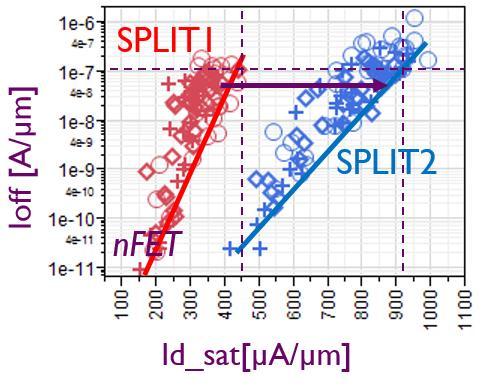
![ID[A] ID[A] imec bulk FinFET data Access to raw data and extracted FoM s Threshold](/docs-images/90/103079563/images/19-2.jpg "Voltage, Mismatch DC metrics and ID-VD, ID-VG characteristics FEOL/BEOL R/C and")

19 ID[A] ID[A] imec bulk FinFET data Access to raw data and extracted FoM s Threshold Voltage, Mismatch DC metrics and ID-VD, ID-VG characteristics FEOL/BEOL R/C and Ring-Oscillator circuits Full sweep data in VA Covers range of VG/VD and LG/nFin VG[V] Analog FoM, Reliability testing, ESD,... Available for subsequent model validation VG[V] VD[V]


20 30 Virtual Access Registered Users India Korea Singpr


21 New initiative: PhD Accelerator Prog. imec Reliability and failure mechanisms in advanced CMOS technologies 20 th -23 rd November places Outcome: Very successful + led to a number of enquiries CEA Leti Reliability & Defects in Advanced Technologies from Theory to practice 5 th -7 th March places Outcome: Tyndall National Institute Hands on nanoelectronics fabrication & characterisation 24 th -26 th April places


22 How to engage Please join us in this exciting opportunity for nanoelectronics research Any enquiries? Paul Sign up: Phone: Sign up and find out more online
ASCENT. European Nanoelectronics Infrastructure Access. Nicolás Cordero
 ASCENT European Nanoelectronics Infrastructure Access Nicolás Cordero The Challenge Cost/performance returns by scaling are diminishing Cost to achieve tape out on new nodes is increasing Technology Quarterly
Advanced PDK and Technologies accessible through ASCENT
 Advanced PDK and Technologies accessible through ASCENT MOS-AK Dresden, Sept. 3, 2018 L. Perniola*, O. Rozeau*, O. Faynot*, T. Poiroux*, P. Roseingrave^ olivier.faynot@cea.fr *Cea-Leti, Grenoble France;
ASCENT Open Access to 14nm PDKs T. Chiarella, N. Cordero, O. Faynot on behalf of the ASCENT teams
 ASCENT Open Access to 14nm PDKs T. Chiarella, N. Cordero, O. Faynot on behalf of the ASCENT teams chiarel@imec.be 11/09/2017 MOS AK Workshop @ ESSDERC 2017 Leuven, BE Content ASCENT in a nutshell Individual
research in the fields of nanoelectronics
 FRAUNHOFEr center Nanoelectronic Technologies research in the fields of nanoelectronics 1 contents Fraunhofer CNT in Profile 3 Competence Areas Analytics 4 Functional Electronic Materials 5 Device & Integration
write-nanocircuits Direct-write Jaebum Joo and Joseph M. Jacobson Molecular Machines, Media Lab Massachusetts Institute of Technology, Cambridge, MA
 Fab-in in-a-box: Direct-write write-nanocircuits Jaebum Joo and Joseph M. Jacobson Massachusetts Institute of Technology, Cambridge, MA April 17, 2008 Avogadro Scale Computing / 1 Avogadro number s? Intel
EUROSOI+- FP of 38 30/06/ FINAL PUBLISHABLE SUMMARY REPORT
 EUROSOI+- FP7-216373 3 of 38 30/06/2011 1. FINAL PUBLISHABLE SUMMARY REPORT EUROSOI+- FP7-216373 4 of 38 30/06/2011 EUROSOI+- FP7-216373 5 of 38 30/06/2011 The main and last objective of EUROSOI Network
Deliverable 4.2: TEM cross sections on prototyped Gated Resistors
 Deliverable 4.2: TEM cross sections on prototyped Gated Resistors Olga G. Varona, Geoff Walsh, Bernie Capraro Intel Ireland 21 June 2011 Abbreviation list D: drain FIB: focused ion-beam HRTEM: high resolution
Welcome to. A facility within the Nanometer Structure Consortium (nmc) at Lund University. nanolab. lund
 at Lund University. nanolab. lund") lund nanolab Welcome to A facility within the Nanometer Structure Consortium (nmc) at Lund University »It s a dream come true. This is the lab I always dreamt of. I didn t know it would ever exist.«ivan
lund nanolab Welcome to A facility within the Nanometer Structure Consortium (nmc) at Lund University »It s a dream come true. This is the lab I always dreamt of. I didn t know it would ever exist.«ivan
Introduction of New Products
 Field Emission Electron Microscope JEM-3100F For evaluation of materials in the fields of nanoscience and nanomaterials science, TEM is required to provide resolution and analytical capabilities that can
Nanotechnology, the infrastructure, and IBM s research projects
 Nanotechnology, the infrastructure, and IBM s research projects Dr. Paul Seidler Coordinator Nanotechnology Center, IBM Research - Zurich Nanotechnology is the understanding and control of matter at dimensions
Energy beam processing and the drive for ultra precision manufacturing
 Energy beam processing and the drive for ultra precision manufacturing An Exploration of Future Manufacturing Technologies in Response to the Increasing Demands and Complexity of Next Generation Smart
450mm and Moore s Law Advanced Packaging Challenges and the Impact of 3D
 450mm and Moore s Law Advanced Packaging Challenges and the Impact of 3D Doug Anberg VP, Technical Marketing Ultratech SOKUDO Lithography Breakfast Forum July 10, 2013 Agenda Next Generation Technology
Atomic-Level Control of the Thermoelectric Properties in Polytypoid Nanowires
 Atomic-Level Control of the Thermoelectric Properties in Polytypoid Nanowires Sean C. Andrews 1,2 *, Melissa A. Fardy 1,2 *, Michael C. Moore 1,2 *, Shaul Aloni 2, Minjuan Zhang 3, Velimir Radmilovic 2,4,
Full-screen mode Popup controls. Overview of the microscope user interface, TEM User Interface and TIA on the left and EDS on the right
 Quick Guide to Operating FEI Titan Themis G2 200 (S)TEM: TEM mode Susheng Tan Nanoscale Fabrication and Characterization Facility, University of Pittsburgh Office: M104/B01 Benedum Hall, 412-383-5978,
Course Outcome of M.Tech (VLSI Design)
") Course Outcome of M.Tech (VLSI Design) PVL108: Device Physics and Technology The students are able to: 1. Understand the basic physics of semiconductor devices and the basics theory of PN junction. 2.
Course Outcome of M.Tech (VLSI Design) PVL108: Device Physics and Technology The students are able to: 1. Understand the basic physics of semiconductor devices and the basics theory of PN junction. 2.
End-of-line Standard Substrates For the Characterization of organic
 FRAUNHOFER INSTITUTe FoR Photonic Microsystems IPMS End-of-line Standard Substrates For the Characterization of organic semiconductor Materials Over the last few years, organic electronics have become
Fabrication of Probes for High Resolution Optical Microscopy
 Fabrication of Probes for High Resolution Optical Microscopy Physics 564 Applied Optics Professor Andrès La Rosa David Logan May 27, 2010 Abstract Near Field Scanning Optical Microscopy (NSOM) is a technique
Collaboration: The Semiconductor Industry s Path to Survival and Growth
 Collaboration: The Semiconductor Industry s Path to Survival and Growth Dr. Michael R. Polcari President and CEO SEMATECH 15 March 2005 3/17/2005 J:\ADMCTR\OCE\M_Polcari\ITPC 10-04 1 Outline Environment
HOW TO CONTINUE COST SCALING. Hans Lebon
 HOW TO CONTINUE COST SCALING Hans Lebon OUTLINE Scaling & Scaling Challenges Imec Technology Roadmap Wafer size scaling : 450 mm 2 COST SCALING IMPROVED PERFORMANCE 3 GLOBAL TRAFFIC FORECAST Cloud Traffic
Reducing Transistor Variability For High Performance Low Power Chips
 Reducing Transistor Variability For High Performance Low Power Chips HOT Chips 24 Dr Robert Rogenmoser Senior Vice President Product Development & Engineering 1 HotChips 2012 Copyright 2011 SuVolta, Inc.
Appreciating the very little things: Status and future prospects of TEM at NUANCE
 Appreciating the very little things: Status and future prospects of TEM at NUANCE Dr. Roberto dos Reis roberto.reis@northwestern.edu 11/28/2018 Nature 542, pages75 79 (2017) TEM Facility Manager: Dr. Xiaobing
ECE 5745 Complex Digital ASIC Design Topic 2: CMOS Devices
 ECE 5745 Complex Digital ASIC Design Topic 2: CMOS Devices Christopher Batten School of Electrical and Computer Engineering Cornell University http://www.csl.cornell.edu/courses/ece5950 Simple Transistor
microelectronics services high-tech requires high-precision microelectronics services
 ELECTRICAL & ELECTRONICS microelectronics services high-tech requires high-precision microelectronics services WORLDWIDE Analysis, TESTING & CERTIFICATION LOCALLY AVAILABLE worldwide Electrical and electronic
Etch, Deposition, and Metrology Options for Cost-Effective Thin-Film Bulk Acoustic Resonator (FBAR) Production
 Production") Etch, Deposition, and Metrology Options for Cost-Effective Thin-Film Bulk Acoustic Resonator (FBAR) Production Figure 1 Veeco is driving System on a Chip Technology Frank M. Cumbo, Kurt E. Williams, John
Etch, Deposition, and Metrology Options for Cost-Effective Thin-Film Bulk Acoustic Resonator (FBAR) Production Figure 1 Veeco is driving System on a Chip Technology Frank M. Cumbo, Kurt E. Williams, John
How material engineering contributes to delivering innovation in the hyper connected world
 How material engineering contributes to delivering innovation in the hyper connected world Paul BOUDRE, Soitec CEO Leti Innovation Days - July 2018 Grenoble, France We live in a world of data In perpetual
Magellan XHR SEM. Discover the world of extreme high resolution scanning electron microscopy
 Magellan XHR SEM Discover the world of extreme high resolution scanning electron microscopy Gold particles on carbon test sample imaged at 200 V and a horizontal field width (HFW) of 500 nm. Unprecedented
Directional Growth of Ultra-long CsPbBr 3 Perovskite. Nanowires for High Performance Photodetectors
 Supporting information Directional Growth of Ultra-long CsPbBr 3 Perovskite Nanowires for High Performance Photodetectors Muhammad Shoaib, Xuehong Zhang, Xiaoxia Wang, Hong Zhou, Tao Xu, Xiao Wang, Xuelu
SUPPORTING INFORMATION
 SUPPORTING INFORMATION Surface-Guided CsPbBr 3 Perovskite Nanowires on Flat and Faceted Sapphire with Size-Dependent Photoluminescence and Fast Photoconductive Response Eitan Oksenberg, Ella Sanders, Ronit
Progress Energy Distinguished University Professor Jay Baliga. April 11, Acknowledgements
 Progress Energy Distinguished University Professor Jay Baliga April 11, 2019 Acknowledgements 1 Outline SiC Power MOSFET Breakthroughs achieved at NCSU PRESiCE: SiC Power Device Manufacturing Technology
4.1.2 InAs nanowire circuits fabricated by field-assisted selfassembly on a host substrate
 22 Annual Report 2010 - Solid-State Electronics Department 4.1.2 InAs nanowire circuits fabricated by field-assisted selfassembly on a host substrate Student Scientist in collaboration with R. Richter
Wafer-scale 3D integration of silicon-on-insulator RF amplifiers
 Wafer-scale integration of silicon-on-insulator RF amplifiers The MIT Faculty has made this article openly available. Please share how this access benefits you. Your story matters. Citation As Published
Development of JEM-2800 High Throughput Electron Microscope
 Development of JEM-2800 High Throughput Electron Microscope Mitsuhide Matsushita, Shuji Kawai, Takeshi Iwama, Katsuhiro Tanaka, Toshiko Kuba and Noriaki Endo EM Business Unit, JEOL Ltd. Electron Optics
Microscopic Structures
 Microscopic Structures Image Analysis Metal, 3D Image (Red-Green) The microscopic methods range from dark field / bright field microscopy through polarisation- and inverse microscopy to techniques like
A Brief Introduction to Single Electron Transistors. December 18, 2011
 A Brief Introduction to Single Electron Transistors Diogo AGUIAM OBRECZÁN Vince December 18, 2011 1 Abstract Transistor integration has come a long way since Moore s Law was first mentioned and current
Lecture: Integration of silicon photonics with electronics. Prepared by Jean-Marc FEDELI CEA-LETI
 Lecture: Integration of silicon photonics with electronics Prepared by Jean-Marc FEDELI CEA-LETI Context The goal is to give optical functionalities to electronics integrated circuit (EIC) The objectives
MAPPER: High throughput Maskless Lithography
 MAPPER: High throughput Maskless Lithography Marco Wieland CEA- Leti Alterative Lithography workshop 1 Today s agenda Introduction Applications Qualification of on-tool metrology by in-resist metrology
Silicon Photonics Technology Platform To Advance The Development Of Optical Interconnects
 Silicon Photonics Technology Platform To Advance The Development Of Optical Interconnects By Mieke Van Bavel, science editor, imec, Belgium; Joris Van Campenhout, imec, Belgium; Wim Bogaerts, imec s associated
Christian Boit TUB Berlin University of Technology Sect. Semiconductor Devices. 1
 Semiconductor Device & Analysis Center Berlin University of Technology Christian Boit TUB Berlin University of Technology Sect. Semiconductor Devices Christian.Boit@TU-Berlin.DE 1 Semiconductor Device
CMOL: Hybrid of CMOS with Overlaid Nanogrid and Nanodevice Structure. John Zacharkow
 CMOL: Hybrid of CMOS with Overlaid Nanogrid and Nanodevice Structure John Zacharkow Overview Introduction Background CMOS Review CMOL Breakdown Benefits/Shortcoming Looking into the Future Introduction
Micro-PackS, Technology Platform. Security Characterization Lab Opening
 September, 30 th 2008 Micro-PackS, Technology Platform Security Characterization Lab Opening Members : Micro-PackS in SCS cluster From Silicium to innovative & commucating device R&D structure, gathering
Test Structures Basics Part 1
 Test Structures Basics Part 1 By Christopher Henderson In this document we will provide an overview of test structures as they pertain to reliability. Test structures can provide critical insight into
Scanning electron microscope
 Scanning electron microscope 5 th CEMM workshop Maja Koblar, Sc. Eng. Physics Outline The basic principle? What is an electron? Parts of the SEM Electron gun Electromagnetic lenses Apertures Detectors
FinFET vs. FD-SOI Key Advantages & Disadvantages
 FinFET vs. FD-SOI Key Advantages & Disadvantages Amiad Conley Technical Marketing Manager Process Diagnostics & Control, Applied Materials ChipEx-2014, Apr 2014 1 Moore s Law The number of transistors
IN SITU BIASING & HEATING SOLUTIONS FOR TEM PLATFORMS
 IN SITU BIASING & HEATING SOLUTIONS FOR TEM PLATFORMS Solutions for In Situ Microscopy THE LIGHTNING SERIES LIGHTNING FEATURES Observe the real-time dynamics of materials under electrical and heating stimuli.
SUPPLEMENTARY INFORMATION
 In the format provided by the authors and unedited. Photon-triggered nanowire transistors Jungkil Kim, Hoo-Cheol Lee, Kyoung-Ho Kim, Min-Soo Hwang, Jin-Sung Park, Jung Min Lee, Jae-Pil So, Jae-Hyuck Choi,
Optimization of Threshold Voltage for 65nm PMOS Transistor using Silvaco TCAD Tools
 IOSR Journal of Electrical and Electronics Engineering (IOSR-JEEE) e-issn: 2278-1676,p-ISSN: 2320-3331, Volume 6, Issue 1 (May. - Jun. 2013), PP 62-67 Optimization of Threshold Voltage for 65nm PMOS Transistor
Jian-Wei Liu, Jing Zheng, Jin-Long Wang, Jie Xu, Hui-Hui Li, Shu-Hong Yu*
 Supporting Information Ultrathin 18 O 49 Nanowire Assemblies for Electrochromic Devices Jian-ei Liu, Jing Zheng, Jin-Long ang, Jie Xu, Hui-Hui Li, Shu-Hong Yu* Experimental Section Synthesis and Assembly
Micro Photonics, Berlin
 Imprint Nanopatterning Solution Platform for IndustRial assessment NANO IMPRINT LITHOGRAPHY (NIL) FOR PHOTONICS APPLICATIONS Hubert TEYSSEDRE Stefan LANDIS Sandra BOS Laurent PAIN Yannick LE TIEC LETI,
Instruction manual and data sheet ipca h
 1/15 instruction manual ipca-21-05-1000-800-h Instruction manual and data sheet ipca-21-05-1000-800-h Broad area interdigital photoconductive THz antenna with microlens array and hyperhemispherical silicon
EECS 151/251A Spring 2019 Digital Design and Integrated Circuits. Instructors: Wawrzynek. Lecture 8 EE141
 EECS 151/251A Spring 2019 Digital Design and Integrated Circuits Instructors: Wawrzynek Lecture 8 EE141 From the Bottom Up IC processing CMOS Circuits (next lecture) EE141 2 Overview of Physical Implementations
Enabling Breakthroughs In Technology
 Enabling Breakthroughs In Technology Mike Mayberry Director of Components Research VP, Technology and Manufacturing Group Intel Corporation June 2011 Defined To be defined Enabling a Steady Technology
Design of Analog CMOS Integrated Circuits
 Design of Analog CMOS Integrated Circuits Behzad Razavi Professor of Electrical Engineering University of California, Los Angeles H Boston Burr Ridge, IL Dubuque, IA Madison, WI New York San Francisco
Fin-Shaped Field Effect Transistor (FinFET) Min Ku Kim 03/07/2018
 Min Ku Kim 03/07/2018") Fin-Shaped Field Effect Transistor (FinFET) Min Ku Kim 03/07/2018 ECE 658 Sp 2018 Semiconductor Materials and Device Characterizations OUTLINE Background FinFET Future Roadmap Keeping up w/ Moore s Law
Fin-Shaped Field Effect Transistor (FinFET) Min Ku Kim 03/07/2018 ECE 658 Sp 2018 Semiconductor Materials and Device Characterizations OUTLINE Background FinFET Future Roadmap Keeping up w/ Moore s Law
DATASHEET CADENCE QRC EXTRACTION
 DATASHEET Cadence QRC Etraction, the industry s premier 3D fullchip parasitic etractor that is independent of design style or flow, is a fast and accurate RLCK etraction solution used during design implementation
Sub-micron technology IC fabrication process trends SOI technology. Development of CMOS technology. Technology problems due to scaling
 Goodbye Microelectronics Welcome Nanoelectronics Sub-micron technology IC fabrication process trends SOI technology SiGe Tranzistor in 50nm process Virus The thickness of gate oxide= 1.2 nm!!! Today we
DTU DANCHIP an open access micro/nanofabrication facility bridging academic research and small scale production
 DTU DANCHIP an open access micro/nanofabrication facility bridging academic research and small scale production DTU Danchip National Center for Micro- and Nanofabrication DTU Danchip DTU Danchip is Denmark
Quantum Devices and Integrated Circuits Based on Quantum Confinement in III-V Nanowire Networks Controlled by Nano-Schottky Gates
 ECS 2 Joint Intenational Meeting, San Francisco Sept. 2-7, 2 Sixth International Symposium on Quantum Confinement Quantum Devices and Integrated Circuits Based on Quantum Confinement in III-V Nanowire
The Reverberation of Successful Participation in European Cooperation Schemas
 The Reverberation of Successful Participation in European Cooperation Schemas Zora Střelcová Project Manager TESCAN Brno, s.r.o. zora.strelcova@tescan.cz HORIZON 2020 EUROPEAN UNION FUNDING FOR RESEARCH
1 FUNDAMENTAL CONCEPTS What is Noise Coupling 1
 Contents 1 FUNDAMENTAL CONCEPTS 1 1.1 What is Noise Coupling 1 1.2 Resistance 3 1.2.1 Resistivity and Resistance 3 1.2.2 Wire Resistance 4 1.2.3 Sheet Resistance 5 1.2.4 Skin Effect 6 1.2.5 Resistance
3-2-1 Contact: An Experimental Approach to the Analysis of Contacts in 45 nm and Below. Rasit Onur Topaloglu, Ph.D.
 3-2-1 Contact: An Experimental Approach to the Analysis of Contacts in 45 nm and Below Rasit Onur Topaloglu, Ph.D. Outline Introduction and Motivation Impact of Contact Resistance Test Structures for Contact
Issue 89 November 2016
 Voltage Contrast Part 1 By Christopher Henderson In this presentation, we discuss voltage contrast, one of a number of techniques that use scanning electron microscopy to aid in fault isolation. Voltage
The Cornell NanoScale Facility: NNCI Overview
 The Cornell NanoScale Facility: NNCI Overview Prof. Christopher Ober Lester B. Knight Director CNF: founded 1977 CNF Highlights 2017 is CNF s 40 th Anniversary as an NSF funded User Facility Using NNCI
Direct Observation of Current-Induced Motion of a. 3D Vortex Domain Wall in Cylindrical Nanowires
 Supporting Information Direct Observation of Current-Induced Motion of a 3D Vortex Domain Wall in Cylindrical Nanowires Yurii P. Ivanov,,, *, Andrey Chuvilin ǁ,, Sergey Lopatin, Hanan Mohammed, Jurgen
Basic Functional Analysis. Sample Report Richmond Road, Suite 500, Ottawa, ON K2H 5B7 Canada Tel:
 Basic Functional Analysis Sample Report 3685 Richmond Road, Suite 500, Ottawa, ON K2H 5B7 Canada Tel: 613-829-0414 www.chipworks.com Basic Functional Analysis Sample Report Some of the information in this
INTRODUCTION TO MOS TECHNOLOGY
 INTRODUCTION TO MOS TECHNOLOGY 1. The MOS transistor The most basic element in the design of a large scale integrated circuit is the transistor. For the processes we will discuss, the type of transistor
CS-TEM vs CS-STEM. FEI Titan CIME EPFL. Duncan Alexander EPFL-CIME
 CS-TEM vs CS-STEM Duncan Alexander EPFL-CIME 1 FEI Titan Themis @ CIME EPFL 60 300 kv Monochromator High brightness X-FEG Probe Cs-corrected: 0.7 Å @ 300 kv Image Cs-corrected: 0.7 Å @ 300 kv Super-X EDX
New Process Technologies Will silicon CMOS carry us to the end of the Roadmap?
 HPEC Workshop 2006 New Process Technologies Will silicon CMOS carry us to the end of the Roadmap? Craig L. Keast, Chenson Chen, Mike Fritze, Jakub Kedzierski, Dave Shaver HPEC 2006-1 Outline A brief history
Scientific Highlights 2016
 Scientific Highlights 2016 Science and Technology Sector Schools and Faculties Faculty of Science Louvain School of Engineering (EPL) Faculty of Architecture, Architectural Engineering and Urban Planning
Inspection-analysis Solutions for High-quality and High-efficiency Semiconductor Device Manufacturing
 Hitachi Review Vol. 52 (2003), No. 3 125 Inspection-analysis Solutions for High-quality and High-efficiency Semiconductor Device Manufacturing Kenji Watanabe, Dr. Eng. Aritoshi Sugimoto Mari Nozoe OVERVIEW:
STM RH-ASIC capability
 STM RH-ASIC capability JAXA 24 th MicroElectronic Workshop 13 th 14 th October 2011 Prepared by STM Crolles and AeroSpace Unit Deep Sub Micron (DSM) is strategic for Europe Strategic importance of European
MYUNGHWAN PARK Westchester Park Drive, APT 1510, College Park, Maryland MOBILE : (+1) ,
 ,") RESEARCH INTERESTS MYUNGHWAN PARK 6200 Westchester Park Drive, APT 1510, College Park, Maryland 20740 MOBILE : (+1) 240-678-9863, EMAIL : mhpark@umd.edu My overall research interest is the physics of integrated
RESEARCH INTERESTS MYUNGHWAN PARK 6200 Westchester Park Drive, APT 1510, College Park, Maryland 20740 MOBILE : (+1) 240-678-9863, EMAIL : mhpark@umd.edu My overall research interest is the physics of integrated
Nanowire Transistors. Physics of Devices and Materials in One Dimension
 Nanowire Transistors Physics of Devices and Materials in One Dimension From quantum mechanical concepts to practical circuit applications, this book presents a self-contained and up-to-date account of
Scanning electron microscope
 Scanning electron microscope 6 th CEMM workshop Maja Koblar, Sc. Eng. Physics Outline The basic principle? What is an electron? Parts of the SEM Electron gun Electromagnetic lenses Apertures Chamber and
Transparent p-type SnO Nanowires with Unprecedented Hole Mobility among Oxide Semiconductors
 Supplementary Information Transparent p-type SnO Nanowires with Unprecedented Hole Mobility among Oxide Semiconductors J. A. Caraveo-Frescas and H. N. Alshareef* Materials Science and Engineering, King
Dual-channel Lock-in Amplifier Module
 Dual-channel Lock-in Amplifier Module Introduction Phase-locked amplification and demodulation techniques of weak signals have a wide range of applications in Turnable Diode Laser Absorption Spectrum (TDLAS)
Supporting Information. Single-Nanowire Electrochemical Probe Detection for Internally Optimized Mechanism of
 Supporting Information Single-Nanowire Electrochemical Probe Detection for Internally Optimized Mechanism of Porous Graphene in Electrochemical Devices Ping Hu, Mengyu Yan, Xuanpeng Wang, Chunhua Han,*
SiNANO-NEREID Workshop:
 SiNANO-NEREID Workshop: Towards a new NanoElectronics Roadmap for Europe Leuven, September 11 th, 2017 WP3/Task 3.2 Connectivity RF and mmw Design Outline Connectivity, what connectivity? High data rates
Consumer Electronics: from chip to system
 Consumer Electronics: from chip to system Kees Revenberg Co-founder/MD June 6 th 2018 APC, University of Warwick, UK NMI Techworks 6-6-2018 CONTENT Introduction Consumer Electronics Definition Trends and
RESEARCH FAB MICROELECTRONICS GERMANY (FMD) The Virtual Institute for Combined Microelectronic Research and Development
 The Virtual Institute for Combined Microelectronic Research and Development") RESEARCH FAB MICROELECTRONICS GERMANY (FMD) The Virtual Institute for Combined Microelectronic Research and Development Mircoelectronic development trends Micro- and Nanoelectronics are key enabling technologies
RESEARCH FAB MICROELECTRONICS GERMANY (FMD) The Virtual Institute for Combined Microelectronic Research and Development Mircoelectronic development trends Micro- and Nanoelectronics are key enabling technologies
Raman Spectroscopy and Transmission Electron Microscopy of Si x Ge 1-x -Ge-Si Core-Double-Shell Nanowires
 Raman Spectroscopy and Transmission Electron Microscopy of Si x Ge 1-x -Ge-Si Core-Double-Shell Nanowires Paola Perez Mentor: Feng Wen PI: Emanuel Tutuc Background One-dimensional semiconducting nanowires
CHA2098b RoHS COMPLIANT
 CHA98b RoHS COMPLIANT -4GHz High Gain Buffer Amplifier GaAs Monolithic Microwave IC Description Vd1 Vd2,3 The CHA98b is a high gain broadband threestage monolithic buffer amplifier. It is designed for
Laser patterning and projection lithography
 Introduction to Nanofabrication Techniques: Laser patterning and projection lithography Benjamin Johnston Macquarie University David O Connor Bandwidth Foundry - USYD The OptoFab node of ANFF Broad ranging
Module 4B7: VLSI Design, Technology, and CAD. Scanning Electron Microscopical Examination of CMOS Integrated Circuit
 Engineering Tripos Part IIB FOURTH YEAR Module 4B7: VLSI Design, Technology, and CAD Laboratory Experiment Dr D Holburn and Mr B Breton Scanning Electron Microscopical Examination of CMOS Integrated Circuit
Alternatives to standard MOSFETs. What problems are we really trying to solve?
 Alternatives to standard MOSFETs A number of alternative FET schemes have been proposed, with an eye toward scaling up to the 10 nm node. Modifications to the standard MOSFET include: Silicon-in-insulator
Design & Simulation of Multi Gate Piezoelectric FET Devices for Sensing Applications
 Design & Simulation of Multi Gate Piezoelectric FET Devices for Sensing Applications Sunita Malik 1, Manoj Kumar Duhan 2 Electronics & Communication Engineering Department, Deenbandhu Chhotu Ram University
2. Pulsed Acoustic Microscopy and Picosecond Ultrasonics
 1st International Symposium on Laser Ultrasonics: Science, Technology and Applications July 16-18 2008, Montreal, Canada Picosecond Ultrasonic Microscopy of Semiconductor Nanostructures Thomas J GRIMSLEY
The Department of Advanced Materials Engineering. Materials and Processes in Polymeric Microelectronics
 The Department of Advanced Materials Engineering Materials and Processes in Polymeric Microelectronics 1 Outline Materials and Processes in Polymeric Microelectronics Polymeric Microelectronics Process
JEM-F200. Multi-purpose Electron Microscope. Scientific / Metrology Instruments Multi-purpose Electron Microscope
 Scientific / Metrology Instruments Multi-purpose Electron Microscope JEM-F200 Multi-purpose Electron Microscope JEM-F200/F2 is a multi-purpose electron microscope of the new generation to meet today's
Lecture 4. The CMOS Inverter. DC Transfer Curve: Load line. DC Operation: Voltage Transfer Characteristic. Noise in Digital Integrated Circuits
 Noise in Digital Integrated Circuits Lecture 4 The CMOS Inverter i(t) v(t) V DD Peter Cheung Department of Electrical & Electronic Engineering Imperial College London URL: www.ee.ic.ac.uk/pcheung/ E-mail:
photolithographic techniques (1). Molybdenum electrodes (50 nm thick) are deposited by
. Molybdenum electrodes (50 nm thick) are deposited by") Supporting online material Materials and Methods Single-walled carbon nanotube (SWNT) devices are fabricated using standard photolithographic techniques (1). Molybdenum electrodes (50 nm thick) are deposited
Supporting online material Materials and Methods Single-walled carbon nanotube (SWNT) devices are fabricated using standard photolithographic techniques (1). Molybdenum electrodes (50 nm thick) are deposited
*Corresponding author.
 Supporting Information for: Ligand-Free, Quantum-Confined Cs 2 SnI 6 Perovskite Nanocrystals Dmitriy S. Dolzhnikov, Chen Wang, Yadong Xu, Mercouri G. Kanatzidis, and Emily A. Weiss * Department of Chemistry,
Dual Metal Gate and Conventional MOSFET at Sub nm for Analog Application
 Dual Metal Gate and Conventional MOSFET at Sub nm for Analog Application Sonal Aggarwal 1 and Rajbir Singh 2 1 Department of Electronic Science, Kurukshetra university,kurukshetra sonal.aggarwal88@gmail.com
45nm Foundry CMOS with Mask-Lite Reduced Mask Costs
 This work is sponsored by the Air Force Research Laboratory (AFRL/RVSE) TPOC: Mr. Kenneth Hebert 45nm Foundry CMOS with Mask-Lite Reduced Mask Costs 25 October 2011 www.americansemi.com 2011 American Semiconductor,
Opportunities and Challenges for Nanoelectronic Devices and Processes
 The Sixth U.S.-Korea Forum on Nanotechnology, April 28-29, 2009, Las Vegas, NV Opportunities and Challenges for Nanoelectronic Devices and Processes Yoshio Nishi Professor, Electrical Engineering, Material
Low Voltage Electron Microscope
 LVEM5 Low Voltage Electron Microscope Nanoscale from your benchtop LVEM5 Delong America DELONG INSTRUMENTS COMPACT BUT POWERFUL The LVEM5 is designed to excel across a broad range of applications in material
Recent Developments in Multifunctional Integration. Stephan Guttowski, Head of Technology Park»Heterointegration«, Fraunhofer FMD
 Recent Developments in Multifunctional Integration Stephan Guttowski, Head of Technology Park»Heterointegration«, Fraunhofer FMD Founding Participants 2 One-Stop-Shop for developments from wafer technologies
77 GHz VCO for Car Radar Systems T625_VCO2_W Preliminary Data Sheet
 77 GHz VCO for Car Radar Systems Preliminary Data Sheet Operating Frequency: 76-77 GHz Tuning Range > 1 GHz Output matched to 50 Ω Application in Car Radar Systems ESD: Electrostatic discharge sensitive
Semiconductor Process Reliability SVTW 2012 Esko Mikkola, Ph.D. & Andrew Levy
 Semiconductor Process Reliability SVTW 2012 Esko Mikkola, Ph.D. & Andrew Levy 1 IC Failure Modes Affecting Reliability Via/metallization failure mechanisms Electro migration Stress migration Transistor
FOUNDRY SERVICE. SEI's FEATURE. Wireless Devices FOUNDRY SERVICE. SRD-800DD, SRD-500DD D-FET Process Lg=0.8, 0.5µm. Ion Implanted MESFETs SRD-301ED
 FOUNDRY SERVICE 01.04. Foundry services have been one of the core businesses at SEI, providing sophisticated GaAs IC technology for all customers. SEI offers very flexible service to support the customers