The Cornell NanoScale Facility: NNCI Overview
|
|
|
- Linette Summers
- 5 years ago
- Views:
Transcription
1 The Cornell NanoScale Facility: NNCI Overview Prof. Christopher Ober Lester B. Knight Director CNF: founded 1977
2 CNF Highlights 2017 is CNF s 40 th Anniversary as an NSF funded User Facility Using NNCI definitions: 53% Non-traditional 23 (20.7 FTE) scientific and technical staff - (+4 admin) provide on-site user support (~4000 training sessions/year) 15 NNCI Technical Experts among staff First meeting of external advisory board
3 CNF Highlights 2017 is CNF s 40 th Anniversary as an NSF funded User Facility Using NNCI definitions: 53% Non-traditional 23 (20.7 FTE) scientific and technical staff - (+4 admin) provide on-site user support (~4000 training sessions/year) 15 NNCI Technical Experts among staff First meeting of external advisory board
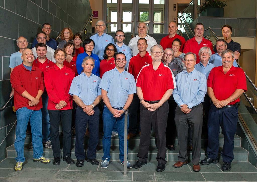
4 CNF Staff
5 External Advisory Board Bob Celotta, NIST (Chair) Chuck Black, BNL Alice White, Boston University Advisory board met this past November Steve Turner PacBiosystems
 Strong Local Emphasis: Silicon Photonics Magnetic")
, PARADIM (MIP), CHESS 468 years of Staff Tech Experience Success commercializing research (17/12)")
6 Key Technologies and Experience Advanced Lithography: 3 Steppers, EBL -> JEOL 9500, JEOL 6300 In-House mask making Plasma Processing (17 plasma etchers) Strong Local Emphasis: Silicon Photonics Magnetic Materials Fluidics-> Life Sciences; NanoAg MEMS, NEMS 2-D Materials Proximity to other NSF centers: CCMR (MRSEC), PARADIM (MIP), CHESS 468 years of Staff Tech Experience Success commercializing research (17/12) JEOL 9500

 for growth and deposition Comprehensive set of etching tools (~16)")
 Atomic Layer")
7 CNF Equipment Resources Equipment highlights (> 120 major tools): 2 state-of the-art electron-beam lithography systems. DUV Stepper, i-line, g-line, contact and proximity photolithography. In-house mask making capabilities. 5 hot-process banks (20 tubes) for growth and deposition Comprehensive set of etching tools (~16) including DSE, ICP etchers Plasma Enhanced deposition High resolution SEMs, AFM, Optical Metrology Chemical Mechanical Polishing Ion Implantation Molecular Vapor Deposition (SAMs) Atomic Layer Deposition Materials Ink Jet Printing 3D Printing NanoImprint Lithography and Hot Embossing
 at the full 4-inch wafer")

8 2-D Electronic Materials The Park group at Cornell University successfully demonstrated batch fabrication of high performance field-effect transistors from monolayer molybdenum disulfide (MoS 2 ) at the full 4-inch wafer scale. Transfer of the monolayer films allows multi-level fabrication of vertically stacked transistor devices for three-dimensional circuitry. This work is a step towards the realization of atomically-thin integrated circuitry.


9 Listening to the Brain with a Transistor In Nature Communications Khodagholy et al from NYU and Ecole des Mines reported recording the electrical activity of a large number of neurons providing a pathway to understand the brain and its information-processing capabilities. Such neural recordings are used in clinics for diagnosis in patients with epilepsy and brain tumors, and to help paralyzed people control prosthetic limbs. A solution to the challenges of probing these signals is to use a biocompatible and flexible organic transistor as the recording device. This transistor, which operates in a manner similar to that found in microprocessors, amplifies the signal while recording it. As a result, recordings show a 10 fold improvement in signal quality. c d Flexible organic brain probe(a) with integrated amplifier (b) implanted in a rat brain(c) used to record (d) a bicuculline-induced epileptiform spike from a transistor (pink), a surface electrode (blue) and penetrating electrodes (black).


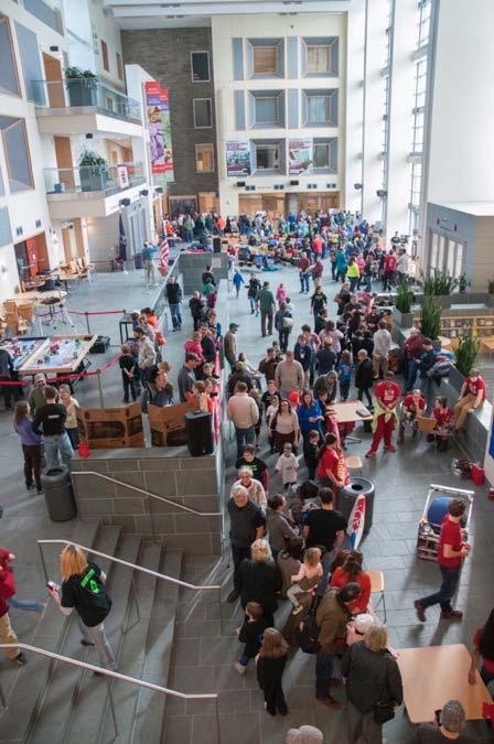
10 Outreach & Workforce Training CNF Fellows and Ambassadors Technology and Characterization at the NanoScale Short Course held in January and June Going on this week. NNCI Intranetwork Plasma Processing Workshop GenISys Workshop for users & staff Annual Symposium held in September REU program 5 interns, 10 weeks; mini convocation held jointly with PARADIM interns Revised Promotional Brochures Produced 20 Nanonuggets for NNCO 10-9 NanoDay
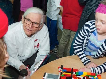
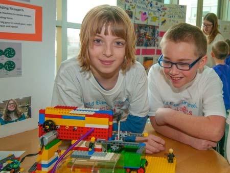

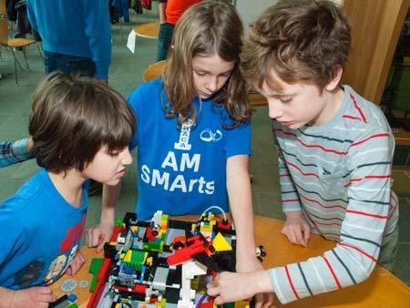
11 Educational Outreach - LEGO Annual 1 Day Event brings ~ 20 teams of elementary school age participants


 and")

12 4H 2 Events Annually: 4H Leaders Program (Cornell is NYS HQ) and Career Exploration Program (HS age groups)


13 REU Rapidly spun up program for 5 Interns Combined some events with PARADIM REU to reach critical mass Organized a miniconvocation Rathbun successful IRES grant to initiate ireu sent 5 past REUs to Japan


14 Disney NSF Award supplement to Update Exhibit
15 Partnerships & Commercialization Company News: 1 New Start up Esper Biosciences 2 Small Company applicants for FuzeHub Manufacturing Innovation Grants 1 StartUp CNF Award NYS program 2 Commercialization Foundry Partners Key Partnerships: JEOL electron beam lithography GenISys CAD Oxford Instruments Plasma Processing & ALD Suss Alta Spray, SCIL PARADIM NSF funded material innovation platform, a materials user facility

")

16 Research to Commercialization -energy harvester chip MicroGen Systems, is designing and manufacturing nanotechnology/microelectromechanical Systems micro-power and micro-sensor products for wireless sensor and mobile electronics. MicroGen developed its baseline piezoelectric vibrational energy harvester (PZEH) technology at the Cornell NanoScale Facility and is now manufacturing its platform technology at the X-FAB foundry in Germany. Output voltage OCV > 10 Volts, and output power Pload f1 and 0.1 G Where f1 is Hz
DTU DANCHIP an open access micro/nanofabrication facility bridging academic research and small scale production
 DTU DANCHIP an open access micro/nanofabrication facility bridging academic research and small scale production DTU Danchip National Center for Micro- and Nanofabrication DTU Danchip DTU Danchip is Denmark
A Perspective on Semiconductor Equipment. R. B. Herring March 4, 2004
 A Perspective on Semiconductor Equipment R. B. Herring March 4, 2004 Outline Semiconductor Industry Overview of circuit fabrication Semiconductor Equipment Industry Some equipment business strategies Product
NanoFabrication Kingston. Seminar and Webinar January 31, 2017 Rob Knobel Associate Professor, Dept. of Physics Queen s University
 NanoFabrication Kingston Seminar and Webinar January 31, 2017 Rob Knobel Associate Professor, Dept. of Physics Queen s University What is NFK? It s a place, an team of experts and a service. The goal of
Nanostencil Lithography and Nanoelectronic Applications
 Microsystems Laboratory Nanostencil Lithography and Nanoelectronic Applications Oscar Vazquez, Marc van den Boogaart, Dr. Lianne Doeswijk, Prof. Juergen Brugger, LMIS1 Dr. Chan Woo Park, Visiting Professor
Major Fabrication Steps in MOS Process Flow
 Major Fabrication Steps in MOS Process Flow UV light Mask oxygen Silicon dioxide photoresist exposed photoresist oxide Silicon substrate Oxidation (Field oxide) Photoresist Coating Mask-Wafer Alignment
write-nanocircuits Direct-write Jaebum Joo and Joseph M. Jacobson Molecular Machines, Media Lab Massachusetts Institute of Technology, Cambridge, MA
 Fab-in in-a-box: Direct-write write-nanocircuits Jaebum Joo and Joseph M. Jacobson Massachusetts Institute of Technology, Cambridge, MA April 17, 2008 Avogadro Scale Computing / 1 Avogadro number s? Intel
Semiconductor Manufacturing Technology. Semiconductor Manufacturing Technology. Photolithography: Resist Development and Advanced Lithography
 Semiconductor Manufacturing Technology Michael Quirk & Julian Serda October 2001 by Prentice Hall Chapter 15 Photolithography: Resist Development and Advanced Lithography Eight Basic Steps of Photolithography
32nm High-K/Metal Gate Version Including 2nd Generation Intel Core processor family
 From Sand to Silicon Making of a Chip Illustrations 32nm High-K/Metal Gate Version Including 2nd Generation Intel Core processor family April 2011 1 The illustrations on the following foils are low resolution
Design of MEMS Piezoelectric Vibrational Energy Harvesters for Industrial and Commercial Applications
 Design of MEMS Piezoelectric Vibrational Energy Harvesters for Industrial and Commercial Applications Consumer Applications Civil Infrastructure Kathleen M. Vaeth, Vice President of Engineering microgen
The Department of Advanced Materials Engineering. Materials and Processes in Polymeric Microelectronics
 The Department of Advanced Materials Engineering Materials and Processes in Polymeric Microelectronics 1 Outline Materials and Processes in Polymeric Microelectronics Polymeric Microelectronics Process
Micro-PackS, Technology Platform. Security Characterization Lab Opening
 September, 30 th 2008 Micro-PackS, Technology Platform Security Characterization Lab Opening Members : Micro-PackS in SCS cluster From Silicium to innovative & commucating device R&D structure, gathering
Micro-Nanofabrication
 Zheng Cui Micro-Nanofabrication TECHNOLOGIES AND APPLICATIONS ^f**"?* ö Springer Higher Education Press -T O Table of Content Preface About the Author Chapter 1 Introduction 1 1.1 Micro-nanotechnologies
NNCI Computation. Azad Naeemi Georgia Institute of Technology
 NNCI Computation Azad Naeemi Georgia Institute of Technology azad@gatech.edu Modeling and Simulation Modeling and simulation can enhance nanoscale fabrication and characterization: guide experimental research
GLOBAL MARKETS, TECHNOLOGIES AND MATERIALS FOR THIN AND ULTRATHIN FILMS
 GLOBAL MARKETS, TECHNOLOGIES AND MATERIALS FOR THIN AND ULTRATHIN FILMS SMC057C August Margareth Gagliardi Project Analyst ISBN: 1-62296-338-5 BCC Research 49 Walnut Park, Building 2 Wellesley, MA 02481
Holst Centre Wireless Autonomous Sensor Technologies & Flexible Electronics
 February 10, 2011 Holst Centre Wireless Autonomous Sensor Technologies & Flexible Electronics Presentation overview -General overview -Research focus < 4 Holst Centre: a solid partner in research Independent,
Nanomanufacturing and Fabrication By Matthew Margolis
 Nanomanufacturing and Fabrication By Matthew Margolis Manufacturing is the transformation of raw materials into finished goods for sale, or intermediate processes involving the production or finishing
ASCENT Overview. European Nanoelectronics Infrastructure Access. MOS-AK Workshop, Infineon, Munich, 13 th March 2018.
 ASCENT Overview MOS-AK Workshop, Infineon, Munich, 13 th March 2018 European Nanoelectronics Infrastructure Access Paul Roseingrave The Challenge Cost/performance returns by scaling are diminishing Cost
Introduction to Microdevices and Microsystems
 PHYS 534 (Fall 2008) Module on Microsystems & Microfabrication Lecture 1 Introduction to Microdevices and Microsystems Srikar Vengallatore, McGill University 1 Introduction to Microsystems Outline of Lecture
University of Minnesota Nano Fabrication Center Standard Operating Procedure Equipment Name:
 Equipment Name: Coral Name: Nanoimprinter Revision Number: 1.1 Model: NX-B200 Revisionist: M. Fisher Location: Bay 4 Date: 2/12/2010 1 Description Nanonex NX-B200 nanoimprinter is another method of transfer
Photolithography I ( Part 1 )
") 1 Photolithography I ( Part 1 ) Chapter 13 : Semiconductor Manufacturing Technology by M. Quirk & J. Serda Bjørn-Ove Fimland, Department of Electronics and Telecommunication, Norwegian University of Science
1 Photolithography I ( Part 1 ) Chapter 13 : Semiconductor Manufacturing Technology by M. Quirk & J. Serda Bjørn-Ove Fimland, Department of Electronics and Telecommunication, Norwegian University of Science
research in the fields of nanoelectronics
 FRAUNHOFEr center Nanoelectronic Technologies research in the fields of nanoelectronics 1 contents Fraunhofer CNT in Profile 3 Competence Areas Analytics 4 Functional Electronic Materials 5 Device & Integration
IC1301 -WiPE. Wireless Power Transmission for Sustainable Electronics. SWG4.1: Space Applications. 25 March 2014
 IC1301 -WiPE Wireless Power Transmission for Sustainable Electronics SWG4.1: Space Applications 25 March 2014 Alexandru Takacs CNRS LAAS, Toulouse, France University of Toulouse III Paul Sabatier, France
Technology for the MEMS processing and testing environment. SUSS MicroTec AG Dr. Hans-Georg Kapitza
 Technology for the MEMS processing and testing environment SUSS MicroTec AG Dr. Hans-Georg Kapitza 1 SUSS MicroTec Industrial Group Founded 1949 as Karl Süss KG GmbH&Co. in Garching/ Munich San Jose Waterbury
the world leader in metrology of piezoelectrics expanding into new areas!
 aixacct Systems GmbH Talbotstr. 25 52068 Aachen Germany Phone: +49 (0) 241-47 57 03 0 Fax: +49 (0) 241-47 57 03 66 www.aixacct.com info@aixacct.com Welcome to aixacct Systems, the world leader in metrology
Des MEMS aux NEMS : évolution des technologies et des concepts aux travers des développements menés au LETI
 Des MEMS aux NEMS : évolution des technologies et des concepts aux travers des développements menés au LETI Ph. Robert 1 Content LETI at a glance From MEMS to NEMS: 30 years of technological evolution
FABRICATION OF CMOS INTEGRATED CIRCUITS. Dr. Mohammed M. Farag
 FABRICATION OF CMOS INTEGRATED CIRCUITS Dr. Mohammed M. Farag Outline Overview of CMOS Fabrication Processes The CMOS Fabrication Process Flow Design Rules Reference: Uyemura, John P. "Introduction to
SAMPLE SLIDES & COURSE OUTLINE. Core Competency In Semiconductor Technology: 2. FABRICATION. Dr. Theodore (Ted) Dellin
 Dellin") & Digging Deeper Devices, Fabrication & Reliability For More Info:.com or email Dellin@ieee.org SAMPLE SLIDES & COURSE OUTLINE In : 2. A Easy, Effective, of How Devices Are.. Recommended for everyone who
& Digging Deeper Devices, Fabrication & Reliability For More Info:.com or email Dellin@ieee.org SAMPLE SLIDES & COURSE OUTLINE In : 2. A Easy, Effective, of How Devices Are.. Recommended for everyone who
University of California, Berkeley Department of Mechanical Engineering. ME 290R Topics in Manufacturing, Fall 2014: Lithography
 University of California, Berkeley Department of Mechanical Engineering ME 290R Topics in Manufacturing, Fall 2014: Lithography Class meetings: TuTh 3.30 5pm in 1165 Etcheverry Tentative class schedule
Etch, Deposition, and Metrology Options for Cost-Effective Thin-Film Bulk Acoustic Resonator (FBAR) Production
 Production") Etch, Deposition, and Metrology Options for Cost-Effective Thin-Film Bulk Acoustic Resonator (FBAR) Production Figure 1 Veeco is driving System on a Chip Technology Frank M. Cumbo, Kurt E. Williams, John
Etch, Deposition, and Metrology Options for Cost-Effective Thin-Film Bulk Acoustic Resonator (FBAR) Production Figure 1 Veeco is driving System on a Chip Technology Frank M. Cumbo, Kurt E. Williams, John
All-Glass Gray Scale PhotoMasks Enable New Technologies. Che-Kuang (Chuck) Wu Canyon Materials, Inc.
 Wu Canyon Materials, Inc.") All-Glass Gray Scale PhotoMasks Enable New Technologies Che-Kuang (Chuck) Wu Canyon Materials, Inc. 1 Overview All-Glass Gray Scale Photomask technologies include: HEBS-glasses and LDW-glasses HEBS-glass
All-Glass Gray Scale PhotoMasks Enable New Technologies Che-Kuang (Chuck) Wu Canyon Materials, Inc. 1 Overview All-Glass Gray Scale Photomask technologies include: HEBS-glasses and LDW-glasses HEBS-glass
CMOS Digital Integrated Circuits Lec 2 Fabrication of MOSFETs
 CMOS Digital Integrated Circuits Lec 2 Fabrication of MOSFETs 1 CMOS Digital Integrated Circuits 3 rd Edition Categories of Materials Materials can be categorized into three main groups regarding their
EE 410: Integrated Circuit Fabrication Laboratory
 EE 410: Integrated Circuit Fabrication Laboratory 1 EE 410: Integrated Circuit Fabrication Laboratory Web Site: Instructor: http://www.stanford.edu/class/ee410 https://ccnet.stanford.edu/ee410/ (on CCNET)
PROFILE CONTROL OF A BOROSILICATE-GLASS GROOVE FORMED BY DEEP REACTIVE ION ETCHING. Teruhisa Akashi and Yasuhiro Yoshimura
 Stresa, Italy, 25-27 April 2007 PROFILE CONTROL OF A BOROSILICATE-GLASS GROOVE FORMED BY DEEP REACTIVE ION ETCHING Teruhisa Akashi and Yasuhiro Yoshimura Mechanical Engineering Research Laboratory (MERL),
Feature-level Compensation & Control
 Feature-level Compensation & Control 2 Sensors and Control Nathan Cheung, Kameshwar Poolla, Costas Spanos Workshop 11/19/2003 3 Metrology, Control, and Integration Nathan Cheung, UCB SOI Wafers Multi wavelength
Heterogeneous Technology Alliance. SOI MEMS Platform
 Heterogeneous Technology Alliance SOI MEMS Platform Added value of HTA SOI MEMS Platform to customers 23-Aug-11 Page 1 Attractive offering of HTA SOI MEMS Platform One-stop shop 1 Very extensive R&D resources,
Welcome to. A facility within the Nanometer Structure Consortium (nmc) at Lund University. nanolab. lund
 at Lund University. nanolab. lund") lund nanolab Welcome to A facility within the Nanometer Structure Consortium (nmc) at Lund University »It s a dream come true. This is the lab I always dreamt of. I didn t know it would ever exist.«ivan
lund nanolab Welcome to A facility within the Nanometer Structure Consortium (nmc) at Lund University »It s a dream come true. This is the lab I always dreamt of. I didn t know it would ever exist.«ivan
Fault Diagnosis Algorithms Part 2
 Fault Diagnosis Algorithms Part 2 By Christopher Henderson Page 1 Fault Diagnosis Algorithms Part 2 Page 5 Technical Tidbit Page 8 Ask the Experts Figure 4. Circuit schematic. This is an example of a circuit
Fabricating 2.5D, 3D, 5.5D Devices
 Fabricating 2.5D, 3D, 5.5D Devices Bob Patti, CTO rpatti@tezzaron.com Tezzar on Semiconduct or 04/15/2013 1 Gen4 Dis-Integrated 3D Memory DRAM layers 42nm node 2 million vertical connections per lay per
1 Introduction 1.1 HISTORICAL DEVELOPMENT OF MICROELECTRONICS
 1 Introduction 1.1 HISTORICAL DEVELOPMENT OF MICROELECTRONICS The field of microelectronics began in 1948 when the first transistor was invented. This first transistor was a point-contact transistor, which
Part 5-1: Lithography
 Part 5-1: Lithography Yao-Joe Yang 1 Pattern Transfer (Patterning) Types of lithography systems: Optical X-ray electron beam writer (non-traditional, no masks) Two-dimensional pattern transfer: limited
Technology transfer and business development for innovation projects. From local market to global industry.
 Technology transfer and business development for innovation projects. From local market to global industry. www.zntc.ru Well positioned for innovative business development Fab и Lab R&D Multifunctional
Smart Vision Chip Fabricated Using Three Dimensional Integration Technology
 Smart Vision Chip Fabricated Using Three Dimensional Integration Technology H.Kurino, M.Nakagawa, K.W.Lee, T.Nakamura, Y.Yamada, K.T.Park and M.Koyanagi Dept. of Machine Intelligence and Systems Engineering,
Noel Technologies. Provider of Advanced Lithography and Semiconductor Thin Film Services
 Noel Technologies Provider of Advanced Lithography and Semiconductor Thin Film Services Noel Technologies Keith Best Biography Over the last 27 years, Keith Best has held a variety of semiconductor processing
Scientific Highlights 2016
 Scientific Highlights 2016 Science and Technology Sector Schools and Faculties Faculty of Science Louvain School of Engineering (EPL) Faculty of Architecture, Architectural Engineering and Urban Planning
System100Pro. Production tools for wafer processing. The Business of Science
 System100Pro Production tools for wafer processing The Business of Science Process tools & modules Oxford Instruments' System100Pro production tools are built on 200 mm, 300 mm and multiwafer batch process
From Sand to Silicon Making of a Chip Illustrations May 2009
 From Sand to Silicon Making of a Chip Illustrations May 2009 1 The illustrations on the following foils are low resolution images that visually support the explanations of the individual steps. For publishing
Pattern Transfer CD-AFM. Resist Features on Poly. Poly Features on Oxide. Quate Group, Stanford University
 Resist Features on Poly Pattern Transfer Poly Features on Oxide CD-AFM The Critical Dimension AFM Boot -Shaped Tip Tip shape is optimized to sense topography on vertical surfaces Two-dimensional feedback
Semiconductor Manufacturing and Inspection Technologies for the 0.1 µm Process Generation
 Hitachi Review Vol. 49 (2000), No. 4 199 Semiconductor Manufacturing and Inspection Technologies for the 0.1 µm Process Generation Takafumi Tokunaga Katsutaka Kimura Jun Nakazato Masaki Nagao, D. Eng.
Lithography Session. EUV Lithography optics current status and outlook. F. Roozeboom Professor TU Eindhoven & TNO-Holst Centre, Eindhoven, Netherlands
 Lithography Session F. Roozeboom Professor TU Eindhoven & TNO-Holst Centre, Eindhoven, Netherlands Fred Roozeboom is a Professor at Eindhoven University of Technology, The Netherlands and Senior Technical
Front to Back Alignment and Metrology Performance for Advanced Packaging
 Lithography Session F. Roozeboom Professor TU Eindhoven & TNO-Holst Centre, Eindhoven, Netherlands Fred Roozeboom is a Professor at Eindhoven University of Technology, The Netherlands and Senior Technical
Nanofluidic Diodes based on Nanotube Heterojunctions
 Supporting Information Nanofluidic Diodes based on Nanotube Heterojunctions Ruoxue Yan, Wenjie Liang, Rong Fan, Peidong Yang 1 Department of Chemistry, University of California, Berkeley, CA 94720, USA
State-of-the-art device fabrication techniques
 State-of-the-art device fabrication techniques! Standard Photo-lithography and e-beam lithography! Advanced lithography techniques used in semiconductor industry Deposition: Thermal evaporation, e-gun
G450C. Global 450mm Consortium at CNSE. Michael Liehr, General Manager G450C, Vice President for Research
 Global 450mm Consortium at CNSE Michael Liehr, General Manager G450C, Vice President for Research - CNSE Overview - G450C Vision - G450C Mission - Org Structure - Scope - Timeline The Road Ahead for Nano-Fabrication
1.1 PHILOSOPHY OF MICRO/NANOFABRICATION
 CHAPTER Introduction 1 C H A P T E R C O N T E N T S 1.1 Philosophy of Micro/Nanofabrication... 1 1.2 The Industry Science Dualism... 5 1.3 Industrial Applications... 8 1.4 Purpose and Organization of
Photolithography Technology and Application
 Photolithography Technology and Application Jeff Tsai Director, Graduate Institute of Electro-Optical Engineering Tatung University Art or Science? Lind width = 100 to 5 micron meter!! Resolution = ~ 3
IWORID J. Schmitz page 1. Wafer-level CMOS post-processing Jurriaan Schmitz
 IWORID J. Schmitz page 1 Wafer-level CMOS post-processing Jurriaan Schmitz IWORID J. Schmitz page 2 Outline Introduction on wafer-level post-proc. CMOS: a smart, but fragile substrate Post-processing steps
Large Area, Flexible Electronics TWG. Chair: Dan Gamota, Jabil
 Large Area, Flexible Electronics TWG Chair: Dan Gamota, Jabil Large Area Flexible Electronics Roadmap History 09/2005 inemi Stakeholders identify Flexible Electronics as Future Growth Market and authorize
Lecture 7. Lithography and Pattern Transfer. Reading: Chapter 7
 Lecture 7 Lithography and Pattern Transfer Reading: Chapter 7 Used for Pattern transfer into oxides, metals, semiconductors. 3 types of Photoresists (PR): Lithography and Photoresists 1.) Positive: PR
Yoshihiko ISOBE Hiroshi MUTO Tsuyoshi FUKADA Seiji FUJINO
 Yoshihiko ISOBE Hiroshi MUTO Tsuyoshi FUKADA Seiji FUJINO Increased performance requirements in terms of the environment, safety and comfort have recently been imposed on automobiles to ensure efficient
Characterization of Silicon-based Ultrasonic Nozzles
 Tamkang Journal of Science and Engineering, Vol. 7, No. 2, pp. 123 127 (24) 123 Characterization of licon-based Ultrasonic Nozzles Y. L. Song 1,2 *, S. C. Tsai 1,3, Y. F. Chou 4, W. J. Chen 1, T. K. Tseng
Triple i - The key to your success
 Triple i - The key to your success The needs and challenges of today s world are becoming ever more demanding. Standards are constantly rising. Creativity, reliability and high performance are basic prerequisites
Institute of Solid State Physics. Technische Universität Graz. Lithography. Peter Hadley
 Technische Universität Graz Institute of Solid State Physics Lithography Peter Hadley http://www.cleanroom.byu.edu/virtual_cleanroom.parts/lithography.html http://www.cleanroom.byu.edu/su8.phtml Spin coater
SUNY Poly in a New Era
 SUNY Poly in a New Era Bahgat Sammakia Interim President, SUNY Polytechnic Institute SUNY Poly in a New Era Overview SUNY Poly is recognized as a global leader in advanced electronics Research and Development,
Projects and Partners Working with Chalcogenide Advanced Manufacturing Partnership (ChAMP)
") Projects and Partners Working with Chalcogenide Advanced Manufacturing Partnership (ChAMP) Dr John Lincoln Industrial Liaison Officer j.lincoln@soton.ac.uk March 2015 ChAMP Aims Establish world leading
Projects and Partners Working with Chalcogenide Advanced Manufacturing Partnership (ChAMP) Dr John Lincoln Industrial Liaison Officer j.lincoln@soton.ac.uk March 2015 ChAMP Aims Establish world leading
Module 11: Photolithography. Lecture 14: Photolithography 4 (Continued)
") Module 11: Photolithography Lecture 14: Photolithography 4 (Continued) 1 In the previous lecture, we have discussed the utility of the three printing modes, and their relative advantages and disadvantages.
Module 11: Photolithography Lecture 14: Photolithography 4 (Continued) 1 In the previous lecture, we have discussed the utility of the three printing modes, and their relative advantages and disadvantages.
Manufacturing Development of a New Electroplated Magnetic Alloy Enabling Commercialization of PwrSoC Products
 Manufacturing Development of a New Electroplated Magnetic Alloy Enabling Commercialization of PwrSoC Products Trifon Liakopoulos, Amrit Panda, Matt Wilkowski and Ashraf Lotfi PowerSoC 2012 CONTENTS Definitions
CHAPTER 2 POLARIZATION SPLITTER- ROTATOR BASED ON A DOUBLE- ETCHED DIRECTIONAL COUPLER
 CHAPTER 2 POLARIZATION SPLITTER- ROTATOR BASED ON A DOUBLE- ETCHED DIRECTIONAL COUPLER As we discussed in chapter 1, silicon photonics has received much attention in the last decade. The main reason is
Course Outcome of M.Tech (VLSI Design)
") Course Outcome of M.Tech (VLSI Design) PVL108: Device Physics and Technology The students are able to: 1. Understand the basic physics of semiconductor devices and the basics theory of PN junction. 2.
Course Outcome of M.Tech (VLSI Design) PVL108: Device Physics and Technology The students are able to: 1. Understand the basic physics of semiconductor devices and the basics theory of PN junction. 2.
AC : EXPERIMENTAL MODULES INTRODUCING MICRO- FABRICATION UTILIZING A MULTIDISCIPLINARY APPROACH
 AC 2011-1595: EXPERIMENTAL MODULES INTRODUCING MICRO- FABRICATION UTILIZING A MULTIDISCIPLINARY APPROACH Shawn Wagoner, Binghamton University Director, Nanofabrication Labatory at Binghamton University,
EQUIPMENT TRAINING LOG
 EQUIPMENT TRAINING LOG Name: Start Date: Email: Cell / Phone #: PI: PI Phone#: Signature of Trainer Date After Hours Access Depositions Tools CHA Mack 50 Evaporation (superuser tool) E-Beam 1 evaporation
Graphene electro-optic modulator with 30 GHz bandwidth
 Graphene electro-optic modulator with 30 GHz bandwidth Christopher T. Phare 1, Yoon-Ho Daniel Lee 1, Jaime Cardenas 1, and Michal Lipson 1,2,* 1School of Electrical and Computer Engineering, Cornell University,
Market and technology trends in advanced packaging
 Close Market and technology trends in advanced packaging Executive OVERVIEW Recent advances in device miniaturization trends have placed stringent requirements for all aspects of product manufacturing.
Nanoscale Material Characterization with Differential Interferometric Atomic Force Microscopy
 Nanoscale Material Characterization with Differential Interferometric Atomic Force Microscopy F. Sarioglu, M. Liu, K. Vijayraghavan, A. Gellineau, O. Solgaard E. L. Ginzton Laboratory University Tip-sample
FOUNDRY SERVICE. SEI's FEATURE. Wireless Devices FOUNDRY SERVICE. SRD-800DD, SRD-500DD D-FET Process Lg=0.8, 0.5µm. Ion Implanted MESFETs SRD-301ED
 FOUNDRY SERVICE 01.04. Foundry services have been one of the core businesses at SEI, providing sophisticated GaAs IC technology for all customers. SEI offers very flexible service to support the customers
Energy & Space. International Presentations
 Energy & Space International Presentations 2012-2013 Advanced Electronics 3D Printed Circuit Boards 3D Printed Circuit Boards for Solder-Free Printable Electronics 4x4 Vehicles Arduino WiFi Android Controllers
microelectronics services high-tech requires high-precision microelectronics services
 ELECTRICAL & ELECTRONICS microelectronics services high-tech requires high-precision microelectronics services WORLDWIDE Analysis, TESTING & CERTIFICATION LOCALLY AVAILABLE worldwide Electrical and electronic
SILICON BASED CAPACITIVE SENSORS FOR VIBRATION CONTROL
 SILICON BASED CAPACITIVE SENSORS FOR VIBRATION CONTROL Shailesh Kumar, A.K Meena, Monika Chaudhary & Amita Gupta* Solid State Physics Laboratory, Timarpur, Delhi-110054, India *Email: amita_gupta/sspl@ssplnet.org
MICROFLEX Project: MEMS on New Emerging Smart Textiles/Flexibles
 MICROFLEX Project: MEMS on New Emerging Smart Textiles/Flexibles S Beeby, M J Tudor, R Torah, K Yang, Y Wei Dr Steve Beeby ESD Research Group Smart Fabrics 2011 5 th April 2011 Overview Introduce the MicroFlex
Nanomanufacturing and Fabrication
 Nanomanufacturing and Fabrication Matthew Margolis http://www.cnm.es/im b/pages/services/im ages/nanofabrication%20laboratory_archivos/im age007.jpg What we will cover! Definitions! Top Down Vs Bottom
Atomic-layer deposition of ultrathin gate dielectrics and Si new functional devices
 Atomic-layer deposition of ultrathin gate dielectrics and Si new functional devices Anri Nakajima Research Center for Nanodevices and Systems, Hiroshima University 1-4-2 Kagamiyama, Higashi-Hiroshima,
A Laser-Based Thin-Film Growth Monitor
 TECHNOLOGY by Charles Taylor, Darryl Barlett, Eric Chason, and Jerry Floro A Laser-Based Thin-Film Growth Monitor The Multi-beam Optical Sensor (MOS) was developed jointly by k-space Associates (Ann Arbor,
Lithographic Performance and Mix-and-Match Lithography using 100 kv Electron Beam System JBX-9300FS
 Lithographic Performance and Mix-and-Match Lithography using 100 kv Electron Beam System JBX-9300FS Yukinori Ochiai, Takashi Ogura, Mitsuru Narihiro, and Kohichi Arai Silicon Systems Research Laboratories,
photolithographic techniques (1). Molybdenum electrodes (50 nm thick) are deposited by
. Molybdenum electrodes (50 nm thick) are deposited by") Supporting online material Materials and Methods Single-walled carbon nanotube (SWNT) devices are fabricated using standard photolithographic techniques (1). Molybdenum electrodes (50 nm thick) are deposited
Supporting online material Materials and Methods Single-walled carbon nanotube (SWNT) devices are fabricated using standard photolithographic techniques (1). Molybdenum electrodes (50 nm thick) are deposited
ME 434 MEMS Tuning Fork Gyroscope Amanda Bristow Stephen Nary Travis Barton 12/9/10
 ME 434 MEMS Tuning Fork Gyroscope Amanda Bristow Stephen Nary Travis Barton 12/9/10 1 Abstract MEMS based gyroscopes have gained in popularity for use as rotation rate sensors in commercial products like
MICRO YAW RATE SENSORS
 1 MICRO YAW RATE SENSORS FIELD OF THE INVENTION This invention relates to micro yaw rate sensors suitable for measuring yaw rate around its sensing axis. More particularly, to micro yaw rate sensors fabricated
Transistor was first invented by William.B.Shockley, Walter Brattain and John Bardeen of Bell Labratories. In 1961, first IC was introduced.
 Unit 1 Basic MOS Technology Transistor was first invented by William.B.Shockley, Walter Brattain and John Bardeen of Bell Labratories. In 1961, first IC was introduced. Levels of Integration:- i) SSI:-
EUV Lithography Transition from Research to Commercialization
 EUV Lithography Transition from Research to Commercialization Charles W. Gwyn and Peter J. Silverman and Intel Corporation Photomask Japan 2003 Pacifico Yokohama, Kanagawa, Japan Gwyn:PMJ:4/17/03:1 EUV
SUPPLEMENTARY INFORMATION
 Vertical nanowire electrode arrays as a scalable platform for intracellular interfacing to neuronal circuits Jacob T. Robinson, 1* Marsela Jorgolli, 2* Alex K. Shalek, 1 Myung-Han Yoon, 1 Rona S. Gertner,
Nanotechnology, the infrastructure, and IBM s research projects
 Nanotechnology, the infrastructure, and IBM s research projects Dr. Paul Seidler Coordinator Nanotechnology Center, IBM Research - Zurich Nanotechnology is the understanding and control of matter at dimensions
UW WNF Washington Nanofabrication Facility Annual Report Page i
 UW WNF Washington Nanofabrication Facility Annual Report 2015-2016 Page i Front cover: WNF staff engineer Albert Bailey and Associate Director Michael Khbeis inspect the construction of the new lithography
Semiconductor Process Diagnosis and Prognosis for DSfM
 Semiconductor Process Diagnosis and Prognosis for DSfM Department of Electronic Engineering Prof. Sang Jeen Hong Nov. 19, 2014 1/2 Agenda 1. Semiconductor Manufacturing Industry 2. Roles of Semiconductor
450mm and Moore s Law Advanced Packaging Challenges and the Impact of 3D
 450mm and Moore s Law Advanced Packaging Challenges and the Impact of 3D Doug Anberg VP, Technical Marketing Ultratech SOKUDO Lithography Breakfast Forum July 10, 2013 Agenda Next Generation Technology
Micro- and Nano- Fabrication and Replication Techniques
 Micro- and Nano- Fabrication and Replication Techniques Why do we have to write thing small and replicate fast? Plenty of Room at the Bottom Richard P. Feynman, December 1959 How do we write it? We have
Presented by: V.Lakshana Regd. No.: Information Technology CET, Bhubaneswar
 BRAIN COMPUTER INTERFACE Presented by: V.Lakshana Regd. No.: 0601106040 Information Technology CET, Bhubaneswar Brain Computer Interface from fiction to reality... In the futuristic vision of the Wachowski
End-of-line Standard Substrates For the Characterization of organic
 FRAUNHOFER INSTITUTe FoR Photonic Microsystems IPMS End-of-line Standard Substrates For the Characterization of organic semiconductor Materials Over the last few years, organic electronics have become
EE4800 CMOS Digital IC Design & Analysis. Lecture 1 Introduction Zhuo Feng
 EE4800 CMOS Digital IC Design & Analysis Lecture 1 Introduction Zhuo Feng 1.1 Prof. Zhuo Feng Office: EERC 730 Phone: 487-3116 Email: zhuofeng@mtu.edu Class Website http://www.ece.mtu.edu/~zhuofeng/ee4800fall2010.html
420 Intro to VLSI Design
 Dept of Electrical and Computer Engineering 420 Intro to VLSI Design Lecture 0: Course Introduction and Overview Valencia M. Joyner Spring 2005 Getting Started Syllabus About the Instructor Labs, Problem
Advanced PDK and Technologies accessible through ASCENT
 Advanced PDK and Technologies accessible through ASCENT MOS-AK Dresden, Sept. 3, 2018 L. Perniola*, O. Rozeau*, O. Faynot*, T. Poiroux*, P. Roseingrave^ olivier.faynot@cea.fr *Cea-Leti, Grenoble France;
Deliverable D5.2 DEMO chip processing option 3
 Deliverable D5.2 DEMO chip processing option 3 Deliverable D5.2 DEMO chip processing Option 3 Date: 22-03-2017 PiezoMAT 2017-03-22_Delivrable_D5.2 Author(s): E.Saoutieff; M.Allain (CEA) Participant(s):