Introduction to Microdevices and Microsystems
|
|
|
- Jonathan Lane
- 5 years ago
- Views:
Transcription
1 PHYS 534 (Fall 2008) Module on Microsystems & Microfabrication Lecture 1 Introduction to Microdevices and Microsystems Srikar Vengallatore, McGill University 1 Introduction to Microsystems Outline of Lecture -Basic definitions and examples -How are they designed? -How are they manufactured? 2 1
2 Introduction to Microsystems Micro: Small Input System Output System dimensions: 1 mm to 10 cm Structural components: 10 nm to 100 μm Designed and manufactured to perform useful activity 3 LENGTH SCALES Bacteria Molecules Atoms 10-3 m = 1 mm 10-4 m = 100 μm 10-5 m = 10 μm 10-6 m = 1 μm 10-7 m = 100 nm 10-8 m = 10 nm 10-9 m = 1 nm STRUCTURES FOR MICROSYSTEMS m = 0.1 nm 4 2


3 1 m 1 mm 1 μm 1 nm Source: Kalpakjian and Schmid 5 Example 1. Integrated Circuit >1 Million wires per cm 2! No moving parts $200 Billion per year Revolutionary (Internet, computers, ) (I.B.M) 6 3


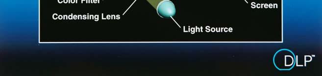
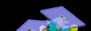
4 Cross-Section of an I.B.M Integrated Circuit Copper Silicon dioxide 1 μm Silicon Tungsten 7 Example 2: Texas Instruments Micromirrors 1 μm DIGITAL LIGHT PROCESSING (DLP) 8 4


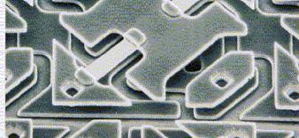
5 9 Electron Micrograph of Texas Instruments DMD Torsional Hinge


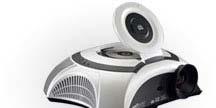
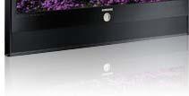

6 Samsung DLP TVs DLP Projectors
 Microsystems")
 Power")
7 13 Some Terminology Microsystems are known by many names.. Microdevices Microelectronics Microelectromechanical i l Systems (MEMS) Microsystems Technology (MST) Microfluidic systems Micro total analysis systems (micro-tas) Bio-MEMS/ Bio-microsystems Optical-MEMS/ Optical microsystems RF-MEMS (for radio-frequency MEMS) Power MEMS (micro-engines, micro fuel cells) 14 7


8 Terminology Reflects Evolution of Technology In the beginning, there was the transistor.. Invented in 1947 in Bell Labs. Nothing micro yet! 15 Walter Brattain John Bardeen William Shockley Nobel Prize in Physics (1956) 16 8

 Robert")
9 Use of a Transistor in an Electrical Circuit Jack Kilby, Texas Instruments 17 The World s First Integrated Circuit Aluminum Wires (Interconnects) Robert Noyce 18 9
 Robert Noyce (co-founder")
")

 1992")
 2000 10 8")
10 Kilby: Nobel Prize for Physics (2000) Robert Noyce (co-founder of Intel) 19 Evolution of Integrated Circuits ( ) Year 1960 < 100 # of Transistors per device (4004, 8008) (386 processor) (486 processor) x10 6 (Pentium processor) (Pentium II) (Pentium 4) 20 10


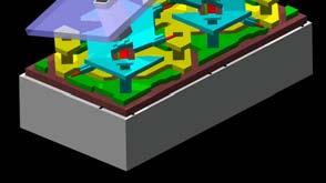
11 Stage 2: From Microelectronics to Micromechanics 1970s: Realization that mechanical components can also be miniaturized Emergence of micromachined pressure sensors Sealed Vacuum Cavity Membrane Pressure Port (P) 21 Pressure Sensors: Principle of Operation Estimate pressure by measuring deflection 8 mm 22 11


12 Micromachined Pressure Sensors are now Widely Used s: Micro Sensors and Actuators Sensors for force, acceleration, pressure, mass,. Micromachined Accelerometers Analog Devices ~8 million accelerometers are manufactured each year 24 12

13 Principle of Operation of Accelerometer k m F = ma kδ a = a F = kδ m δ Quasi-Static Accelerometer 25 Applications for Micromachined Accelerometers Modal analysis of vibratory systems Navigation Crash Sensors: Air-bag deployment in automobiles Protection of hard-disks in laptop computers Video games
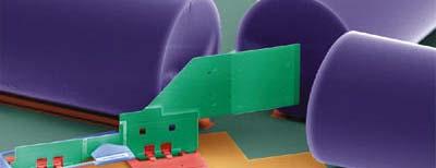
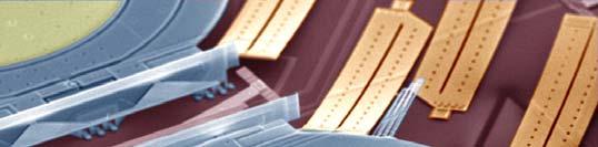
14 1980s Micro Actuators: Motion in Microsystems ELECTROSTATIC ACTUATORS Linear Spring, k Mass, m Gap, g 0 + V _ g < g 0 Fixed electrode Micro Electro + Mechanical System, or MEMS 27 Types of Microscale Actuators Electrostatic Thermal Piezoelectric Shape Memory Alloy Motion is either due to Applied Forces or Differential Expansion and Contraction 28 14
15 THERMAL ACTUATORS α 1 α 2 α 1 > α 2 Heat s: Increasing Focus on Commercialization Important Trends Microsystem community focused on Utility (design, manufacture, marketing, reliability, cost, etc.) Range expanded from Electro + Mechanical to multiple energy domains Optical Chemical Radio-Frequency communications Biological Fluidic There is a complete world of engineering at these scales! 30 15


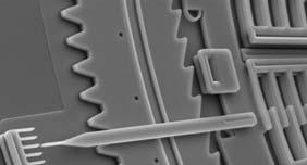
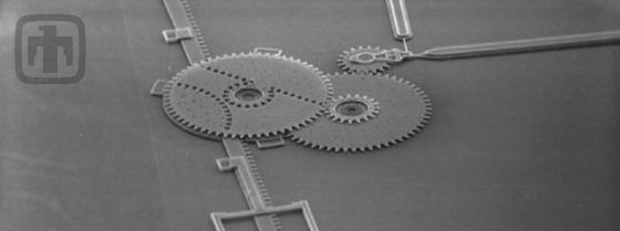
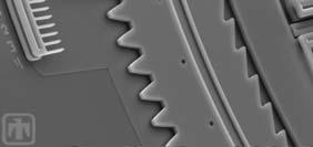
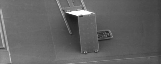
16 OPTICAL MICROSYSTEMS FOR DISPLAYS Silicon Light Machines 31 OPTICAL MICROSYSTEMS FOR COMMUNICATIONS 32 16
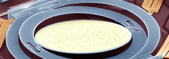
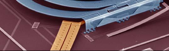

17 OPTICAL CROSS-CONNECTS Lucent 33 OPTICAL MICROSYSTEMS FOR SENSING POLYCHROMATOR 10 μm 34 17


18 1990s: Microfluidics and Bio-Microsystems Texas Instruments D. Therriault, Ecole Polytechnique 35 Microfluidic Networks 36 18


19 1990s: Micro Needles for Painless Drug Delivery Georgia Institute of Technology 37 IMPLANTABLE CHIPS FOR PROGRAMMED DRUG DELIVERY 38 19


20 Microchips 39 EMERGING APPLICATIONS: PORTABLE POWER GENERATION Direct Methanol Fuel cell Toshiba V for 5 hours with one cartridge No recharge times 40 20


")
 Cathode")

21 Micro Gas Turbine Engine MIT 41 Micro Solid-Oxide Fuel Cells Anode (NiO-YSZ) Électrolyte (YSZ) Cathode (LSM) McGill University/ Ecole Polytechnique 42 21
22 Refining our Terminology In this course, we will use MICROSYSTEMS as a synonym for Microdevices Microelectronics Microelectromechanical Systems (MEMS) Microsystems Technology (MST) Microfluidic systems Micro total analysis systems (micro-tas) Bio-MEMS/ Bio-microsystems Optical-MEMS/ Optical microsystems RF-MEMS (for radio-frequency MEMS) Power MEMS (micro-engines, micro fuel cells) 43 Microsystems are useful. Computation Information storage & display Optical telecommunications Sensing (force, mass, acceleration, chemistry, biology,.) Actuator technology Portable power generation Energy storage Microscale chemical synthesis and analysis Medical diagnostics Therapeutics (drug delivery)
23 Estimated Global Market for Microsystems Device Applications Market Integrated Information & >$250 Billion Circuits Communications Ink-Jet Nozzles Accelerometers Pressure Sensors DNA Microarrays Printers Automobiles Genome sequencing ~$10 billion Drug delivery, fuel cells, microneedles, etc. (in advanced stages of commercialization) 45 Outline of Lecture Introduction to Microsystems -Basic definitions and examples -How are they designed? -How are they manufactured? 46 23


24 47 How are they Designed? Formulate a plan to satisfy a need or solve a problem*. If this plan results in the creation of something having a physical reality, then the product must be: -Functional -Safe -Reliable -Competitive -Usable -Manufacturable -Marketable *JE Shigley, CR Mischke & RG Budynas, Mechanical Engineering Design 48 24
25 Ashby s Approach to Design Market need Creativity & experience Concept Evaluation of competition Manufacturing considerations Embodiment Behavioral models In-house expertise Detail Management decisions Product Specification 49 Modeling and Analysis of Microsystems Microsystems operate in multiple energy domains (mechanical, fluidic, electrostatic, thermal, magnetic, ) Frequently, coupling between different domains (electromechanical; thermoelastic; magnetomechanical,..) Critical question: validity of continuum physics 50 25
26 Approach to Structural Design What kind of STRUCTURES (Machine elements) to use? Beams, plates, rods, or membranes? Solid section or shaped cross-section? Monolithic or composite? Electrostatic or electrothermal actuation? What kind of MATERIALS to use? Ceramics, metals, or polymers? Fiber-reinforced composites or layered composites? Structural Design is Constrained by Manufacturing Limitations 51 How are they manufactured? Starting Material Flat Plate (substrate; wafer) Add material Remove Material Pattern transfer (Photolithography) Package microdevice! 52 26
27 Overview of Microdevice Manufacture Starting Material: Substrate (wafer) Subtractive Processes Wet etching Dry etching Plasma etching DRIE Polishing Processes Patterning Additive Processes Photolithography E-beam lithography Ion beam lithography Soft lithography Evaporation Sputtering CVD Electrodeposition Wafer bonding Package Microdevice 53 Catalog of Manufacturing Processes Patterning Techniques: Photolithography, Microstamping, Electron/ion beam lithography, Soft lithography, Additive processes: Thin-film deposition, wafer bonding, oxidation, epitaxy,.. Subtractive processes: Wet etching, dry etching, ion milling, deep reactive ion etching, We will study these processes in GREAT DETAIL! 54 27
?")


28 Where are they Made (Fabricated)? Need Clean Room Fabrication Facilities (Fabs) Micromachining = Microfabrication = Microdevice Manufacture

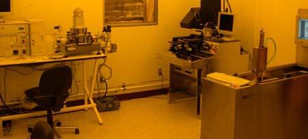
29 NanoTools Microfabrication Facility at McGill University Basement of the Rutherford Physics Building 57 Images courtesy of Sandia National Laboratories 58 29


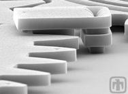
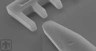
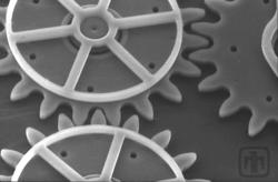
30 Fundamentally Different Approach to Manufacturing Parallel manufacture of hundreds of devices Simultaneous manufacture & assembly of components Layer-by-layer manufacture 10 6 mirrors 6x10 6 moving parts 59 Objective of this Module: Manufacturing of Microsystems This is an area of very active research Focus on: Fundamental principles + Established methods Science lags behind technology (We will use it even if we don t understand why it works!) Learn ideas, but also some crucial details Learn by assimilation: Case Studies 60 30
31 Market Need MECH 553: Design and Manufacture of Microdevices System concept Device concept Structural Embodiment Design Requirements Structural Embodiment Process Constraints Details Microdevice Additive Processes (Thin film deposition) Processes Pattern formation (Photolithography) Subtractive processes (Etching) 61 31
MEMS in ECE at CMU. Gary K. Fedder
 MEMS in ECE at CMU Gary K. Fedder Department of Electrical and Computer Engineering and The Robotics Institute Carnegie Mellon University Pittsburgh, PA 15213-3890 fedder@ece.cmu.edu http://www.ece.cmu.edu/~mems
The Department of Advanced Materials Engineering. Materials and Processes in Polymeric Microelectronics
 The Department of Advanced Materials Engineering Materials and Processes in Polymeric Microelectronics 1 Outline Materials and Processes in Polymeric Microelectronics Polymeric Microelectronics Process
RF MEMS Simulation High Isolation CPW Shunt Switches
 RF MEMS Simulation High Isolation CPW Shunt Switches Authored by: Desmond Tan James Chow Ansoft Corporation Ansoft 2003 / Global Seminars: Delivering Performance Presentation #4 What s MEMS Micro-Electro-Mechanical
TUTORIAL on the Industrialization of MEMS
 Munich Germany 11-13 September 2007 TUTORIAL on the Industrialization of MEMS Date: Monday, September 10 th, 2007 Venue: Organizer: TU München, Main Campus, Arcisstrasse 21, 80333 München Werner Weber,
Reducing MEMS product development and commercialization time
 Reducing MEMS product development and commercialization time Introduction Fariborz Maseeh, Andrew Swiecki, Nora Finch IntelliSense Corporation 36 Jonspin Road, Wilmington MA 01887 www.intellisense.com
1 Introduction 1.1 HISTORICAL DEVELOPMENT OF MICROELECTRONICS
 1 Introduction 1.1 HISTORICAL DEVELOPMENT OF MICROELECTRONICS The field of microelectronics began in 1948 when the first transistor was invented. This first transistor was a point-contact transistor, which
EE C245 ME C218 Introduction to MEMS Design
 EE C245 ME C218 Introduction to MEMS Design Fall 2008 Prof. Clark T.-C. Nguyen Dept. of Electrical Engineering & Computer Sciences University of California at Berkeley Berkeley, CA 94720 Lecture 1: Definition
EE C245 ME C218 Introduction to MEMS Design Fall 2007
 EE C245 ME C218 Introduction to MEMS Design Fall 2007 Prof. Clark T.-C. Nguyen Dept. of Electrical Engineering & Computer Sciences University of California at Berkeley Berkeley, CA 94720 Lecture 1: Definition
Chapter 1, Introduction
 Introduction to Semiconductor Manufacturing Technology Chapter 1, Introduction hxiao89@hotmail.com 1 Objective After taking this course, you will able to Use common semiconductor terminology Describe a
Progress due to: Feature size reduction - 0.7X/3 years (Moore s Law). Increasing chip size - 16% per year. Creativity in implementing functions.
. Increasing chip size - 16% per year. Creativity in implementing functions.") Introduction - Chapter 1 Evolution of IC Fabrication 1960 and 1990 integrated t circuits. it Progress due to: Feature size reduction - 0.7X/3 years (Moore s Law). Increasing chip size - 16% per year. Creativity
Introduction - Chapter 1 Evolution of IC Fabrication 1960 and 1990 integrated t circuits. it Progress due to: Feature size reduction - 0.7X/3 years (Moore s Law). Increasing chip size - 16% per year. Creativity
Academic Course Description SRM University Faculty of Engineering and Technology Department of Electronics and Communication Engineering
 Academic Course Description SRM University Faculty of Engineering and Technology Department of Electronics and Communication Engineering EC0032 Introduction to MEMS Eighth semester, 2014-15 (Even Semester)
VLSI Design. Introduction
 Tassadaq Hussain VLSI Design Introduction Outcome of this course Problem Aims Objectives Outcomes Data Collection Theoretical Model Mathematical Model Validate Development Analysis and Observation Pseudo
MEMS Sensors: From Automotive. CE Applications. MicroNanoTec Forum Innovations for Industry April 19 th Hannover, Germany
 MEMS Sensors: From Automotive to CE Applications MicroNanoTec Forum Innovations for Industry 2010 April 19 th Hannover, Germany Oliver Schatz, CTO 1 Engineering April 2010 GmbH 2009. All rights reserved,
EE C245 ME C218 Introduction to MEMS Design Fall 2010
 Instructor: Prof. Clark T.-C. Nguyen EE C245 ME C218 Introduction to MEMS Design Fall 2010 Prof. Clark T.-C. Nguyen Dept. of Electrical Engineering & Computer Sciences University of California at Berkeley
Transistor was first invented by William.B.Shockley, Walter Brattain and John Bardeen of Bell Labratories. In 1961, first IC was introduced.
 Unit 1 Basic MOS Technology Transistor was first invented by William.B.Shockley, Walter Brattain and John Bardeen of Bell Labratories. In 1961, first IC was introduced. Levels of Integration:- i) SSI:-
Industrialization of Micro-Electro-Mechanical Systems. Werner Weber Infineon Technologies
 Industrialization of Micro-Electro-Mechanical Systems Werner Weber Infineon Technologies Semiconductor-based MEMS market MEMS Market 2004 (total 22.7 BUS$) Others mostly Digital Light Projection IR Sensors
VLSI Design. Introduction
 VLSI Design Introduction Outline Introduction Silicon, pn-junctions and transistors A Brief History Operation of MOS Transistors CMOS circuits Fabrication steps for CMOS circuits Introduction Integrated
Faculty Development Program on Micro-Electro-Mechanical Systems (MEMS Sensor)
") Faculty Development Program on Micro-Electro-Mechanical Systems (MEMS Report MEMS sensors have been dominating the consumer products such as mobile phones, music players and other portable devices. With
Faculty Development Program on Micro-Electro-Mechanical Systems (MEMS Report MEMS sensors have been dominating the consumer products such as mobile phones, music players and other portable devices. With
High-yield Fabrication Methods for MEMS Tilt Mirror Array for Optical Switches
 : MEMS Device Technologies High-yield Fabrication Methods for MEMS Tilt Mirror Array for Optical Switches Joji Yamaguchi, Tomomi Sakata, Nobuhiro Shimoyama, Hiromu Ishii, Fusao Shimokawa, and Tsuyoshi
An X band RF MEMS switch based on silicon-on-glass architecture
 Sādhanā Vol. 34, Part 4, August 2009, pp. 625 631. Printed in India An X band RF MEMS switch based on silicon-on-glass architecture M S GIRIDHAR, ASHWINI JAMBHALIKAR, J JOHN, R ISLAM, C L NAGENDRA and
AC : EXPERIMENTAL MODULES INTRODUCING MICRO- FABRICATION UTILIZING A MULTIDISCIPLINARY APPROACH
 AC 2011-1595: EXPERIMENTAL MODULES INTRODUCING MICRO- FABRICATION UTILIZING A MULTIDISCIPLINARY APPROACH Shawn Wagoner, Binghamton University Director, Nanofabrication Labatory at Binghamton University,
MICROFLEX Project: MEMS on New Emerging Smart Textiles/Flexibles
 MICROFLEX Project: MEMS on New Emerging Smart Textiles/Flexibles S Beeby, M J Tudor, R Torah, K Yang, Y Wei Dr Steve Beeby ESD Research Group Smart Fabrics 2011 5 th April 2011 Overview Introduce the MicroFlex
32nm High-K/Metal Gate Version Including 2nd Generation Intel Core processor family
 From Sand to Silicon Making of a Chip Illustrations 32nm High-K/Metal Gate Version Including 2nd Generation Intel Core processor family April 2011 1 The illustrations on the following foils are low resolution
PROFILE CONTROL OF A BOROSILICATE-GLASS GROOVE FORMED BY DEEP REACTIVE ION ETCHING. Teruhisa Akashi and Yasuhiro Yoshimura
 Stresa, Italy, 25-27 April 2007 PROFILE CONTROL OF A BOROSILICATE-GLASS GROOVE FORMED BY DEEP REACTIVE ION ETCHING Teruhisa Akashi and Yasuhiro Yoshimura Mechanical Engineering Research Laboratory (MERL),
GLOBAL MARKETS, TECHNOLOGIES AND MATERIALS FOR THIN AND ULTRATHIN FILMS
 GLOBAL MARKETS, TECHNOLOGIES AND MATERIALS FOR THIN AND ULTRATHIN FILMS SMC057C August Margareth Gagliardi Project Analyst ISBN: 1-62296-338-5 BCC Research 49 Walnut Park, Building 2 Wellesley, MA 02481
EE105 Fall 2015 Microelectronic Devices and Circuits. Invention of Transistors
 EE105 Fall 2015 Microelectronic Devices and Circuits Prof. Ming C. Wu wu@eecs.berkeley.edu 511 Sutardja Dai Hall (SDH) 1-1 Invention of Transistors - 1947 Bardeen, Shockley, and Brattain at Bell Labs Invented
MICROPROCESSOR TECHNOLOGY
 MICROPROCESSOR TECHNOLOGY Assis. Prof. Hossam El-Din Moustafa Lecture 3 Ch.1 The Evolution of The Microprocessor 17-Feb-15 1 Chapter Objectives Introduce the microprocessor evolution from transistors to
1.1 PHILOSOPHY OF MICRO/NANOFABRICATION
 CHAPTER Introduction 1 C H A P T E R C O N T E N T S 1.1 Philosophy of Micro/Nanofabrication... 1 1.2 The Industry Science Dualism... 5 1.3 Industrial Applications... 8 1.4 Purpose and Organization of
NanoFabrication Kingston. Seminar and Webinar January 31, 2017 Rob Knobel Associate Professor, Dept. of Physics Queen s University
 NanoFabrication Kingston Seminar and Webinar January 31, 2017 Rob Knobel Associate Professor, Dept. of Physics Queen s University What is NFK? It s a place, an team of experts and a service. The goal of
Heterogeneous Technology Alliance. SOI MEMS Platform
 Heterogeneous Technology Alliance SOI MEMS Platform Added value of HTA SOI MEMS Platform to customers 23-Aug-11 Page 1 Attractive offering of HTA SOI MEMS Platform One-stop shop 1 Very extensive R&D resources,
Lecture 0: Introduction
 Lecture 0: Introduction Introduction Integrated circuits: many transistors on one chip. Very Large Scale Integration (VLSI): bucketloads! Complementary Metal Oxide Semiconductor Fast, cheap, low power
Surface Micromachining
 Surface Micromachining An IC-Compatible Sensor Technology Bernhard E. Boser Berkeley Sensor & Actuator Center Dept. of Electrical Engineering and Computer Sciences University of California, Berkeley Sensor
National Centre for Flexible Electronics
 National Centre for Flexible Electronics Tripartite Partnership Government FlexE Centre - A platform for a meaningful interaction between industry and academia. An interdisciplinary team that advances
Здра вствуйте, това рищи!
 Manufacturing of Smart Objects by Printing Technologies Здра вствуйте, това рищи! Moscow / RUS, June 05, 2013 Reinhard R. Baumann Chemnitz University of Technology Chair of Digital Printing Fraunhofer
CMP for More Than Moore
 2009 Levitronix Conference on CMP Gerfried Zwicker Fraunhofer Institute for Silicon Technology ISIT Itzehoe, Germany gerfried.zwicker@isit.fraunhofer.de Contents Moore s Law and More Than Moore Comparison:
UNIVERSITY OF UTAH ELECTRICAL ENGINEERING DEPARTMENT LABORATORY PROJECT NO. 3 DESIGN OF A MICROMOTOR DRIVER CIRCUIT
 UNIVERSITY OF UTAH ELECTRICAL ENGINEERING DEPARTMENT EE 1000 LABORATORY PROJECT NO. 3 DESIGN OF A MICROMOTOR DRIVER CIRCUIT 1. INTRODUCTION The following quote from the IEEE Spectrum (July, 1990, p. 29)
MEMS for RF, Micro Optics and Scanning Probe Nanotechnology Applications
 MEMS for RF, Micro Optics and Scanning Probe Nanotechnology Applications Part I: RF Applications Introductions and Motivations What are RF MEMS? Example Devices RFIC RFIC consists of Active components
From Sand to Silicon Making of a Chip Illustrations May 2009
 From Sand to Silicon Making of a Chip Illustrations May 2009 1 The illustrations on the following foils are low resolution images that visually support the explanations of the individual steps. For publishing
Lecture 20: Optical Tools for MEMS Imaging
 MECH 466 Microelectromechanical Systems University of Victoria Dept. of Mechanical Engineering Lecture 20: Optical Tools for MEMS Imaging 1 Overview Optical Microscopes Video Microscopes Scanning Electron
Chapter 15 Summary and Future Trends
 Chapter 15 Summary and Future Trends Hong Xiao, Ph. D. hxiao89@hotmail.com www2.austin.cc.tx.us/hongxiao/book.htm Hong Xiao, Ph. D. www2.austin.cc.tx.us/hongxiao/book.htm 1 The 1960s First IC product Bipolar
Nanotechnology, the infrastructure, and IBM s research projects
 Nanotechnology, the infrastructure, and IBM s research projects Dr. Paul Seidler Coordinator Nanotechnology Center, IBM Research - Zurich Nanotechnology is the understanding and control of matter at dimensions
EE4800 CMOS Digital IC Design & Analysis. Lecture 1 Introduction Zhuo Feng
 EE4800 CMOS Digital IC Design & Analysis Lecture 1 Introduction Zhuo Feng 1.1 Prof. Zhuo Feng Office: EERC 730 Phone: 487-3116 Email: zhuofeng@mtu.edu Class Website http://www.ece.mtu.edu/~zhuofeng/ee4800fall2010.html
INTRODUCTION TO MICROMACHINING AND MEMS: A LECTURE AND HANDS-ON LABORATORY COURSE FOR UNDERGRADUATE AND GRADUATE STUDENTS FROM ALL BACKGROUNDS
 INTRODUCTION TO MICROMACHINING AND MEMS: A LECTURE AND HANDS-ON LABORATORY COURSE FOR UNDERGRADUATE AND GRADUATE STUDENTS FROM ALL BACKGROUNDS Jack W. Judy and Paulo S. Motta Electrical Engineering Department,
420 Intro to VLSI Design
 Dept of Electrical and Computer Engineering 420 Intro to VLSI Design Lecture 0: Course Introduction and Overview Valencia M. Joyner Spring 2005 Getting Started Syllabus About the Instructor Labs, Problem
Micro-sensors - what happens when you make "classical" devices "small": MEMS devices and integrated bolometric IR detectors
 Micro-sensors - what happens when you make "classical" devices "small": MEMS devices and integrated bolometric IR detectors Dean P. Neikirk 1 MURI bio-ir sensors kick-off 6/16/98 Where are the targets
MEMS Processes at CMP
 MEMS Processes at CMP MEMS Processes Bulk Micromachining MUMPs from MEMSCAP Teledyne DALSA MIDIS Micralyne MicraGEM-Si CEA/LETI Photonic Si-310 PHMP2M 2 Bulk micromachining on CMOS Compatible with electronics
Des MEMS aux NEMS : évolution des technologies et des concepts aux travers des développements menés au LETI
 Des MEMS aux NEMS : évolution des technologies et des concepts aux travers des développements menés au LETI Ph. Robert 1 Content LETI at a glance From MEMS to NEMS: 30 years of technological evolution
Nanostencil Lithography and Nanoelectronic Applications
 Microsystems Laboratory Nanostencil Lithography and Nanoelectronic Applications Oscar Vazquez, Marc van den Boogaart, Dr. Lianne Doeswijk, Prof. Juergen Brugger, LMIS1 Dr. Chan Woo Park, Visiting Professor
Process Technology to Fabricate High Performance MEMS on Top of Advanced LSI. Shuji Tanaka Tohoku University, Sendai, Japan
 Process Technology to Fabricate High Performance MEMS on Top of Advanced LSI Shuji Tanaka Tohoku University, Sendai, Japan 1 JSAP Integrated MEMS Technology Roadmap More than Moore: Diversification More
Selected Topics in Nanoelectronics. Danny Porath 2002
 Selected Topics in Nanoelectronics Danny Porath 2002 Links to NST http://www.foresight.org/ http://itri.loyola.edu/nanobase/ http://www.zyvex.com/nano/ http://www.nano.gov/ http://www.aeiveos.com/nanotech/
SILICON BASED CAPACITIVE SENSORS FOR VIBRATION CONTROL
 SILICON BASED CAPACITIVE SENSORS FOR VIBRATION CONTROL Shailesh Kumar, A.K Meena, Monika Chaudhary & Amita Gupta* Solid State Physics Laboratory, Timarpur, Delhi-110054, India *Email: amita_gupta/sspl@ssplnet.org
IWORID J. Schmitz page 1. Wafer-level CMOS post-processing Jurriaan Schmitz
 IWORID J. Schmitz page 1 Wafer-level CMOS post-processing Jurriaan Schmitz IWORID J. Schmitz page 2 Outline Introduction on wafer-level post-proc. CMOS: a smart, but fragile substrate Post-processing steps
Optical MEMS in Compound Semiconductors Advanced Engineering Materials, Cal Poly, SLO November 16, 2007
 Optical MEMS in Compound Semiconductors Advanced Engineering Materials, Cal Poly, SLO November 16, 2007 Outline Brief Motivation Optical Processes in Semiconductors Reflectors and Optical Cavities Diode
Lecture: Integration of silicon photonics with electronics. Prepared by Jean-Marc FEDELI CEA-LETI
 Lecture: Integration of silicon photonics with electronics Prepared by Jean-Marc FEDELI CEA-LETI Context The goal is to give optical functionalities to electronics integrated circuit (EIC) The objectives
Conference Paper Cantilever Beam Metal-Contact MEMS Switch
 Conference Papers in Engineering Volume 2013, Article ID 265709, 4 pages http://dx.doi.org/10.1155/2013/265709 Conference Paper Cantilever Beam Metal-Contact MEMS Switch Adel Saad Emhemmed and Abdulmagid
Technology for the MEMS processing and testing environment. SUSS MicroTec AG Dr. Hans-Georg Kapitza
 Technology for the MEMS processing and testing environment SUSS MicroTec AG Dr. Hans-Georg Kapitza 1 SUSS MicroTec Industrial Group Founded 1949 as Karl Süss KG GmbH&Co. in Garching/ Munich San Jose Waterbury
2007-Novel structures of a MEMS-based pressure sensor
 C-(No.16 font) put by office 2007-Novel structures of a MEMS-based pressure sensor Chang-Sin Park(*1), Young-Soo Choi(*1), Dong-Weon Lee (*2) and Bo-Seon Kang(*2) (1*) Department of Mechanical Engineering,
Nanofluidic Diodes based on Nanotube Heterojunctions
 Supporting Information Nanofluidic Diodes based on Nanotube Heterojunctions Ruoxue Yan, Wenjie Liang, Rong Fan, Peidong Yang 1 Department of Chemistry, University of California, Berkeley, CA 94720, USA
write-nanocircuits Direct-write Jaebum Joo and Joseph M. Jacobson Molecular Machines, Media Lab Massachusetts Institute of Technology, Cambridge, MA
 Fab-in in-a-box: Direct-write write-nanocircuits Jaebum Joo and Joseph M. Jacobson Massachusetts Institute of Technology, Cambridge, MA April 17, 2008 Avogadro Scale Computing / 1 Avogadro number s? Intel
Design and fabrication of indium phosphide air-bridge waveguides with MEMS functionality
 Design and fabrication of indium phosphide air-bridge waveguides with MEMS functionality Wing H. Ng* a, Nina Podoliak b, Peter Horak b, Jiang Wu a, Huiyun Liu a, William J. Stewart b, and Anthony J. Kenyon
Emerging MEMS & Sensor Technologies to Watch: Alissa M. Fitzgerald, Ph.D., Founder & CEO Semicon West 2018
 Emerging MEMS & Sensor Technologies to Watch: 2018 Alissa M. Fitzgerald, Ph.D., Founder & CEO amf@amfitzgerald.com Outline About AMFitzgerald What emerging means in this presentation Emerging MEMS & sensor
Wafer-level Vacuum Packaged X and Y axis Gyroscope Using the Extended SBM Process for Ubiquitous Robot applications
 Proceedings of the 17th World Congress The International Federation of Automatic Control Wafer-level Vacuum Packaged X and Y axis Gyroscope Using the Extended SBM Process for Ubiquitous Robot applications
SAMPLE SLIDES & COURSE OUTLINE. Core Competency In Semiconductor Technology: 2. FABRICATION. Dr. Theodore (Ted) Dellin
 Dellin") & Digging Deeper Devices, Fabrication & Reliability For More Info:.com or email Dellin@ieee.org SAMPLE SLIDES & COURSE OUTLINE In : 2. A Easy, Effective, of How Devices Are.. Recommended for everyone who
& Digging Deeper Devices, Fabrication & Reliability For More Info:.com or email Dellin@ieee.org SAMPLE SLIDES & COURSE OUTLINE In : 2. A Easy, Effective, of How Devices Are.. Recommended for everyone who
EMERGING INKJET PRINTING TECHNOLOGIES, APPLICATIONS AND GLOBAL MARKETS
 EMERGING INKJET PRINTING TECHNOLOGIES, APPLICATIONS AND GLOBAL MARKETS AVM091B November 2014 Andrew McWilliams Project Analyst ISBN: 1-56965-999-0 BCC Research 49 Walnut Park, Building 2 Wellesley, MA
All-Glass Gray Scale PhotoMasks Enable New Technologies. Che-Kuang (Chuck) Wu Canyon Materials, Inc.
 Wu Canyon Materials, Inc.") All-Glass Gray Scale PhotoMasks Enable New Technologies Che-Kuang (Chuck) Wu Canyon Materials, Inc. 1 Overview All-Glass Gray Scale Photomask technologies include: HEBS-glasses and LDW-glasses HEBS-glass
All-Glass Gray Scale PhotoMasks Enable New Technologies Che-Kuang (Chuck) Wu Canyon Materials, Inc. 1 Overview All-Glass Gray Scale Photomask technologies include: HEBS-glasses and LDW-glasses HEBS-glass
Introduction to Electronic Devices
 (Course Number 300331) Fall 2006 Instructor: Dr. Dietmar Knipp Assistant Professor of Electrical Engineering Information: http://www.faculty.iubremen.de/dknipp/ Source: Apple Ref.: Apple Ref.: IBM Critical
Backgrounder. From Rock n Roll to Hafnium The Transistor turns 60. Background Summary
 Intel Corporation 2200 Mission College Blvd. P.O. Box 58119 Santa Clara, CA 95052-8119 Backgrounder Background Summary From Rock n Roll to Hafnium The Transistor turns 60 When it comes to helping jumpstart
Lecture 1 Introduction to Solid State Electronics
 EE 471: Transport Phenomena in Solid State Devices Spring 2018 Lecture 1 Introduction to Solid State Electronics Bryan Ackland Department of Electrical and Computer Engineering Stevens Institute of Technology
Design of a microactuator array against the coupled nature of microelectromechanical systems (MEMS) processes
 processes") Design of a microactuator array against the coupled nature of microelectromechanical systems (MEMS) processes Annals of CIRP, vol.49/1, 2000 Abstract S. G. Kim (2) and M. K. Koo Advanced Display and MEMS
Design of a microactuator array against the coupled nature of microelectromechanical systems (MEMS) processes Annals of CIRP, vol.49/1, 2000 Abstract S. G. Kim (2) and M. K. Koo Advanced Display and MEMS
+1 (479)
") Introduction to VLSI Design http://csce.uark.edu +1 (479) 575-6043 yrpeng@uark.edu Invention of the Transistor Vacuum tubes ruled in first half of 20th century Large, expensive, power-hungry, unreliable
Introduction to VLSI Design http://csce.uark.edu +1 (479) 575-6043 yrpeng@uark.edu Invention of the Transistor Vacuum tubes ruled in first half of 20th century Large, expensive, power-hungry, unreliable
Academic Course Description. BHARATH UNIVERSITY Faculty of Engineering and Technology Department of Electrical and Electronics Engineering
 BEE026 &Micro Electro Mechanical Systems Course (catalog) description Academic Course Description BHARATH UNIVERSITY Faculty of Engineering and Technology Department of Electrical and Electronics Engineering
Micro Electro Mechanical System
 Micro Electro Mechanical System Jung-Mu Kim Mechatronics Mechatronics -The combination of mechanical engineering, electronic engineering and software engineering. Purpose of this interdisciplinary engineering
Chapter 2 Silicon Planar Processing and Photolithography
 Chapter 2 Silicon Planar Processing and Photolithography The success of the electronics industry has been due in large part to advances in silicon integrated circuit (IC) technology based on planar processing,
MICROSTRUCTURING OF METALLIC LAYERS FOR SENSOR APPLICATIONS
 MICROSTRUCTURING OF METALLIC LAYERS FOR SENSOR APPLICATIONS Vladimír KOLAŘÍK, Stanislav KRÁTKÝ, Michal URBÁNEK, Milan MATĚJKA, Jana CHLUMSKÁ, Miroslav HORÁČEK, Institute of Scientific Instruments of the
SCME s Microsystems and MEMS Educational Resources
 SCME s Microsystems and MEMS Educational Resources Dr. Matthias Pleil University of New Mexico, Albuquerque, NM Made possible through a grant from the National Science Foundation DUE 1205138 MEMS in STEM
EE669: VLSI TECHNOLOGY
 EE669: VLSI TECHNOLOGY Autumn Semester Graduate Course 2014-2015 Session by Arun N. Chandorkar Emeritus Fellow Professor Department of Electrical Engineering Indian Institute of Technology, Bombay Powai,
CMOS Digital Integrated Circuits Lec 2 Fabrication of MOSFETs
 CMOS Digital Integrated Circuits Lec 2 Fabrication of MOSFETs 1 CMOS Digital Integrated Circuits 3 rd Edition Categories of Materials Materials can be categorized into three main groups regarding their
Technology transfer and business development for innovation projects. From local market to global industry.
 Technology transfer and business development for innovation projects. From local market to global industry. www.zntc.ru Well positioned for innovative business development Fab и Lab R&D Multifunctional
Snapshot Mask-less fabrication of embedded monolithic SU-8 microstructures with arbitrary topologies
 Snapshot Mask-less fabrication of embedded monolithic SU-8 microstructures with arbitrary topologies Pakorn Preechaburana and Daniel Filippini Linköping University Post Print N.B.: When citing this work,
New Type of RF Switches for Signal Frequencies of up to 75 GHz
 New Type of RF Switches for Signal Frequencies of up to 75 GHz Steffen Kurth Fraunhofer ENAS, Chemnitz, Germany Page 1 Contents Introduction and motivation RF MEMS technology Design and simulation Test
the world leader in metrology of piezoelectrics expanding into new areas!
 aixacct Systems GmbH Talbotstr. 25 52068 Aachen Germany Phone: +49 (0) 241-47 57 03 0 Fax: +49 (0) 241-47 57 03 66 www.aixacct.com info@aixacct.com Welcome to aixacct Systems, the world leader in metrology
Hermetic Packaging Solutions using Borosilicate Glass Thin Films. Lithoglas Hermetic Packaging Solutions using Borosilicate Glass Thin Films
 Hermetic Packaging Solutions using Borosilicate Glass Thin Films 1 Company Profile Company founded in 2006 ISO 9001:2008 qualified since 2011 Headquarters and Production in Dresden, Germany Production
Micro and Smart Systems
 Micro and Smart Systems Lecture - 39 (1)Packaging Pressure sensors (Continued from Lecture 38) (2)Micromachined Silicon Accelerometers Prof K.N.Bhat, ECE Department, IISc Bangalore email: knbhat@gmail.com
FABRICATION OF CMOS INTEGRATED CIRCUITS. Dr. Mohammed M. Farag
 FABRICATION OF CMOS INTEGRATED CIRCUITS Dr. Mohammed M. Farag Outline Overview of CMOS Fabrication Processes The CMOS Fabrication Process Flow Design Rules Reference: Uyemura, John P. "Introduction to
History of MEMS Learning Module
 Southwest Center for Microsystems Education (SCME) University of New Mexico History of MEMS Learning Module This booklet contains five (5) units: History of MEMS Knowledge Probe (KP) History of MEMS Primary
Final Exam Topics. IC Technology Advancement. Microelectronics Technology in the 21 st Century. Intel s 90 nm CMOS Technology. 14 nm CMOS Transistors
 ANNOUNCEMENTS Final Exam: When: Wednesday 12/10 12:30-3:30PM Where: 10 Evans (last names beginning A-R) 60 Evans (last names beginning S-Z) Comprehensive coverage of course material Closed book; 3 sheets
Photolithography I ( Part 1 )
") 1 Photolithography I ( Part 1 ) Chapter 13 : Semiconductor Manufacturing Technology by M. Quirk & J. Serda Bjørn-Ove Fimland, Department of Electronics and Telecommunication, Norwegian University of Science
1 Photolithography I ( Part 1 ) Chapter 13 : Semiconductor Manufacturing Technology by M. Quirk & J. Serda Bjørn-Ove Fimland, Department of Electronics and Telecommunication, Norwegian University of Science
FRAUNHOFER INSTITUTE FOR PHOTONIC MICROSYSTEMS IPMS. Application Area. Quality of Life
 FRAUNHOFER INSTITUTE FOR PHOTONIC MICROSYSTEMS IPMS Application Area Quality of Life Overlay image of visible spectral range (VIS) and thermal infrared range (LWIR). Quality of Life With extensive experience
MEMS som byggeklossett SensoNor perspektiv
 MEMS som byggeklossett SensoNor perspektiv 14. mai 2009 SensoNor Technologies AS CTO Terje Kvisterøy Hva er viktig? Hva er tilgjengelig? SensoNor Technologies AS MEMS all the way! Akers Elektronikk (later
EE C245 ME C218 Introduction to MEMS Design
 EE C245 ME C218 Introduction to MEMS Design Fall 2007 Prof. Clark T.-C. Nguyen Dept. of Electrical Engineering & Computer Sciences University of California at Berkeley Berkeley, CA 94720 Lecture 21: Gyros
Microelectromechanical spatial light modulators with integrated
 Microelectromechanical spatial light modulators with integrated electronics Steven Cornelissen1, Thomas Bifano2, Paul Bierden3 1 Aerospace and Mechanical Engineering, Boston University, Boston, MA 02215
Oliver Geschke, Henning Klank, Pieter Telleman. Microsystem Engineering of Lab-on-a-chip Devices
 Oliver Geschke, Henning Klank, Pieter Telleman Microsystem Engineering of Lab-on-a-chip Devices Oliver Geschke, Henning Klank, Pieter Telleman Microsystem Engineering of Lab-on-a-chip Devices Oliver
DTU DANCHIP an open access micro/nanofabrication facility bridging academic research and small scale production
 DTU DANCHIP an open access micro/nanofabrication facility bridging academic research and small scale production DTU Danchip National Center for Micro- and Nanofabrication DTU Danchip DTU Danchip is Denmark
IH2655 Design and Characterisation of Nano- and Microdevices. Lecture 1 Introduction and technology roadmap
 IH2655 Design and Characterisation of Nano- and Microdevices Lecture 1 Introduction and technology roadmap IH2655 Design and Characterisation of Nano- and Microdevices Introduction to IH2655 Brief historic
Synthesis of Silicon. applications. Nanowires Team. Régis Rogel (Ass.Pr), Anne-Claire Salaün (Ass. Pr)
, Anne-Claire Salaün (Ass. Pr)") Synthesis of Silicon nanowires for sensor applications Anne-Claire Salaün Nanowires Team Laurent Pichon (Pr), Régis Rogel (Ass.Pr), Anne-Claire Salaün (Ass. Pr) Ph-D positions: Fouad Demami, Liang Ni,
Synthesis of Silicon nanowires for sensor applications Anne-Claire Salaün Nanowires Team Laurent Pichon (Pr), Régis Rogel (Ass.Pr), Anne-Claire Salaün (Ass. Pr) Ph-D positions: Fouad Demami, Liang Ni,
ISSCC 2006 / SESSION 16 / MEMS AND SENSORS / 16.1
 16.1 A 4.5mW Closed-Loop Σ Micro-Gravity CMOS-SOI Accelerometer Babak Vakili Amini, Reza Abdolvand, Farrokh Ayazi Georgia Institute of Technology, Atlanta, GA Recently, there has been an increasing demand
AC : MUMPS MULTI-USER-MEMS-PROCESSES AS TEACH- ING AND DESIGN TOOLS IN MEMS INSTRUCTION
 AC 2011-2264: MUMPS MULTI-USER-MEMS-PROCESSES AS TEACH- ING AND DESIGN TOOLS IN MEMS INSTRUCTION Mustafa G. Guvench, University of Southern Maine Mustafa G. Guvench received M.S. and Ph.D. degrees in Electrical
IEEE JOURNAL OF SELECTED TOPICS IN QUANTUM ELECTRONICS 2010 Silicon Photonic Circuits: On-CMOS Integration, Fiber Optical Coupling, and Packaging
 IEEE JOURNAL OF SELECTED TOPICS IN QUANTUM ELECTRONICS 2010 Silicon Photonic Circuits: On-CMOS Integration, Fiber Optical Coupling, and Packaging Christophe Kopp, St ephane Bernab e, Badhise Ben Bakir,
Open Innovation to Manage Risks in Technology The Business of Breakthroughs
 Open Innovation to Manage Risks in Technology The Business of Breakthroughs Janos Veres, Program Manager 2016 PARC, All rights reserved. PARC Legacy: A Storied History of Inventing the Future 1970 1973
Micro-PackS, Technology Platform. Security Characterization Lab Opening
 September, 30 th 2008 Micro-PackS, Technology Platform Security Characterization Lab Opening Members : Micro-PackS in SCS cluster From Silicium to innovative & commucating device R&D structure, gathering