Noel Technologies. Provider of Advanced Lithography and Semiconductor Thin Film Services
|
|
|
- Brice McDonald
- 6 years ago
- Views:
Transcription


1 Noel Technologies Provider of Advanced Lithography and Semiconductor Thin Film Services

2 Noel Technologies Keith Best Biography Over the last 27 years, Keith Best has held a variety of semiconductor processing and applications positions for both device manufacturing and capital equipment companies, of which 11 years were with ASML Special Applications. Keith specializes in Photolithography and Process integration for the more than Moore application markets. He is currently the Director of Photolithography at Noel Technologies. Keith holds a B.Sc. Honors Degree in Materials Science from the University of Greenwich, UK. He has numerous publications and holds 16 US patents in the areas of Photolithography and Process integration.
3 Abstract Over the past few years there has been a paradigm shift in the nature of manufacturing in Silicon Valley. What was once a manufacturing hub, is now a center for research and development. In this new era, many of the local Semiconductor manufacturing companies have adapted their approach to focus on the More than Moore Application markets and providing wafer processing services to generate additional revenue. These new specialty foundries are agile and capable of supplying high quality devices and wafer processing services. This, coupled with the wealth of engineering experience, can readily supply solutions to enable new technologies. This talk provides an insight into how these specialty foundries operate and examples of unique problems they can solve to help R&D centers progress to volume manufacturing and bridge the so called valley of death.
4 Noel Technologies Specialty foundries Enabling the transition from lab to fab
5 Outline Brief History Markets Applications Processing Challenges The Valley of Death Specialty Foundries Enabling Technologies Conclusions


6 History Shockley Labs 1956 Mountain View, CA Traitorous Fairchild Intel Pioneering > Fairchild > Fair Children & Moore s Law


7 Noel Technologies Silicon Valley From Fruit to Gold

8 New Era Silicon Valley Fruit again? The original Shockley building at 391 San Antonio Road, Mountain View, California, was a produce market in 2006
9 Life beyond Fruit The Silicon Valley landscape has changed dramatically, we are now returning to our R &D roots Valley jobs are not in high volume manufacturing, they are in High technology innovation, application focused The Valley s engineering talent is adapting to this new environment, where market forces are shaping the future beyond Silicon ICs
10 Markets


11 More than Moore Applications Lab on a Chip Solar Micro mirror arrays MEMS - Gyroscopes Flexible electronics LEDs Optoacoustic Microphones Thin Film Heads HDD


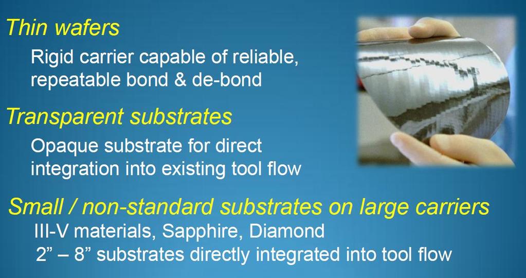
12 Material Handling Challenges Small Pieces Perforated wafers Flexible thin substrates Transparent substrates Small substrates e.g. InP Curved Surfaces
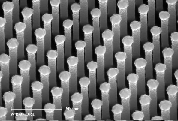
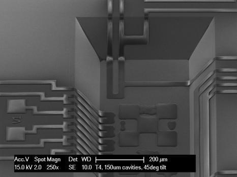
13 Processing Challenges Cantilevers T Gates Waveguides Nanotubes Lithography in 3D Photonic Crystals


14 Valley of Death Photonics Analog RF Bio Chips Power LEDs MEMS Solar Passives Collaborative Zone Collaborative Zone
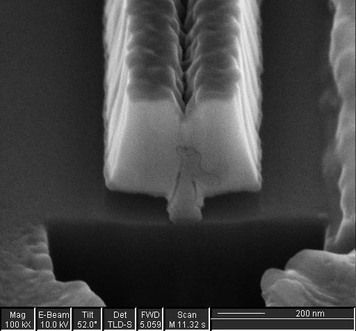
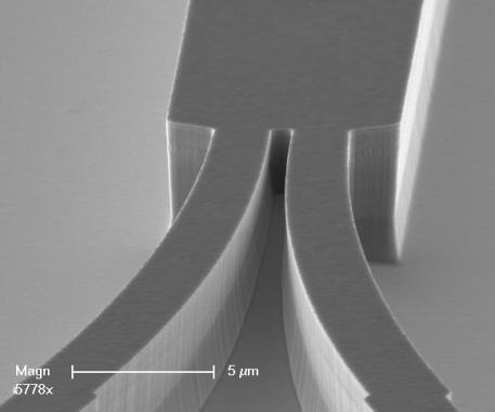
15 What are Specialty Foundries? Facilities that provide wafer processing services; from single steps, to complete product build, basically 3 types: Integrated device manufacturers (IDMs) who open up part of their fab for more than Moore activity Researchers who work within the University network R&D Small and Medium Enterprises (SME) utilize in house processes and ad hoc networks: Universities and other SMEs to produce new products e.g. Noel Technologies
16 What are Specialty Foundries? Provide customized processing services to researchers and industry: Significantly less material restrictions than CMOS facilities Thin and Thick substrates Transparent and perforated substrates Double side processing Substrate dimension requirements pieces to 300mm, later 450mm
17 Specialty Foundry Models Model Cost Time to Market IP Ownership Collaboration IDMs Low Intermediate Negotiated Yes University Labs Low Proof of concept Typically shared Research driven SMEs (Noel Technologies) Low Fast Your IP is your IP Yes Captive Foundry High Fast, restricted to mainstream Company Selective
18 University Labs California Universities have been increasing their capabilities R & D efforts are utilizing equipment built for manufacturing UCSB, UC Berkeley, UCLA, Stanford (SNF) have opened their doors to industry to provide access to researchers Industrial researchers can develop next technology node prototype devices prior to ramping up In some cases, Universities have more equipment capabilities than industry, however, collaboration is key to success


19 University Labs From Lab tools to Fab tools - UCSB ASML 5500/300 DUV Resolution 0.15um


20 University Labs From Lab tools to Fab tools - UCLA Headway Spinner - UCLA SVG 88 Series wafer track UCLA


21 University Labs From Lab tools to Fab tools - UCLA Automated CD SEM ASML 5500/200 i-line Resolution 0.35um

 with")
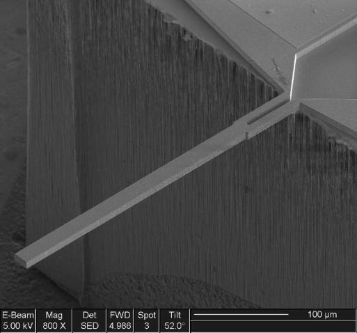
22 Enabling Technologies To address material handling challenges, Noel Technologies co-developed a unique Mobile Electrostatic Carrier (MESC) with Beam Services Inc.
23 Lithography Carriers

24 Existing Temporary Bonding Solutions


25 Existing Temporary Bonding Lithography Solutions Hot Plate removal Steam method 2 wafer mounted on 4 Silicon carrier with H20 droplets Dump rinse removal Method Capillary action


26 Enabling Technologies Beam Services MESC Low voltage, High Performance: 200+ hrs 400V charge Electrostatic force holds substrate in position on carrier
27 Design requirement - ASML Handling Must be able to cycle through system without hang ups Functionality - Must bond to target substrate firmly and cycle through system without sliding on carrier Flatness: <2um TTV Mechanical reproducibility: Substrate placement must be repeatable, within the capture range of the alignment system

28 Lithography Carriers
29 Testing Results 4 and 8 quartz mobile carriers were successfully used on ASML systems at Stanford University & SVTC Completed multiple cycles validating handling compliance with scanners and steppers 6 and 8 mobile carriers successfully used on ASML, Canon, Nikon and GCA systems
30 Conclusions A new era, beyond fruit, requires the same pioneering attitude as the Fairchild 8 go where no one has gone before Crossing the Valley of Death - Collaboration between SMEs and the University network provides a cost effective bridge from lab to fab New enabling technologies are providing pioneers with the tools they need to develop new products
31 Acknowledgements UC Berkeley, Marvell, Nanolab - UC Santa Barbara - Stanford Nanofab (SNF) - UC Los Angeles - Beam Services Inc. Steve Kent Noel Technologies


32 Specialty Foundry Noel Technologies, Inc. is a Silicon Valley based specialty foundry focused on process development, optimization, quality and delivery. An ISO 9001 registered facility, Noel Technologies offers process development and fabrication from 50mm up to 300mm
Application-Based Opportunities for Reused Fab Lines
 Application-Based Opportunities for Reused Fab Lines Semicon China, March 17 th 2010 Keith Best Simax Lithography S I M A X A L L I A N C E P A R T N E R S Outline Market: Exciting More than Moore applications
A Perspective on Semiconductor Equipment. R. B. Herring March 4, 2004
 A Perspective on Semiconductor Equipment R. B. Herring March 4, 2004 Outline Semiconductor Industry Overview of circuit fabrication Semiconductor Equipment Industry Some equipment business strategies Product
Photolithography I ( Part 1 )
") 1 Photolithography I ( Part 1 ) Chapter 13 : Semiconductor Manufacturing Technology by M. Quirk & J. Serda Bjørn-Ove Fimland, Department of Electronics and Telecommunication, Norwegian University of Science
1 Photolithography I ( Part 1 ) Chapter 13 : Semiconductor Manufacturing Technology by M. Quirk & J. Serda Bjørn-Ove Fimland, Department of Electronics and Telecommunication, Norwegian University of Science
Lithography in our Connected World
 Lithography in our Connected World SEMI Austin Spring Forum TOP PAN P R INTING CO., LTD MATER IAL SOLUTIONS DIVISION Toppan Printing Co., LTD A Broad-Based Global Printing Company Foundation: January 17,
Fabricating 2.5D, 3D, 5.5D Devices
 Fabricating 2.5D, 3D, 5.5D Devices Bob Patti, CTO rpatti@tezzaron.com Tezzar on Semiconduct or 04/15/2013 1 Gen4 Dis-Integrated 3D Memory DRAM layers 42nm node 2 million vertical connections per lay per
Progress due to: Feature size reduction - 0.7X/3 years (Moore s Law). Increasing chip size - 16% per year. Creativity in implementing functions.
. Increasing chip size - 16% per year. Creativity in implementing functions.") Introduction - Chapter 1 Evolution of IC Fabrication 1960 and 1990 integrated t circuits. it Progress due to: Feature size reduction - 0.7X/3 years (Moore s Law). Increasing chip size - 16% per year. Creativity
Introduction - Chapter 1 Evolution of IC Fabrication 1960 and 1990 integrated t circuits. it Progress due to: Feature size reduction - 0.7X/3 years (Moore s Law). Increasing chip size - 16% per year. Creativity
MAPPER: High throughput Maskless Lithography
 MAPPER: High throughput Maskless Lithography Marco Wieland CEA- Leti Alterative Lithography workshop 1 Today s agenda Introduction Applications Qualification of on-tool metrology by in-resist metrology
450mm and Moore s Law Advanced Packaging Challenges and the Impact of 3D
 450mm and Moore s Law Advanced Packaging Challenges and the Impact of 3D Doug Anberg VP, Technical Marketing Ultratech SOKUDO Lithography Breakfast Forum July 10, 2013 Agenda Next Generation Technology
MEMS in ECE at CMU. Gary K. Fedder
 MEMS in ECE at CMU Gary K. Fedder Department of Electrical and Computer Engineering and The Robotics Institute Carnegie Mellon University Pittsburgh, PA 15213-3890 fedder@ece.cmu.edu http://www.ece.cmu.edu/~mems
Waveguide-Integrated Optical Antenna nanoleds for On-Chip Communication
 Waveguide-Integrated Optical Antenna nanoleds for On-Chip Communication Michael Eggleston, Kevin Messer, Seth Fortuna, Eli Yablonovitch, Ming C. Wu Department of Electrical Engineering and Computer Sciences
University of California, Berkeley Department of Mechanical Engineering. ME 290R Topics in Manufacturing, Fall 2014: Lithography
 University of California, Berkeley Department of Mechanical Engineering ME 290R Topics in Manufacturing, Fall 2014: Lithography Class meetings: TuTh 3.30 5pm in 1165 Etcheverry Tentative class schedule
Feature-level Compensation & Control
 Feature-level Compensation & Control 2 Sensors and Control Nathan Cheung, Kameshwar Poolla, Costas Spanos Workshop 11/19/2003 3 Metrology, Control, and Integration Nathan Cheung, UCB SOI Wafers Multi wavelength
DOE Project: Resist Characterization
 DOE Project: Resist Characterization GOAL To achieve high resolution and adequate throughput, a photoresist must possess relatively high contrast and sensitivity to exposing radiation. The objective of
Holst Centre Wireless Autonomous Sensor Technologies & Flexible Electronics
 February 10, 2011 Holst Centre Wireless Autonomous Sensor Technologies & Flexible Electronics Presentation overview -General overview -Research focus < 4 Holst Centre: a solid partner in research Independent,
Market and technology trends in advanced packaging
 Close Market and technology trends in advanced packaging Executive OVERVIEW Recent advances in device miniaturization trends have placed stringent requirements for all aspects of product manufacturing.
2010 IRI Annual Meeting R&D in Transition
 2010 IRI Annual Meeting R&D in Transition U.S. Semiconductor R&D in Transition Dr. Peter J. Zdebel Senior VP and CTO ON Semiconductor May 4, 2010 Some Semiconductor Industry Facts Founded in the U.S. approximately
Nanotechnology, the infrastructure, and IBM s research projects
 Nanotechnology, the infrastructure, and IBM s research projects Dr. Paul Seidler Coordinator Nanotechnology Center, IBM Research - Zurich Nanotechnology is the understanding and control of matter at dimensions
Image sensor combining the best of different worlds
 Image sensors and vision systems Image sensor combining the best of different worlds First multispectral time-delay-and-integration (TDI) image sensor based on CCD-in-CMOS technology. Introduction Jonathan
MEMS for RF, Micro Optics and Scanning Probe Nanotechnology Applications
 MEMS for RF, Micro Optics and Scanning Probe Nanotechnology Applications Part I: RF Applications Introductions and Motivations What are RF MEMS? Example Devices RFIC RFIC consists of Active components
Silicon Photonics: A Platform for Integration, Wafer Level Assembly and Packaging
 Silicon Photonics: A Platform for Integration, Wafer Level Assembly and Packaging M. Asghari Kotura Inc April 27 Contents: Who is Kotura Choice of waveguide technology Challenges and merits of Si photonics
Nanostencil Lithography and Nanoelectronic Applications
 Microsystems Laboratory Nanostencil Lithography and Nanoelectronic Applications Oscar Vazquez, Marc van den Boogaart, Dr. Lianne Doeswijk, Prof. Juergen Brugger, LMIS1 Dr. Chan Woo Park, Visiting Professor
Flexible Hybrid Electronics Fabricated with High-Performance COTS ICs using RTI CircuitFilm TM Technology
 Flexible Hybrid Electronics Fabricated with High-Performance COTS ICs using RTI CircuitFilm TM Technology Scott Goodwin 1, Erik Vick 2 and Dorota Temple 2 1 Micross Advanced Interconnect Technology Micross
Beyond Moore the challenge for Europe
 Beyond Moore the challenge for Europe Dr. Alfred J. van Roosmalen Vice-President Business Development, NXP Semiconductors Company member of MEDEA+/CATRENE/AENEAS/Point-One FIT-IT 08 Spring Research Wien,
Mass transfer with elastomer stamps for microled displays.
 Frontiers in Assembly Mass transfer with elastomer stamps for microled displays. Matt Meitl X-Celeprint, Inc. mmeitl@x-celeprint.com 1 The best materials for the best displays The materials identify the
TXC Proprietary Info June 2012
 Purpose To introduce TXC s MO (MEMS Oscillator). Objectives What is a MO Different BOM Structure between MO and XO Product Feature Product Advantage Target Application Manufacturing Flow TXC Core Competence
Technology for the MEMS processing and testing environment. SUSS MicroTec AG Dr. Hans-Georg Kapitza
 Technology for the MEMS processing and testing environment SUSS MicroTec AG Dr. Hans-Georg Kapitza 1 SUSS MicroTec Industrial Group Founded 1949 as Karl Süss KG GmbH&Co. in Garching/ Munich San Jose Waterbury
Lecture: Integration of silicon photonics with electronics. Prepared by Jean-Marc FEDELI CEA-LETI
 Lecture: Integration of silicon photonics with electronics Prepared by Jean-Marc FEDELI CEA-LETI Context The goal is to give optical functionalities to electronics integrated circuit (EIC) The objectives
TSI, or through-silicon insulation, is the
 Vertical through-wafer insulation: Enabling integration and innovation PETER HIMES, Silex Microsystems AB, Järfälla SWEDEN Through-wafer insulation has been used to develop technologies such as Sil-Via
MEDIA RELEASE INSTITUTE OF MICROELECTRONICS KICKS OFF COPPER WIRE BONDING CONSORTIUM II TO TACKLE COPPER INTERCONNECTS RELIABILITY ISSUES
 MEDIA RELEASE INSTITUTE OF MICROELECTRONICS KICKS OFF COPPER WIRE BONDING CONSORTIUM II TO TACKLE COPPER INTERCONNECTS RELIABILITY ISSUES 1. Singapore, 25 March, 2013 -- The Institute of Microelectronics
450mm silicon wafers specification challenges. Mike Goldstein Intel Corp.
 450mm silicon wafers specification challenges Mike Goldstein Intel Corp. Outline Background 450mm transition program 450mm silicon evolution Mechanical grade wafers (spec case study) Developmental (test)
Introduction of ADVANTEST EB Lithography System
 Introduction of ADVANTEST EB Lithography System Nanotechnology Business Division ADVANTEST Corporation 1 2 Node [nm] EB Lithography Products < ADVANTEST s Superiority > High Resolution :EB optical technology
Mobile Electrostatic Carrier (MEC) evaluation for a GaAs wafer backside manufacturing process
 evaluation for a GaAs wafer backside manufacturing process") Mobile Electrostatic Carrier (MEC) evaluation for a GaAs wafer backside manufacturing process H.Stieglauer 1, J.Nösser 1, A.Miller 1, M.Lanz 1, D.Öttlin 1, G.Jonsson 1, D.Behammer 1, C.Landesberger 2,
Mobile Electrostatic Carrier (MEC) evaluation for a GaAs wafer backside manufacturing process H.Stieglauer 1, J.Nösser 1, A.Miller 1, M.Lanz 1, D.Öttlin 1, G.Jonsson 1, D.Behammer 1, C.Landesberger 2,
Intel's 65 nm Logic Technology Demonstrated on 0.57 µm 2 SRAM Cells
 Intel's 65 nm Logic Technology Demonstrated on 0.57 µm 2 SRAM Cells Mark Bohr Intel Senior Fellow Director of Process Architecture & Integration Intel 1 What are We Announcing? Intel has fabricated fully-functional
The SEMATECH Model: Potential Applications to PV
 Continually cited as the model for a successful industry/government consortium Accelerating the next technology revolution The SEMATECH Model: Potential Applications to PV Dr. Michael R. Polcari President
3D ICs: Recent Advances in the Industry
 3D ICs: Recent Advances in the Industry Suresh Ramalingam Senior Director, Advanced Packaging Outline 3D IC Background 3D IC Technology Development Summary Acknowledgements Stacked Silicon Interconnect
High-yield Fabrication Methods for MEMS Tilt Mirror Array for Optical Switches
 : MEMS Device Technologies High-yield Fabrication Methods for MEMS Tilt Mirror Array for Optical Switches Joji Yamaguchi, Tomomi Sakata, Nobuhiro Shimoyama, Hiromu Ishii, Fusao Shimokawa, and Tsuyoshi
Process Optimization
 Process Optimization Process Flow for non-critical layer optimization START Find the swing curve for the desired resist thickness. Determine the resist thickness (spin speed) from the swing curve and find
Chapter 1, Introduction
 Introduction to Semiconductor Manufacturing Technology Chapter 1, Introduction hxiao89@hotmail.com 1 Objective After taking this course, you will able to Use common semiconductor terminology Describe a
EE C245 ME C218 Introduction to MEMS Design
 EE C245 ME C218 Introduction to MEMS Design Fall 2008 Prof. Clark T.-C. Nguyen Dept. of Electrical Engineering & Computer Sciences University of California at Berkeley Berkeley, CA 94720 Lecture 1: Definition
EE105 Fall 2015 Microelectronic Devices and Circuits. Invention of Transistors
 EE105 Fall 2015 Microelectronic Devices and Circuits Prof. Ming C. Wu wu@eecs.berkeley.edu 511 Sutardja Dai Hall (SDH) 1-1 Invention of Transistors - 1947 Bardeen, Shockley, and Brattain at Bell Labs Invented
Des MEMS aux NEMS : évolution des technologies et des concepts aux travers des développements menés au LETI
 Des MEMS aux NEMS : évolution des technologies et des concepts aux travers des développements menés au LETI Ph. Robert 1 Content LETI at a glance From MEMS to NEMS: 30 years of technological evolution
InP-based Photonic Integration: Learning from CMOS
 InP-based Photonic Integration: Learning from CMOS Meint Smit Roel Baets Mike Wale COBRA TU Eindhoven IMEC U Gent Oclaro Receive Transmit Transponder-based DWDM FOE 2009, LS InP PIC in Dig Comm Networks,
Technology & Manufacturing
 Technology & Manufacturing Jean-Marc Chery Chief Operating Officer Front-End Manufacturing Unique capability 2 Technology portfolio aligned with application focus areas Flexible IDM model with foundry
EE C245 ME C218 Introduction to MEMS Design Fall 2010
 Instructor: Prof. Clark T.-C. Nguyen EE C245 ME C218 Introduction to MEMS Design Fall 2010 Prof. Clark T.-C. Nguyen Dept. of Electrical Engineering & Computer Sciences University of California at Berkeley
450mm patterning out of darkness Backend Process Exposure Tool SOKUDO Lithography Breakfast Forum July 10, 2013 Doug Shelton Canon USA Inc.
 450mm patterning out of darkness Backend Process Exposure Tool SOKUDO Lithography Breakfast Forum 2013 July 10, 2013 Doug Shelton Canon USA Inc. Introduction Half Pitch [nm] 2013 2014 2015 2016 2017 2018
SUNY Poly in a New Era
 SUNY Poly in a New Era Bahgat Sammakia Interim President, SUNY Polytechnic Institute SUNY Poly in a New Era Overview SUNY Poly is recognized as a global leader in advanced electronics Research and Development,
Manufacturing Development of a New Electroplated Magnetic Alloy Enabling Commercialization of PwrSoC Products
 Manufacturing Development of a New Electroplated Magnetic Alloy Enabling Commercialization of PwrSoC Products Trifon Liakopoulos, Amrit Panda, Matt Wilkowski and Ashraf Lotfi PowerSoC 2012 CONTENTS Definitions
Critical Dimension Enhancement of DUV Photolithography on the ASML 5500/300. Francesca Calderon Miramonte High School August 13th, 2015
 Critical Dimension Enhancement of DUV Photolithography on the ASML 5500/300 Francesca Calderon Miramonte High School August 13th, 2015 1 g-line - 436 nm i-line - 365 nm DUV - 248 nm DUV - 193 nm resolution
EUV Supporting Moore s Law
 EUV Supporting Moore s Law Marcel Kemp Director Investor Relations - Europe DB 2014 TMT Conference London September 4, 2014 Forward looking statements This document contains statements relating to certain
Flexline - A Flexible Manufacturing Method for Wafer Level Packages (Extended Abstract)
") Flexline - A Flexible Manufacturing Method for Wafer Level Packages (Extended Abstract) by Tom Strothmann, *Damien Pricolo, **Seung Wook Yoon, **Yaojian Lin STATS ChipPAC Inc.1711 W Greentree Drive Tempe,
Flexline - A Flexible Manufacturing Method for Wafer Level Packages (Extended Abstract) by Tom Strothmann, *Damien Pricolo, **Seung Wook Yoon, **Yaojian Lin STATS ChipPAC Inc.1711 W Greentree Drive Tempe,
DUV. Matthew McLaren Vice President Program Management, DUV. 24 November 2014
 DUV Matthew McLaren Vice President Program Management, DUV 24 Forward looking statements This document contains statements relating to certain projections and business trends that are forward-looking,
32nm High-K/Metal Gate Version Including 2nd Generation Intel Core processor family
 From Sand to Silicon Making of a Chip Illustrations 32nm High-K/Metal Gate Version Including 2nd Generation Intel Core processor family April 2011 1 The illustrations on the following foils are low resolution
Photonique sur silicium: Tendances et perspectives de marché
 From Technologies to Market Photonique sur silicium: Tendances et perspectives de marché Eric MOUNIER, YOLE DEVELOPPEMENT 2017 FIELDS OF EXPERTISE Yole Développement s 30 analysts operate in the following
Simulation of High Resistivity (CMOS) Pixels
 Pixels") Simulation of High Resistivity (CMOS) Pixels Stefan Lauxtermann, Kadri Vural Sensor Creations Inc. AIDA-2020 CMOS Simulation Workshop May 13 th 2016 OUTLINE 1. Definition of High Resistivity Pixel Also
Simulation of High Resistivity (CMOS) Pixels Stefan Lauxtermann, Kadri Vural Sensor Creations Inc. AIDA-2020 CMOS Simulation Workshop May 13 th 2016 OUTLINE 1. Definition of High Resistivity Pixel Also
Index. Cambridge University Press Silicon Photonics Design Lukas Chrostowski and Michael Hochberg. Index.
 absorption, 69 active tuning, 234 alignment, 394 396 apodization, 164 applications, 7 automated optical probe station, 389 397 avalanche detector, 268 back reflection, 164 band structures, 30 bandwidth
Part 5-1: Lithography
 Part 5-1: Lithography Yao-Joe Yang 1 Pattern Transfer (Patterning) Types of lithography systems: Optical X-ray electron beam writer (non-traditional, no masks) Two-dimensional pattern transfer: limited
The Department of Advanced Materials Engineering. Materials and Processes in Polymeric Microelectronics
 The Department of Advanced Materials Engineering Materials and Processes in Polymeric Microelectronics 1 Outline Materials and Processes in Polymeric Microelectronics Polymeric Microelectronics Process
Evaluating and Optimizing Tradeoffs in CMOS RFIC Upconversion Mixer Design. by Dr. Stephen Long University of California, Santa Barbara
 Evaluating and Optimizing Tradeoffs in CMOS RFIC Upconversion Mixer Design by Dr. Stephen Long University of California, Santa Barbara It is not easy to design an RFIC mixer. Different, sometimes conflicting,
IMAPS NE 45 A HETEROGENEOUS SIP SOLUTION FOR RF APPLICATIONS
 IMAPS NE 45 A HETEROGENEOUS SIP SOLUTION FOR RF APPLICATIONS May 1st 2018 Justin C. Borski i3 Microsystems Inc. justin.borski@i3microsystems.com A HETEROGENEOUS SIP SOLUTION FOR RF APPLICATIONS Presentation
Plan Optik AG. Plan Optik AG PRODUCT CATALOGUE
 Plan Optik AG Plan Optik AG PRODUCT CATALOGUE 2 In order to service the high demand of wafers more quickly, Plan Optik provides off the shelf products in sizes from 2 up to 300mm diameter. Therefore Plan
Recent Innovations in MEMS Sensors for PNT Applications
 Recent Innovations in MEMS Sensors for PNT Applications Stanford PNT Symposium 2017 Alissa M. Fitzgerald, Ph.D. Founder & CEO amf@amfitzgerald.com Overview Navigation Developments in MEMS gyroscope technology
DTU DANCHIP an open access micro/nanofabrication facility bridging academic research and small scale production
 DTU DANCHIP an open access micro/nanofabrication facility bridging academic research and small scale production DTU Danchip National Center for Micro- and Nanofabrication DTU Danchip DTU Danchip is Denmark
IMPACT OF 450MM ON CMP
 IMPACT OF 450MM ON CMP MICHAEL CORBETT MANAGING PARTNER LINX CONSULTING, LLC MCORBETT@LINX-CONSULTING.COM PREPARED FOR CMPUG JULY 2011 LINX CONSULTING Outline 1. Overview of Linx Consulting 2. CMP Outlook/Drivers
Innovative Mask Aligner Lithography for MEMS and Packaging
 Innovative Mask Aligner Lithography for MEMS and Packaging Dr. Reinhard Voelkel CEO SUSS MicroOptics SA September 9 th, 2010 1 SUSS Micro-Optics SUSS MicroOptics is a leading supplier for high-quality
Applications of Maskless Lithography for the Production of Large Area Substrates Using the SF-100 ELITE. Jay Sasserath, PhD
 Applications of Maskless Lithography for the Production of Large Area Substrates Using the SF-100 ELITE Executive Summary Jay Sasserath, PhD Intelligent Micro Patterning LLC St. Petersburg, Florida Processing
My USM. Mustafa G. Guvench. Professor, Electrical Engineering
 My Projects @ USM Mustafa G. Guvench Professor, Electrical Engineering My Interests & Expertise CMOS Analog I.C. Design Silicon I.C. Processing Micro Machining and MEMS Optoelectronics (Photosensors( Photosensors)
Strategies for low cost imprint molds
 Strategies for low cost imprint molds M.P.C. Watts, Impattern Solutions, 9404 Bell Mountain Drive Austin TX 78730 www.impattern.com ABSTRACT The Cost of ownership (COO) due to the mold can be minimized
HOW TO CONTINUE COST SCALING. Hans Lebon
 HOW TO CONTINUE COST SCALING Hans Lebon OUTLINE Scaling & Scaling Challenges Imec Technology Roadmap Wafer size scaling : 450 mm 2 COST SCALING IMPROVED PERFORMANCE 3 GLOBAL TRAFFIC FORECAST Cloud Traffic
Recent Developments in Multifunctional Integration. Stephan Guttowski, Head of Technology Park»Heterointegration«, Fraunhofer FMD
 Recent Developments in Multifunctional Integration Stephan Guttowski, Head of Technology Park»Heterointegration«, Fraunhofer FMD Founding Participants 2 One-Stop-Shop for developments from wafer technologies
45nm Foundry CMOS with Mask-Lite Reduced Mask Costs
 This work is sponsored in part by the Air Force Research Laboratory (AFRL/RVSE) 45nm Foundry CMOS with Mask-Lite Reduced Mask Costs 21 March 2012 This work is sponsored in part by the National Aeronautics
Laser patterning and projection lithography
 Introduction to Nanofabrication Techniques: Laser patterning and projection lithography Benjamin Johnston Macquarie University David O Connor Bandwidth Foundry - USYD The OptoFab node of ANFF Broad ranging
SWTW 2000, June Assessing Pad Damage and Bond Integrity for Fine Pitch Probing
 SWTW 2000, June 11-14 Assessing Pad Damage and Bond Integrity for Fine Pitch Probing Dean Gahagan, Pyramid Probe Division, Cascade Microtech & Lee Levine, Kulicke & Soffa Industries Challenges of die shrinks
IMPACT Roundtable Lithography + DfM
 IMPACT Roundtable Lithography + DfM Andy Neureuther Electrical Engineering & Computer Science September 24, 2008 neureuth@eecsberkeley.edu 510.642.4590 University of California Berkeley San Diego Los Angeles
Sonion TC100Z21A DigiSiMic Silicon Condensor Microphone MEMS Process Review
 November 8, 2006 Sonion TC100Z21A DigiSiMic Silicon Condensor Microphone MEMS Process Review For comments, questions, or more information about this report, or for any additional technical needs concerning
TWINSCAN XT:1950i Water-based immersion taken to the max Enabling fast, single-exposure lithography at sub 40 nm
 TWINSCAN XT:1950i Water-based immersion taken to the max Enabling fast, single-exposure lithography at sub 40 nm SEMICON West, San Francisco July 14-18, 2008 Slide 1 The immersion pool becomes an ocean
Introduction to VLSI ASIC Design and Technology
 Introduction to VLSI ASIC Design and Technology Paulo Moreira CERN - Geneva, Switzerland Paulo Moreira Introduction 1 Outline Introduction Is there a limit? Transistors CMOS building blocks Parasitics
Reducing MEMS product development and commercialization time
 Reducing MEMS product development and commercialization time Introduction Fariborz Maseeh, Andrew Swiecki, Nora Finch IntelliSense Corporation 36 Jonspin Road, Wilmington MA 01887 www.intellisense.com
Winter College on Optics: Fundamentals of Photonics - Theory, Devices and Applications February 2014
 2572-10 Winter College on Optics: Fundamentals of Photonics - Theory, Devices and Applications 10-21 February 2014 Photonic packaging and integration technologies II Sonia M. García Blanco University of
IWORID J. Schmitz page 1. Wafer-level CMOS post-processing Jurriaan Schmitz
 IWORID J. Schmitz page 1 Wafer-level CMOS post-processing Jurriaan Schmitz IWORID J. Schmitz page 2 Outline Introduction on wafer-level post-proc. CMOS: a smart, but fragile substrate Post-processing steps
Projects and Partners Working with Chalcogenide Advanced Manufacturing Partnership (ChAMP)
") Projects and Partners Working with Chalcogenide Advanced Manufacturing Partnership (ChAMP) Dr John Lincoln Industrial Liaison Officer j.lincoln@soton.ac.uk March 2015 ChAMP Aims Establish world leading
Projects and Partners Working with Chalcogenide Advanced Manufacturing Partnership (ChAMP) Dr John Lincoln Industrial Liaison Officer j.lincoln@soton.ac.uk March 2015 ChAMP Aims Establish world leading
Update: SOI Wafer Market Continues Its Growth
 Gartner Dataquest Alert Update: SOI Wafer Market Continues Its Growth The results of Gartner Dataquest's latest survey of the silicon on insulator (SOI) wafer market indicate demand grew 16 percent in
45nm Foundry CMOS with Mask-Lite Reduced Mask Costs
 This work is sponsored by the Air Force Research Laboratory (AFRL/RVSE) TPOC: Mr. Kenneth Hebert 45nm Foundry CMOS with Mask-Lite Reduced Mask Costs 25 October 2011 www.americansemi.com 2011 American Semiconductor,
DTU DANCHIP an open access micro/nanofabrication facility bridging academic research and small scale production
 DTU DANCHIP an open access micro/nanofabrication facility bridging academic research and small scale production DTU Danchip National Center for Micro- and Nanofabrication DTU Danchip DTU Danchip is Denmark
Emerging MEMS & Sensor Technologies to Watch: Alissa M. Fitzgerald, Ph.D., Founder & CEO Semicon West 2018
 Emerging MEMS & Sensor Technologies to Watch: 2018 Alissa M. Fitzgerald, Ph.D., Founder & CEO amf@amfitzgerald.com Outline About AMFitzgerald What emerging means in this presentation Emerging MEMS & sensor
Outline. 1 Introduction. 2 Basic IC fabrication processes. 3 Fabrication techniques for MEMS. 4 Applications. 5 Mechanics issues on MEMS MDL NTHU
 Outline 1 Introduction 2 Basic IC fabrication processes 3 Fabrication techniques for MEMS 4 Applications 5 Mechanics issues on MEMS 2.2 Lithography Reading: Runyan Chap. 5, or 莊達人 Chap. 7, or Wolf and
(12) Patent Application Publication (10) Pub. No.: US 2003/ A1
 Patent Application Publication (10) Pub. No.: US 2003/ A1") US 20030091084A1 (19) United States (12) Patent Application Publication (10) Pub. No.: US 2003/0091084A1 Sun et al. (43) Pub. Date: May 15, 2003 (54) INTEGRATION OF VCSEL ARRAY AND Publication Classification
US 20030091084A1 (19) United States (12) Patent Application Publication (10) Pub. No.: US 2003/0091084A1 Sun et al. (43) Pub. Date: May 15, 2003 (54) INTEGRATION OF VCSEL ARRAY AND Publication Classification
Optical Microlithography XXVIII
 PROCEEDINGS OF SPIE Optical Microlithography XXVIII Kafai Lai Andreas Erdmann Editors 24-26 February 2015 San Jose, California, United States Sponsored by SPIE Cosponsored by Cymer, an ASML company (United
DC-40GHz ATTENUATOR. GaAs Monolithic Microwave IC. Insertion Loss ( db )
") Insertion Loss ( ) Description The is a variable DC-40GHz attenuator designed for a wide range of applications, from military to commercial communication systems. The chip backside is both RF and DC grounds.
Insertion Loss ( ) Description The is a variable DC-40GHz attenuator designed for a wide range of applications, from military to commercial communication systems. The chip backside is both RF and DC grounds.
Doug Dunn ASML President and Chief Executive Officer Deutsche Bank Conference London, England September 19, / Slide 1
 Doug Dunn ASML President and Chief Executive Officer Deutsche Bank Conference London, England September 19, 2003 / Slide 1 Safe Harbor Safe Harbor Statement under the U.S. Private Securities Litigation
(Complementary E-Beam Lithography)
") Extending Optical Lithography with C E B L (Complementary E-Beam Lithography) July 13, 2011 4008 Burton Drive, Santa Clara, CA 95054 Outline Complementary Lithography E-Beam Complements Optical Multibeam
Extending Optical Lithography with C E B L (Complementary E-Beam Lithography) July 13, 2011 4008 Burton Drive, Santa Clara, CA 95054 Outline Complementary Lithography E-Beam Complements Optical Multibeam
POSSUM TM Die Design as a Low Cost 3D Packaging Alternative
 POSSUM TM Die Design as a Low Cost 3D Packaging Alternative The trend toward 3D system integration in a small form factor has accelerated even more with the introduction of smartphones and tablets. Integration
Optical Lithography. Keeho Kim Nano Team / R&D DongbuAnam Semi
 Optical Lithography Keeho Kim Nano Team / R&D DongbuAnam Semi Contents Lithography = Photolithography = Optical Lithography CD : Critical Dimension Resist Pattern after Development Exposure Contents Optical
Body-Biased Complementary Logic Implemented Using AlN Piezoelectric MEMS Switches
 University of Pennsylvania From the SelectedWorks of Nipun Sinha 29 Body-Biased Complementary Logic Implemented Using AlN Piezoelectric MEMS Switches Nipun Sinha, University of Pennsylvania Timothy S.
Extending The Life Of 200mm Fabs And The Re-use of Second Hand Tools
 Extending The Life Of 200mm Fabs And The Re-use of Second Hand Tools Gareth Bignell, FE Equipment Procurement Director SEMICON Europa 2012 Presentation Summary 2 An introduction to STMicroelectronics The
Advanced Packaging Lithography and Inspection Solutions for Next Generation FOWLP-FOPLP Processing
 Advanced Packaging Lithography and Inspection Solutions for Next Generation FOWLP-FOPLP Processing Keith Best, Gurvinder Singh, and Roger McCleary Rudolph Technologies, Inc. 16 Jonspin Rd. Wilmington,
Through-Silicon-Via Inductor: Is it Real or Just A Fantasy?
 Through-Silicon-Via Inductor: Is it Real or Just A Fantasy? Umamaheswara Rao Tida 1 Cheng Zhuo 2 Yiyu Shi 1 1 ECE Department, Missouri University of Science and Technology 2 Intel Research, Hillsboro Outline
Packaging Roadmap: The impact of miniaturization. Bob Pfahl, inemi Celestica-iNEMI Technology Forum May 15, 2007
 Packaging Roadmap: The impact of miniaturization Bob Pfahl, inemi Celestica-iNEMI Technology Forum May 15, 2007 The Challenges for the Next Decade Addressing the consumer experience using the converged
Lecture 1 Introduction to Solid State Electronics
 EE 471: Transport Phenomena in Solid State Devices Spring 2018 Lecture 1 Introduction to Solid State Electronics Bryan Ackland Department of Electrical and Computer Engineering Stevens Institute of Technology
SAMPLE SLIDES & COURSE OUTLINE. Core Competency In Semiconductor Technology: 2. FABRICATION. Dr. Theodore (Ted) Dellin
 Dellin") & Digging Deeper Devices, Fabrication & Reliability For More Info:.com or email Dellin@ieee.org SAMPLE SLIDES & COURSE OUTLINE In : 2. A Easy, Effective, of How Devices Are.. Recommended for everyone who
& Digging Deeper Devices, Fabrication & Reliability For More Info:.com or email Dellin@ieee.org SAMPLE SLIDES & COURSE OUTLINE In : 2. A Easy, Effective, of How Devices Are.. Recommended for everyone who
ATV 2011: Computer Engineering
 ATV 2011: Technology Trends in Computer Engineering Professor Per Larsson-Edefors ATV 2011, L1, Per Larsson-Edefors Page 1 Solid-State Devices www.cse.chalmers.se/~perla/ugrad/ SemTech/Lectures_2000.pdf