IWORID J. Schmitz page 1. Wafer-level CMOS post-processing Jurriaan Schmitz
|
|
|
- Winifred Ryan
- 5 years ago
- Views:
Transcription

1 IWORID J. Schmitz page 1 Wafer-level CMOS post-processing Jurriaan Schmitz
2 IWORID J. Schmitz page 2 Outline Introduction on wafer-level post-proc. CMOS: a smart, but fragile substrate Post-processing steps System examples Conclusions

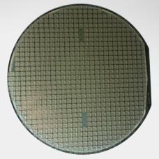
3 IWORID J. Schmitz page 3 45 years of integrated circuits Enormous skill in micro-manufacturing High performance computing Solid-state memories Can we do more with this skill than number crunching and memorizing? One approach: wafer level post-processing

4 IWORID J. Schmitz page 4 Wafer-level post-processing Add process steps only here


5 There s plenty of room at the top IWORID J. Schmitz page 5
6 IWORID J. Schmitz page 6 The idea of CMOS post-proc. (1) Wafer-scale post-processing: Chips are finished and fully functional No intrusion into clean IC fab Still benefit from planar technology (yield, efficiency, cost, existing toolkit ) A microchip is fragile, so take care!
 Attractive when: The monolithic solution is cheaper (saving assembly & testing expenses) The monolithic solution")
7 IWORID J. Schmitz page 7 The idea of CMOS post-proc. (2) Attractive when: The monolithic solution is cheaper (saving assembly & testing expenses) The monolithic solution outperforms hybrid technologies Size matters See
8 IWORID J. Schmitz page 8 Is post-processing trivial? 1. The chip is vulnerable: Heat > 400 ºC destroys the metallization Plasma charging destroys the MOSFETs Mechanical stress changes components H 2 passivation must be maintained 2. Packaging has to be re-invented. Without package: contamination 3. How to deposit high-quality thin films?
9 IWORID J. Schmitz page 9 High temperature in IC fabrication Heat is necessary during IC fabrication: To oxidise silicon To diffuse impurities in silicon To repair silicon lattice damage To activate impurities To deposit materials by CVD To initiate reactions, e.g. Ti+2Si TiSi 2
10 IWORID J. Schmitz page 10 Deposition Oxidation Anneal Pad oxide Si3 N 4 HDP trench fill STI sidewall Si3 N 4 sacox Well anneal Gate oxide Gate RTA (predoping) Poly reoxidation Extension RTAs Si3 N 4 spacer Gate/s/d RTA Si3 N 4 deopsition Locsal RTA 2nd silicide RTA time Temperature ( C)
11 IWORID J. Schmitz page 11 Thermal budget of an IC Keep it cool(er) Transistor ready: stop diffusion wires ready: avoid Al melt Soldering ready: avoid solder melt Temperature (ºC) Front-end 1000 Back-end 500 Packaging 300 Soldering 200 Time

12 IWORID J. Schmitz page 12 Thermal budget trend Smaller dimension transistors: diffusion should be reduced High-temperature steps are reduced in time and temperature, where possible New machines (RTP, laser) New materials (SiLK) New techniques (ICP-CVD)
13 IWORID J. Schmitz page 13 (Post) process-induced damage Mechanical damage (e.g. scratches) Electrostatic discharges Plasma damage in IC technology: Plasma etching Plasma-assisted depositions (PECVD) Photoresist removal All three: hard to do without!


14 IWORID J. Schmitz page 14 Plasma etching Ions bombarding the surface Radicals reacting with atoms


15 IWORID J. Schmitz page 15 Plasma etching induced damage High anisotropy vertical profiles Charge pile-up can lead to discharging inside the chip plasma SiO 2 Wafer MOS gate
16 The antenna effect IWORID J. Schmitz page 16
17 IWORID J. Schmitz page 17 Plasma processing induced damage Suppression: Adopt design rules (unfit for wafer-scale post-processing) Tune the plasma settings Use other approach (e.g. remove photoresist in a liquid)
 Hot processing leads to H 2 outgassing")
18 IWORID J. Schmitz page 18 Other alerts H 2 passivation essential for MOSFET Final alloy step ( ºC in H 2 /N 2 ) Hot processing leads to H 2 outgassing Mechanical stress should stay low Metal ions can ruin the chip, even at room temperature! Stick to IC mfg. rules Eijkelboom et al., ECN 2002
 IWORID J.")
19 May we introduce a new material? (source: IWORID J. Schmitz page 19

20 IWORID J. Schmitz page 20 What is allowed above CMOS? All backend tricks can be repeated! Metal deposition Dielectric deposition CMP Patterning Semiconductors? Polymers? Suspended structures?

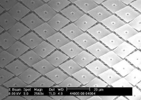
21 IWORID J. Schmitz page 21 Example: Medipix2 modification Technique: wafer-level lift-off lithography, using aluminum Result: Medipix2 still fully functional Good for ball-grid-arrays Good for gaseous particle detection
22 IWORID J. Schmitz page 22 CMOS post-proc. steps (3) Chemical Mechanical Polishing allows to pattern any new material E.g. piezo-electric films, ferro-electrics


23 IWORID J. Schmitz page 23 Dielectric and semiconductor thin films Some activation energy is necessary to form strong bonds Low-temp depositions: ECR-CVD, ICP-CVD Laser crystallization?
 BCB Parylene Structural material: rigidity residual stress impact on IC")
24 IWORID J. Schmitz page 24 Suspended structures Sacrificial material: SU8 SiGe (T. J. King et al., UCB) BCB Parylene Structural material: rigidity residual stress impact on IC
25 IWORID J. Schmitz page 25 wlpp microsystems CMOS image sensor LCOS Micromirrors Ultrasound imaging detectors SIAM X-ray detectors Integrated Micromegas Integrated microchannel plate


26 IWORID J. Schmitz page 26 The CMOS image sensor (= monolithic active pixel sensor) Incident light lens R/G/B filter lens R/G/B filter Standard CMOS photodiode silicon photodiode
 Transparent")
27 IWORID J. Schmitz page 27 Liquid crystal on silicon (LCOS) Transparent electrode Liquid crystal Mirror electrode Standard CMOS silicon
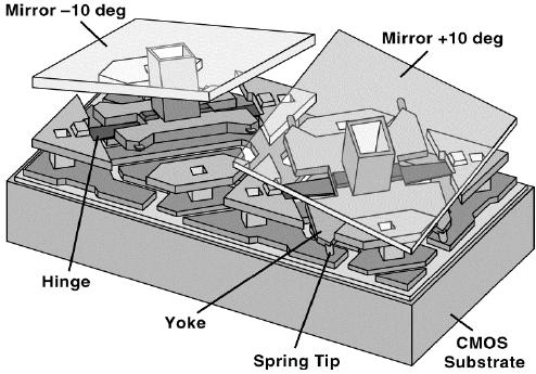
28 TI s micromirrors IWORID J. Schmitz page 28

29 IWORID J. Schmitz page 29


30 IWORID J. Schmitz page 30 Ultrasound detector arrays Sensant (now acquired by Siemens)

31 IWORID J. Schmitz page 31 Monolithic X-ray detector SIAM collaboration

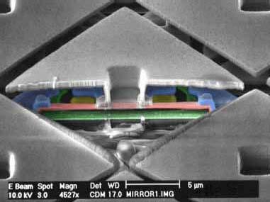
32 IWORID J. Schmitz page 32 The GOSSIP gaseous detector HV cathode V. Carballo Blanco et al., IWORID 2006 Naked Medipix2 chip
33 IWORID J. Schmitz page 33 Integrated microchannel plates Principle: J. Vallerga et al., IWORID 2004 Wafer-level manufacturing: Porous alumina? Naked Medipix2 chip J. Melai et al., IWORID 2006
34 IWORID J. Schmitz page 34 Conclusions IC Technology now offers a wide range of manufacturing techniques Computing and data storage + extra s Many new microsystems under study Our focus: systems with high internal data rates wiring is not an option
35 IWORID J. Schmitz page 35 Acknowledgements Thanks to: The IWORID committee Dutch Technology Foundation STW Our academic and industrial partners My coworkers
CMP for More Than Moore
 2009 Levitronix Conference on CMP Gerfried Zwicker Fraunhofer Institute for Silicon Technology ISIT Itzehoe, Germany gerfried.zwicker@isit.fraunhofer.de Contents Moore s Law and More Than Moore Comparison:
CMOS Digital Integrated Circuits Lec 2 Fabrication of MOSFETs
 CMOS Digital Integrated Circuits Lec 2 Fabrication of MOSFETs 1 CMOS Digital Integrated Circuits 3 rd Edition Categories of Materials Materials can be categorized into three main groups regarding their
2.8 - CMOS TECHNOLOGY
 CMOS Technology (6/7/00) Page 1 2.8 - CMOS TECHNOLOGY INTRODUCTION Objective The objective of this presentation is: 1.) Illustrate the fabrication sequence for a typical MOS transistor 2.) Show the physical
420 Intro to VLSI Design
 Dept of Electrical and Computer Engineering 420 Intro to VLSI Design Lecture 0: Course Introduction and Overview Valencia M. Joyner Spring 2005 Getting Started Syllabus About the Instructor Labs, Problem
Chapter 15 Summary and Future Trends
 Chapter 15 Summary and Future Trends Hong Xiao, Ph. D. hxiao89@hotmail.com www2.austin.cc.tx.us/hongxiao/book.htm Hong Xiao, Ph. D. www2.austin.cc.tx.us/hongxiao/book.htm 1 The 1960s First IC product Bipolar
Integrated diodes. The forward voltage drop only slightly depends on the forward current. ELEKTRONIKOS ĮTAISAI
 1 Integrated diodes pn junctions of transistor structures can be used as integrated diodes. The choice of the junction is limited by the considerations of switching speed and breakdown voltage. The forward
Chapter 3: Basics Semiconductor Devices and Processing 2006/9/27 1. Topics
 Chapter 3: Basics Semiconductor Devices and Processing 2006/9/27 1 Topics What is semiconductor Basic semiconductor devices Basics of IC processing CMOS technologies 2006/9/27 2 1 What is Semiconductor
Lecture: Integration of silicon photonics with electronics. Prepared by Jean-Marc FEDELI CEA-LETI
 Lecture: Integration of silicon photonics with electronics Prepared by Jean-Marc FEDELI CEA-LETI Context The goal is to give optical functionalities to electronics integrated circuit (EIC) The objectives
Chapter 3 Basics Semiconductor Devices and Processing
 Chapter 3 Basics Semiconductor Devices and Processing 1 Objectives Identify at least two semiconductor materials from the periodic table of elements List n-type and p-type dopants Describe a diode and
SAMPLE SLIDES & COURSE OUTLINE. Core Competency In Semiconductor Technology: 2. FABRICATION. Dr. Theodore (Ted) Dellin
 Dellin") & Digging Deeper Devices, Fabrication & Reliability For More Info:.com or email Dellin@ieee.org SAMPLE SLIDES & COURSE OUTLINE In : 2. A Easy, Effective, of How Devices Are.. Recommended for everyone who
& Digging Deeper Devices, Fabrication & Reliability For More Info:.com or email Dellin@ieee.org SAMPLE SLIDES & COURSE OUTLINE In : 2. A Easy, Effective, of How Devices Are.. Recommended for everyone who
Transistor was first invented by William.B.Shockley, Walter Brattain and John Bardeen of Bell Labratories. In 1961, first IC was introduced.
 Unit 1 Basic MOS Technology Transistor was first invented by William.B.Shockley, Walter Brattain and John Bardeen of Bell Labratories. In 1961, first IC was introduced. Levels of Integration:- i) SSI:-
VLSI Design. Introduction
 Tassadaq Hussain VLSI Design Introduction Outcome of this course Problem Aims Objectives Outcomes Data Collection Theoretical Model Mathematical Model Validate Development Analysis and Observation Pseudo
FABRICATION OF CMOS INTEGRATED CIRCUITS. Dr. Mohammed M. Farag
 FABRICATION OF CMOS INTEGRATED CIRCUITS Dr. Mohammed M. Farag Outline Overview of CMOS Fabrication Processes The CMOS Fabrication Process Flow Design Rules Reference: Uyemura, John P. "Introduction to
State-of-the-art device fabrication techniques
 State-of-the-art device fabrication techniques! Standard Photo-lithography and e-beam lithography! Advanced lithography techniques used in semiconductor industry Deposition: Thermal evaporation, e-gun
Lecture 020 ECE4430 Review II (1/5/04) Page 020-1
 Page 020-1") Lecture 020 ECE4430 Review II (1/5/04) Page 020-1 LECTURE 020 ECE 4430 REVIEW II (READING: GHLM - Chap. 2) Objective The objective of this presentation is: 1.) Identify the prerequisite material as taught
Lecture 020 ECE4430 Review II (1/5/04) Page 020-1 LECTURE 020 ECE 4430 REVIEW II (READING: GHLM - Chap. 2) Objective The objective of this presentation is: 1.) Identify the prerequisite material as taught
Photolithography I ( Part 1 )
") 1 Photolithography I ( Part 1 ) Chapter 13 : Semiconductor Manufacturing Technology by M. Quirk & J. Serda Bjørn-Ove Fimland, Department of Electronics and Telecommunication, Norwegian University of Science
1 Photolithography I ( Part 1 ) Chapter 13 : Semiconductor Manufacturing Technology by M. Quirk & J. Serda Bjørn-Ove Fimland, Department of Electronics and Telecommunication, Norwegian University of Science
Session 3: Solid State Devices. Silicon on Insulator
 Session 3: Solid State Devices Silicon on Insulator 1 Outline A B C D E F G H I J 2 Outline Ref: Taurand Ning 3 SOI Technology SOl materials: SIMOX, BESOl, and Smart Cut SIMOX : Synthesis by IMplanted
Hermetic Packaging Solutions using Borosilicate Glass Thin Films. Lithoglas Hermetic Packaging Solutions using Borosilicate Glass Thin Films
 Hermetic Packaging Solutions using Borosilicate Glass Thin Films 1 Company Profile Company founded in 2006 ISO 9001:2008 qualified since 2011 Headquarters and Production in Dresden, Germany Production
EE4800 CMOS Digital IC Design & Analysis. Lecture 1 Introduction Zhuo Feng
 EE4800 CMOS Digital IC Design & Analysis Lecture 1 Introduction Zhuo Feng 1.1 Prof. Zhuo Feng Office: EERC 730 Phone: 487-3116 Email: zhuofeng@mtu.edu Class Website http://www.ece.mtu.edu/~zhuofeng/ee4800fall2010.html
Simulation of High Resistivity (CMOS) Pixels
 Pixels") Simulation of High Resistivity (CMOS) Pixels Stefan Lauxtermann, Kadri Vural Sensor Creations Inc. AIDA-2020 CMOS Simulation Workshop May 13 th 2016 OUTLINE 1. Definition of High Resistivity Pixel Also
Simulation of High Resistivity (CMOS) Pixels Stefan Lauxtermann, Kadri Vural Sensor Creations Inc. AIDA-2020 CMOS Simulation Workshop May 13 th 2016 OUTLINE 1. Definition of High Resistivity Pixel Also
Nanotechnology, the infrastructure, and IBM s research projects
 Nanotechnology, the infrastructure, and IBM s research projects Dr. Paul Seidler Coordinator Nanotechnology Center, IBM Research - Zurich Nanotechnology is the understanding and control of matter at dimensions
MEMS in ECE at CMU. Gary K. Fedder
 MEMS in ECE at CMU Gary K. Fedder Department of Electrical and Computer Engineering and The Robotics Institute Carnegie Mellon University Pittsburgh, PA 15213-3890 fedder@ece.cmu.edu http://www.ece.cmu.edu/~mems
EE C245 ME C218 Introduction to MEMS Design
 EE C45 ME C18 Introduction to MEMS Design Fall 008 Prof. Clark T.-C. Nguyen Dept. of Electrical Engineering & Computer Sciences University of California at Berkeley Berkeley, CA 9470 Lecture 7: Noise &
Fabricating 2.5D, 3D, 5.5D Devices
 Fabricating 2.5D, 3D, 5.5D Devices Bob Patti, CTO rpatti@tezzaron.com Tezzar on Semiconduct or 04/15/2013 1 Gen4 Dis-Integrated 3D Memory DRAM layers 42nm node 2 million vertical connections per lay per
Powerchip Semiconductor Corporation A3R12E3GEF G6E 635BLC4M 512 Megabit DDR2 SDRAM Structural Analysis
 February 23, 2007 Powerchip Semiconductor Corporation A3R12E3GEF G6E 635BLC4M Structural Analysis For comments, questions, or more information about this report, or for any additional technical needs concerning
Lecture 0: Introduction
 Lecture 0: Introduction Introduction Integrated circuits: many transistors on one chip. Very Large Scale Integration (VLSI): bucketloads! Complementary Metal Oxide Semiconductor Fast, cheap, low power
VLSI Design. Introduction
 VLSI Design Introduction Outline Introduction Silicon, pn-junctions and transistors A Brief History Operation of MOS Transistors CMOS circuits Fabrication steps for CMOS circuits Introduction Integrated
3D SOI elements for System-on-Chip applications
 Advanced Materials Research Online: 2011-07-04 ISSN: 1662-8985, Vol. 276, pp 137-144 doi:10.4028/www.scientific.net/amr.276.137 2011 Trans Tech Publications, Switzerland 3D SOI elements for System-on-Chip
Wireless Metrology in Semiconductor Manufacturing
 1 Wireless Metrology in Semiconductor Manufacturing Costas J. Spanos Seminar 2 Outline Historical perspective Hardware and software applications Breakthroughs that have yet to be realized Distributed control
Si and InP Integration in the HELIOS project
 Si and InP Integration in the HELIOS project J.M. Fedeli CEA-LETI, Grenoble ( France) ECOC 2009 1 Basic information about HELIOS HELIOS photonics ELectronics functional Integration on CMOS www.helios-project.eu
A Low-cost Through Via Interconnection for ISM WLP
 A Low-cost Through Via Interconnection for ISM WLP Jingli Yuan, Won-Kyu Jeung, Chang-Hyun Lim, Seung-Wook Park, Young-Do Kweon, Sung Yi To cite this version: Jingli Yuan, Won-Kyu Jeung, Chang-Hyun Lim,
Basic Fabrication Steps
 Basic Fabrication Steps and Layout Somayyeh Koohi Department of Computer Engineering Adapted with modifications from lecture notes prepared by author Outline Fabrication steps Transistor structures Transistor
Aptina MT9P111 5 Megapixel, 1/4 Inch Optical Format, System-on-Chip (SoC) CMOS Image Sensor
 CMOS Image Sensor") Aptina MT9P111 5 Megapixel, 1/4 Inch Optical Format, System-on-Chip (SoC) CMOS Image Sensor Imager Process Review For comments, questions, or more information about this report, or for any additional technical
Aptina MT9P111 5 Megapixel, 1/4 Inch Optical Format, System-on-Chip (SoC) CMOS Image Sensor Imager Process Review For comments, questions, or more information about this report, or for any additional technical
A Perspective on Semiconductor Equipment. R. B. Herring March 4, 2004
 A Perspective on Semiconductor Equipment R. B. Herring March 4, 2004 Outline Semiconductor Industry Overview of circuit fabrication Semiconductor Equipment Industry Some equipment business strategies Product
Smart Vision Chip Fabricated Using Three Dimensional Integration Technology
 Smart Vision Chip Fabricated Using Three Dimensional Integration Technology H.Kurino, M.Nakagawa, K.W.Lee, T.Nakamura, Y.Yamada, K.T.Park and M.Koyanagi Dept. of Machine Intelligence and Systems Engineering,
LSI ON GLASS SUBSTRATES
 LSI ON GLASS SUBSTRATES OUTLINE Introduction: Why System on Glass? MOSFET Technology Low-Temperature Poly-Si TFT Technology System-on-Glass Technology Issues Conclusion System on Glass CPU SRAM DRAM EEPROM
Final Exam Topics. IC Technology Advancement. Microelectronics Technology in the 21 st Century. Intel s 90 nm CMOS Technology. 14 nm CMOS Transistors
 ANNOUNCEMENTS Final Exam: When: Wednesday 12/10 12:30-3:30PM Where: 10 Evans (last names beginning A-R) 60 Evans (last names beginning S-Z) Comprehensive coverage of course material Closed book; 3 sheets
Plasma Charging Damage Induced by a Power Ramp Down Step in the end of Plasma Enhanced Chemical Vapour Deposition (PECVD) Process
 Process") Plasma Charging Damage Induced by a Power Ramp Down Step in the end of Plasma Enhanced Chemical Vapour Deposition (PECVD) Process Zhichun Wang 1,3, Jan Ackaert 2, Cora Salm 1, Fred G. Kuper 1,3, Klara
Plasma Charging Damage Induced by a Power Ramp Down Step in the end of Plasma Enhanced Chemical Vapour Deposition (PECVD) Process Zhichun Wang 1,3, Jan Ackaert 2, Cora Salm 1, Fred G. Kuper 1,3, Klara
Topic 3. CMOS Fabrication Process
 Topic 3 CMOS Fabrication Process Peter Cheung Department of Electrical & Electronic Engineering Imperial College London URL: www.ee.ic.ac.uk/pcheung/ E-mail: p.cheung@ic.ac.uk Lecture 3-1 Layout of a Inverter
From Sand to Silicon Making of a Chip Illustrations May 2009
 From Sand to Silicon Making of a Chip Illustrations May 2009 1 The illustrations on the following foils are low resolution images that visually support the explanations of the individual steps. For publishing
(a) (d) (e) (b) (c) (f) 3D-NAND Flash and Its Manufacturing Process
 (d) (e) (b) (c) (f) 3D-NAND Flash and Its Manufacturing Process") 3D-NAND Flash and Its Manufacturing Process 79 (d) Si Si (b) (c) (e) Si (f) +1-2 (g) (h) Figure 2.33 Top-down view in cap oxide and (b) in nitride_n-2; (c) cross-section near the top of the channel; top-down
3D-NAND Flash and Its Manufacturing Process 79 (d) Si Si (b) (c) (e) Si (f) +1-2 (g) (h) Figure 2.33 Top-down view in cap oxide and (b) in nitride_n-2; (c) cross-section near the top of the channel; top-down
Sony IMX118CQT 18.5 Mp, 1.25 µm Pixel Pitch Back Illuminated CIS from the Sony DSC-WX100 Camera
 18.5 Mp, 1.25 µm Pixel Pitch Back Illuminated CIS from the Sony DSC-WX100 Camera Imager Process Review 1891 Robertson Road, Suite 500, Ottawa, ON K2H 5B7 Canada Tel: 613-829-0414 www.chipworks.com Imager
Samsung K9G8G08U0M-PCB0 8 Gbit MLC NAND Flash Structural Analysis
 November 6, 2006 Samsung K9G8G08U0M-PCB0 Structural Analysis For comments, questions, or more information about this report, or for any additional technical needs concerning semiconductor technology, please
Agilent 2AZ1A CMOS Image Sensor Process Review
 October 13, 2006 Agilent 2AZ1A CMOS Image Sensor Process Review For comments, questions, or more information about this report, or for any additional technical needs concerning semiconductor technology,
Process Technology to Fabricate High Performance MEMS on Top of Advanced LSI. Shuji Tanaka Tohoku University, Sendai, Japan
 Process Technology to Fabricate High Performance MEMS on Top of Advanced LSI Shuji Tanaka Tohoku University, Sendai, Japan 1 JSAP Integrated MEMS Technology Roadmap More than Moore: Diversification More
Fault Diagnosis Algorithms Part 2
 Fault Diagnosis Algorithms Part 2 By Christopher Henderson Page 1 Fault Diagnosis Algorithms Part 2 Page 5 Technical Tidbit Page 8 Ask the Experts Figure 4. Circuit schematic. This is an example of a circuit
+1 (479)
") Introduction to VLSI Design http://csce.uark.edu +1 (479) 575-6043 yrpeng@uark.edu Invention of the Transistor Vacuum tubes ruled in first half of 20th century Large, expensive, power-hungry, unreliable
Introduction to VLSI Design http://csce.uark.edu +1 (479) 575-6043 yrpeng@uark.edu Invention of the Transistor Vacuum tubes ruled in first half of 20th century Large, expensive, power-hungry, unreliable
EE 330 Lecture 7. Design Rules. IC Fabrication Technology Part 1
 EE 330 Lecture 7 Design Rules IC Fabrication Technology Part 1 Review from Last Time Technology Files Provide Information About Process Process Flow (Fabrication Technology) Model Parameters Design Rules
32nm High-K/Metal Gate Version Including 2nd Generation Intel Core processor family
 From Sand to Silicon Making of a Chip Illustrations 32nm High-K/Metal Gate Version Including 2nd Generation Intel Core processor family April 2011 1 The illustrations on the following foils are low resolution
In this lecture we will begin a new topic namely the Metal-Oxide-Semiconductor Field Effect Transistor.
 Solid State Devices Dr. S. Karmalkar Department of Electronics and Communication Engineering Indian Institute of Technology, Madras Lecture - 38 MOS Field Effect Transistor In this lecture we will begin
Semiconductor Physics and Devices
 Metal-Semiconductor and Semiconductor Heterojunctions The Metal-Oxide-Semiconductor Field-Effect Transistor (MOSFET) is one of two major types of transistors. The MOSFET is used in digital circuit, because
EE 5611 Introduction to Microelectronic Technologies Fall Thursday, September 04, 2014 Lecture 02
 EE 5611 Introduction to Microelectronic Technologies Fall 2014 Thursday, September 04, 2014 Lecture 02 1 Lecture Outline Review on semiconductor materials Review on microelectronic devices Example of microelectronic
Alternatives to standard MOSFETs. What problems are we really trying to solve?
 Alternatives to standard MOSFETs A number of alternative FET schemes have been proposed, with an eye toward scaling up to the 10 nm node. Modifications to the standard MOSFET include: Silicon-in-insulator
Semiconductor Physics and Devices
 Nonideal Effect The experimental characteristics of MOSFETs deviate to some degree from the ideal relations that have been theoretically derived. Semiconductor Physics and Devices Chapter 11. MOSFET: Additional
Feature-level Compensation & Control
 Feature-level Compensation & Control 2 Sensors and Control Nathan Cheung, Kameshwar Poolla, Costas Spanos Workshop 11/19/2003 3 Metrology, Control, and Integration Nathan Cheung, UCB SOI Wafers Multi wavelength
Pattern Transfer CD-AFM. Resist Features on Poly. Poly Features on Oxide. Quate Group, Stanford University
 Resist Features on Poly Pattern Transfer Poly Features on Oxide CD-AFM The Critical Dimension AFM Boot -Shaped Tip Tip shape is optimized to sense topography on vertical surfaces Two-dimensional feedback
CMOS Technology. 1. Why CMOS 2. Qualitative MOSFET model 3. Building a MOSFET 4. CMOS logic gates. Handouts: Lecture Slides. metal ndiff.
 CMOS Technology 1. Why CMOS 2. Qualitative MOSFET model 3. Building a MOSFET 4. CMOS logic gates poly pdiff metal ndiff Handouts: Lecture Slides L03 - CMOS Technology 1 Building Bits from Atoms V in V
INTEGRATED CIRCUIT ENGINEERING
 INTEGRATED CIRCUIT ENGINEERING Basic Technology By the Stoff of Integraied Circuit Engineering Corporation, Phoenix, Arizona GLEN R. MADLAND ROBERT L. PRITCHARD HOWARD K. DICKEN FRANK H. BOWER ROBERT D.
Matrix Semiconductor One Time Programmable Memory
 December 22, 2004 Matrix Semiconductor 11247-01-99 One Time Programmable Memory Structural Analysis For questions, comments, or more information about this report, or for any additional technical needs
Lithography in our Connected World
 Lithography in our Connected World SEMI Austin Spring Forum TOP PAN P R INTING CO., LTD MATER IAL SOLUTIONS DIVISION Toppan Printing Co., LTD A Broad-Based Global Printing Company Foundation: January 17,
Panasonic DMC-GH Mp, 4.4 µm Pixel Size LiveMOS Image Sensor from Panasonic LUMIX DMC-GH1 Micro Four Thirds Digital Interchangeable Lens Camera
 Panasonic DMC-GH1 12.1 Mp, 4.4 µm Pixel Size LiveMOS Image Sensor from Panasonic LUMIX DMC-GH1 Micro Four Thirds Digital Interchangeable Lens Camera Imager Process Review For comments, questions, or more
Lecture Notes 5 CMOS Image Sensor Device and Fabrication
 Lecture Notes 5 CMOS Image Sensor Device and Fabrication CMOS image sensor fabrication technologies Pixel design and layout Imaging performance enhancement techniques Technology scaling, industry trends
EE 410: Integrated Circuit Fabrication Laboratory
 EE 410: Integrated Circuit Fabrication Laboratory 1 EE 410: Integrated Circuit Fabrication Laboratory Web Site: Instructor: http://www.stanford.edu/class/ee410 https://ccnet.stanford.edu/ee410/ (on CCNET)
Samsung S5K3BAFB 2 Megapixel CMOS Image Sensor 0.13 µm Copper CMOS Process Process Review Report
 October 13, 2006 Samsung S5K3BAFB 2 Megapixel CMOS Image Sensor 0.13 µm Copper CMOS Process Process Review Report (with Optional TEM Analysis) For comments, questions, or more information about this report,
4H-SiC V-Groove Trench MOSFETs with the Buried p + Regions
 ELECTRONICS 4H-SiC V-Groove Trench MOSFETs with the Buried p + Regions Yu SAITOH*, Toru HIYOSHI, Keiji WADA, Takeyoshi MASUDA, Takashi TSUNO and Yasuki MIKAMURA ----------------------------------------------------------------------------------------------------------------------------------------------------------------------------------------------------------------------------------------------------------
Technology for the MEMS processing and testing environment. SUSS MicroTec AG Dr. Hans-Georg Kapitza
 Technology for the MEMS processing and testing environment SUSS MicroTec AG Dr. Hans-Georg Kapitza 1 SUSS MicroTec Industrial Group Founded 1949 as Karl Süss KG GmbH&Co. in Garching/ Munich San Jose Waterbury
Samsung K9HAG08U1M-PCB0 16 Gbit MLC NAND Flash Structural Analysis Report
 March 6, 2006 Samsung K9HAG08U1M-PCB0 16 Gbit MLC NAND Flash Structural Analysis Report For comments, questions, or more information about this report, or for any additional technical needs concerning
EECS130 Integrated Circuit Devices
 EECS130 Integrated Circuit Devices Professor Ali Javey 11/6/2007 MOSFETs Lecture 6 BJTs- Lecture 1 Reading Assignment: Chapter 10 More Scalable Device Structures Vertical Scaling is important. For example,
Lecture #29. Moore s Law
 Lecture #29 ANNOUNCEMENTS HW#15 will be for extra credit Quiz #6 (Thursday 5/8) will include MOSFET C-V No late Projects will be accepted after Thursday 5/8 The last Coffee Hour will be held this Thursday
Semiconductor Process Diagnosis and Prognosis for DSfM
 Semiconductor Process Diagnosis and Prognosis for DSfM Department of Electronic Engineering Prof. Sang Jeen Hong Nov. 19, 2014 1/2 Agenda 1. Semiconductor Manufacturing Industry 2. Roles of Semiconductor
Texas Instruments S W Digital Micromirror Device
 Texas Instruments S1076-6318W MEMS Process Review with Supplementary TEM Analysis For comments, questions, or more information about this report, or for any additional technical needs concerning semiconductor
Samsung K4H510838C-UCCC 512Mbit DDR SDRAM Structural Analysis
 July 26, 2005 Samsung K4H510838C-UCCC 512Mbit DDR SDRAM Structural Analysis For comments, questions, or more information about this report, or for any additional technical needs concerning semiconductor
Envisioning the Future of Optoelectronic Interconnects:
 Envisioning the Future of Optoelectronic Interconnects: The Production Economics of InP and Si Platforms for 100G Ethernet LAN Transceivers Shan Liu Dr. Erica Fuchs Prof. Randolph Kirchain MIT Microphotonics
Sony IMX145 8 Mp, 1.4 µm Pixel Pitch Back Illuminated (BSI) CMOS Image Sensor from the Apple iphone 4S Smartphone
 CMOS Image Sensor from the Apple iphone 4S Smartphone") Sony IMX145 8 Mp, 1.4 µm Pixel Pitch Back Illuminated (BSI) CMOS Image Sensor from the Apple iphone 4S Smartphone Imager Process Review 3685 Richmond Road, Suite 500, Ottawa, ON K2H 5B7 Canada Tel: 613-829-0414
Sony IMX145 8 Mp, 1.4 µm Pixel Pitch Back Illuminated (BSI) CMOS Image Sensor from the Apple iphone 4S Smartphone Imager Process Review 3685 Richmond Road, Suite 500, Ottawa, ON K2H 5B7 Canada Tel: 613-829-0414
Maxim MAX3940E Electro-Absorption Modulator Structural Analysis
 May 23, 2006 Maxim MAX3940E Electro-Absorption Modulator Structural Analysis For comments, questions, or more information about this report, or for any additional technical needs concerning semiconductor
Sony IMX018 CMOS Image Sensor Imager Process Review
 September 6, 2006 Sony IMX018 CMOS Image Sensor Imager Process Review For comments, questions, or more information about this report, or for any additional technical needs concerning semiconductor technology,
Newer process technology (since 1999) includes :
 includes :") Newer process technology (since 1999) includes : copper metalization hi-k dielectrics for gate insulators si on insulator strained silicon lo-k dielectrics for interconnects Immersion lithography for masks
Newer process technology (since 1999) includes : copper metalization hi-k dielectrics for gate insulators si on insulator strained silicon lo-k dielectrics for interconnects Immersion lithography for masks
Advanced PDK and Technologies accessible through ASCENT
 Advanced PDK and Technologies accessible through ASCENT MOS-AK Dresden, Sept. 3, 2018 L. Perniola*, O. Rozeau*, O. Faynot*, T. Poiroux*, P. Roseingrave^ olivier.faynot@cea.fr *Cea-Leti, Grenoble France;
Advanced ACTPol Multichroic Horn-Coupled Polarimeter Array Fabrication on 150 mm Wafers
 Advanced ACTPol Multichroic Horn-Coupled Polarimeter Array Fabrication on 150 mm Wafers Shannon M. Duff NIST for the Advanced ACTPol Collaboration LTD16 22 July 2015 Grenoble, France Why Long-λ Detectors
Jan Bogaerts imec
 imec 2007 1 Radiometric Performance Enhancement of APS 3 rd Microelectronic Presentation Days, Estec, March 7-8, 2007 Outline Introduction Backside illuminated APS detector Approach CMOS APS (readout)
Foveon FX17-78-F13D Mp, 7.8 µm Pixel Size CIS from Sigma DP1 Compact Digital Camera 0.18 µm Dongbu Process
 Foveon FX17-78-F13D-07 14.1 Mp, 7.8 µm Pixel Size CIS from Sigma DP1 Compact Digital Camera 0.18 µm Dongbu Process Imager Process Review For comments, questions, or more information about this report,
ADVANCED MATERIALS AND PROCESSES FOR NANOMETER-SCALE FINFETS
 ADVANCED MATERIALS AND PROCESSES FOR NANOMETER-SCALE FINFETS Tsu-Jae King, Yang-Kyu Choi, Pushkar Ranade^ and Leland Chang Electrical Engineering and Computer Sciences Dept., ^Materials Science and Engineering
FinFET vs. FD-SOI Key Advantages & Disadvantages
 FinFET vs. FD-SOI Key Advantages & Disadvantages Amiad Conley Technical Marketing Manager Process Diagnostics & Control, Applied Materials ChipEx-2014, Apr 2014 1 Moore s Law The number of transistors
Strip Detectors. Principal: Silicon strip detector. Ingrid--MariaGregor,SemiconductorsasParticleDetectors. metallization (Al) p +--strips
 p +--strips") Strip Detectors First detector devices using the lithographic capabilities of microelectronics First Silicon detectors -- > strip detectors Can be found in all high energy physics experiments of the last
Strip Detectors First detector devices using the lithographic capabilities of microelectronics First Silicon detectors -- > strip detectors Can be found in all high energy physics experiments of the last
Mobile Electrostatic Carrier (MEC) evaluation for a GaAs wafer backside manufacturing process
 evaluation for a GaAs wafer backside manufacturing process") Mobile Electrostatic Carrier (MEC) evaluation for a GaAs wafer backside manufacturing process H.Stieglauer 1, J.Nösser 1, A.Miller 1, M.Lanz 1, D.Öttlin 1, G.Jonsson 1, D.Behammer 1, C.Landesberger 2,
Mobile Electrostatic Carrier (MEC) evaluation for a GaAs wafer backside manufacturing process H.Stieglauer 1, J.Nösser 1, A.Miller 1, M.Lanz 1, D.Öttlin 1, G.Jonsson 1, D.Behammer 1, C.Landesberger 2,
MEMS for RF, Micro Optics and Scanning Probe Nanotechnology Applications
 MEMS for RF, Micro Optics and Scanning Probe Nanotechnology Applications Part I: RF Applications Introductions and Motivations What are RF MEMS? Example Devices RFIC RFIC consists of Active components
Sony IMX Megapixel, 1.4 µm Pixel 1/3.2 Optical Format CMOS Image Sensor
 Sony IMX046 8.11 Megapixel, 1.4 µm Pixel 1/3.2 Optical Format CMOS Image Sensor Imager Process Review For comments, questions, or more information about this report, or for any additional technical needs
Silicon VLSI Technology. Fundamentals, Practice and Modeling. Class Notes For Instructors. J. D. Plummer, M. D. Deal and P. B.
 Silicon VLSI Technology Fundamentals, ractice, and Modeling Class otes For Instructors J. D. lummer, M. D. Deal and. B. Griffin These notes are intended to be used for lectures based on the above text.
Large-scale metal MEMS mirror arrays with integrated
 Large-scale metal MEMS mirror arrays with integrated electronics Thomas Bifano', Paul Bierden2, Steven Cornelissen1, Clara Dimas2, Hocheol Lee1, Michele Miller3, and Julie Perreault1 'Boston University,
Bio-Inspired Structures Spring 2009
 MIT OpenCourseWare http://ocw.mit.edu 16.982 Bio-Inspired Structures Spring 2009 For information about citing these materials or our Terms of Use, visit: http://ocw.mit.edu/terms. Chapter 14 Bioinspired
Samsung K4B1G0846F-HCF8 1 Gbit DDR3 SDRAM 48 nm CMOS DRAM Process
 Samsung K4B1G0846F-HCF8 48 nm CMOS DRAM Process Structural Analysis For comments, questions, or more information about this report, or for any additional technical needs concerning semiconductor and electronics
Layout of a Inverter. Topic 3. CMOS Fabrication Process. The CMOS Process - photolithography (2) The CMOS Process - photolithography (1) v o.
 The CMOS Process - photolithography (1) v o.") Layout of a Inverter Topic 3 CMOS Fabrication Process V DD Q p Peter Cheung Department of Electrical & Electronic Engineering Imperial College London v i v o Q n URL: www.ee.ic.ac.uk/pcheung/ E-mail: p.cheung@ic.ac.uk
Layout of a Inverter Topic 3 CMOS Fabrication Process V DD Q p Peter Cheung Department of Electrical & Electronic Engineering Imperial College London v i v o Q n URL: www.ee.ic.ac.uk/pcheung/ E-mail: p.cheung@ic.ac.uk
Cypress CY7C PVC USB 2.0 Integrated Microcontroller Process Analysis
 March 12, 2004 Cypress CY7C68013-56PVC USB 2.0 Integrated Microcontroller Process Analysis Introduction... Page 1 List of Figures... Page 2 Device Summary... Page 6 Device Identification Package and Assembly
LSI Logic LSI53C1030 PCI-X to Dual Channel Ultra320 SCSI Controller 0.18 µm CMOS Process
 LSI Logic LSI53C13 PCI-X to Dual Channel Ultra32 SCSI Controller.18 µm CMOS Process Structural Analysis For comments, questions, or more information about this report, or for any additional technical needs
Yoshihiko ISOBE Hiroshi MUTO Tsuyoshi FUKADA Seiji FUJINO
 Yoshihiko ISOBE Hiroshi MUTO Tsuyoshi FUKADA Seiji FUJINO Increased performance requirements in terms of the environment, safety and comfort have recently been imposed on automobiles to ensure efficient
nvidia GeForce FX 5700 Ultra (NV36) Graphics Processor Structural Analysis
 Graphics Processor Structural Analysis") nvidia GeForce FX 5700 Ultra (NV36) Graphics Processor Structural Analysis For questions, comments, or more information about this report, or for any additional technical needs concerning semiconductor
nvidia GeForce FX 5700 Ultra (NV36) Graphics Processor Structural Analysis For questions, comments, or more information about this report, or for any additional technical needs concerning semiconductor
Micro-sensors - what happens when you make "classical" devices "small": MEMS devices and integrated bolometric IR detectors
 Micro-sensors - what happens when you make "classical" devices "small": MEMS devices and integrated bolometric IR detectors Dean P. Neikirk 1 MURI bio-ir sensors kick-off 6/16/98 Where are the targets
The detection of single electrons using the MediPix2/Micromegas assembly as Direct Pixel Segmented Anode
 The detection of single electrons using the MediPix2/Micromegas assembly as Direct Pixel Segmented Anode NIKHEF Auke-Pieter Colijn Alessandro Fornaini Harry van der Graaf Peter Kluit Jan Timmermans Jan
按一下以編輯母片標題樣式. Novel Small-Dimension Poly-Si TFTs with Improved Driving Current and Suppressed Short Channel Effects. Hsiao-Wen Zan and Chun-Yen Chang
 Novel Small-Dimension Poly-Si TFTs with Improved Driving Current and Suppressed Short Channel Effects Hsiao-Wen Zan and Chun-Yen Chang Institute of Electronics, National Chiao Tung University, TAIWAN 1