All-Glass Gray Scale PhotoMasks Enable New Technologies. Che-Kuang (Chuck) Wu Canyon Materials, Inc.
|
|
|
- Marjory Wiggins
- 5 years ago
- Views:
Transcription
1 All-Glass Gray Scale PhotoMasks Enable New Technologies Che-Kuang (Chuck) Wu Canyon Materials, Inc. 1
2 Overview All-Glass Gray Scale Photomask technologies include: HEBS-glasses and LDW-glasses HEBS-glass gray scale photomasks and LDWglass gray scale photomasks Method of making 3D microstructures using an All-glass gray scale photomask Examplary Utility of the 3D microstructures 2
3 Chrome on Glass Photomasks have been the Economic Driving Force of the Integrated Circuit (IC) Industry 1. IC industry grows very fast since inception in One of the driving forces for the growth is the fact that IC chips can be mass produced economically through the use of photomasks 3. IC chips are built with many (e.g ) layers of binary (i.e. 2D) microstructures 4. Each layer requires a chrome on glass photomask to define the IC pattern in that layer 3
4 A B C A Common Process Step in IC Chip Chrome Mask Lithography Fabrication A1. Chrome on glass mask A2. A layer of photoresist coated on a substrate A3. The substrate is chosen to have correct material properties, e.g. an Si wafer B. The areas exposed to UV become soluble and are removed C. Transfer the micro-structure into substrate via RIE process IC patterns produced in photoresist have a rectangular cross section 1. Chrome mask lithography can only produce two dimensional (2D) structures 2. This is because areas in a chrome mask can only be totally opaque or totally transparent 3. There cannot be gray areas in a chrome photomask 4
5 How to make 3D microstructures of continuously varying surface height profile? In other words, how to make microstructures having cross sections other than or rectangles For example: or any arbitrary surface 5
6 Envisioning a Gray Scale Photomask In a chrome on glass mask, each pixel has only two choices; either totally transparent (100% T) or totally opaque (0% T) My question was: 1. Can one build a 3D microstructure via changing %T continuously from one pixel to the next and next pixels? The invention of an All-Glass Gray Scale Photomask turns imagination into reality 6
7 A Two Dimensional Representation of By Growing Nano-particles, in these Nanometer sized cavities, HEBS-glasses and LDW glasses are created. 7

8 Process of Making HEBS-glass & LDW-glass Base silicate glass compositions are so formulated that upon a surface chemical treatment on the base glass, nanoparticles having the following properties are created in the nanometer size cavitities. Clear nanoparticles E-beam > 10kev Dark nanoparticles HEBS-glass gray scale photomask having gray images in clear background is made via E-beam exposures having a range of electron dosage levels Dark nanoparticles Focused laser beam Clear nanoparticles LDW-glass gray scale photomask having gray images in dark background is made via exposures to focused laser beam using a heat erasure mode of recording. 8
9 Photomasks for mass production of microstructures Product type 2D microstructures, eg. IC Chips 3D microstructures, eg. Microoptics Phototools for mass fabrication Chrome on glass photomask HEBS-glass and LDW glass gray scale photomasks* *7 U.S. Patents having 458 patent claims related to HEBS and LDW-glasses were granted to Che-Kuang Wu and assigned to CMI 9

10 Method of Making 3D Microstructures Step 1: Fabricate e.g. a HEBS-glass gray scale photomask Step 2: Photolithography E-beam HEBS-glass (unexposed) HEBS-glass (exposed) UV Photomask Photoresist Substrate Developed photoresist on substrate Step 3: Reactive ion etching (RIE) Reactive ionic species Photoresist Substrate Miro-optical element in substrate 10

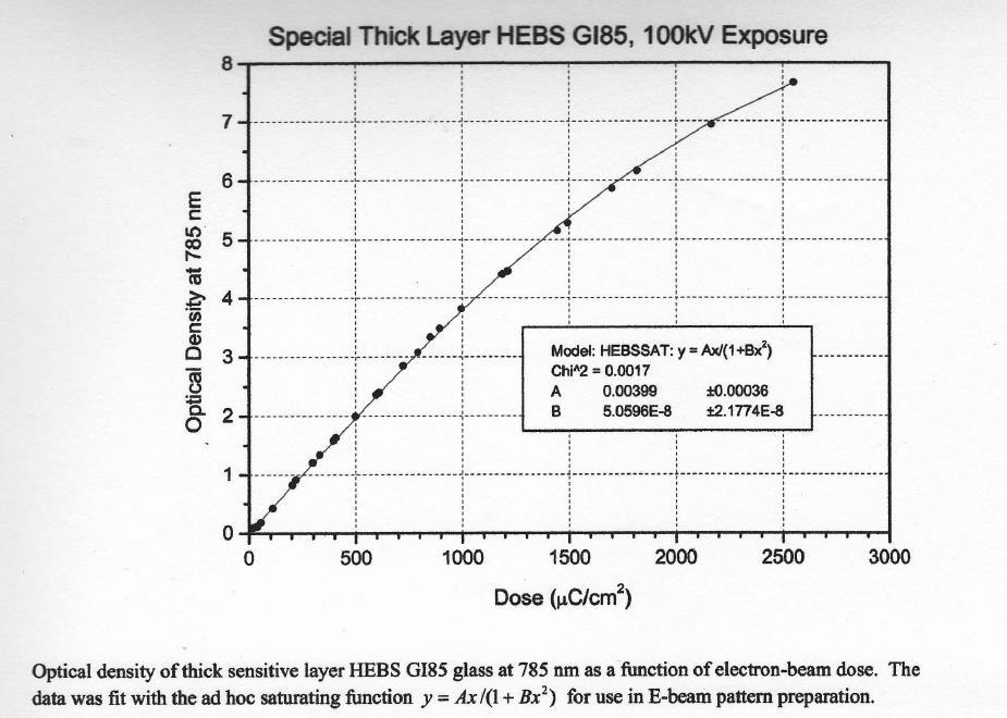
11 True Grayscale Photomask, A, is Essential to economic Mass Fabrication of 3D Microstructures, B A B 1. HBES-glass and LDW-glass photomasks enable mass production of 3D microstructures by spatially various exposure on photoresist 2. Convert optical density D(x,y) in a mask into designed height h(x,y) in a 3D microstructure 3. The microlens array shown here has many applications; see following slides 11
12 Fill Factor Enhancement of LCD s and Image Sensors In LCD displays, 70% of display area is blocked by TFT transistor circuit, microlens array is used to funnel light through each TFT transistor. In a detector array of an Image Sensor, 80% of a detector cell is blocked by electronic circuit, microlens array is used to focus light onto each detector cell 12

13 Microlens Array for Image Sensors SEM Micrograph of 60 micron lenslet array Atomic Force Micrograph of 5.5 micron Lenslet Array 13

14 Microlens Array for Wavefront Sensor Display on CCD 14

15 Wavefront Sensor in Adaptive Optics For Real Time Wavefront Correction 15

16 Random Phase Plate for Real Time Atmospheric Aberration Correction 16
 Devices An Example: Slider for Magnetic Hard Disc Drive")
17 Grayscale Micro Elements for Micro-Electro- Mechanical Systems (MEMS), and for Micro- Opto-Electro-Mechanical (MOEM) Devices An Example: Slider for Magnetic Hard Disc Drive 17
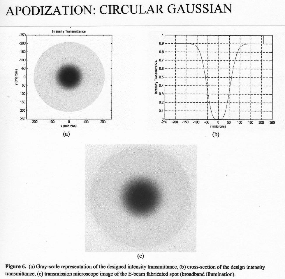
18 All-Glass Grayscale Photomasks Enable, i.e. DOE Having no coating of any kind, there exist no scattering from line edges, grayscale optical density patterns in an all-glass grayscale mask are faithfully and reproducibly converted into pre-designed gray scale height profiles in photoresists. 18
19 19
20 NASA Project Success to Look for Earth-like Planets Relies on HEBS-glass 20

21 HEBS-glass is the filter material of choice to look for an earth-like planet which is buried in the one billion time higher intensity background 21
22 ALL-Glass Gray Scale Photomasks Enable New Technologies A large number of publications exist world-wide including publications in technical journals, PhD dissertations, MS thesis, and patents by authors/inventors/companies/university professors/national labs throughout the world who rely on the use of HEBS-glass and/or LDW-glass grayscale photomasks to develop their new technologies 22
Applications of Maskless Lithography for the Production of Large Area Substrates Using the SF-100 ELITE. Jay Sasserath, PhD
 Applications of Maskless Lithography for the Production of Large Area Substrates Using the SF-100 ELITE Executive Summary Jay Sasserath, PhD Intelligent Micro Patterning LLC St. Petersburg, Florida Processing
Microlens formation using heavily dyed photoresist in a single step
 Microlens formation using heavily dyed photoresist in a single step Chris Cox, Curtis Planje, Nick Brakensiek, Zhimin Zhu, Jonathan Mayo Brewer Science, Inc., 2401 Brewer Drive, Rolla, MO 65401, USA ABSTRACT
Major Fabrication Steps in MOS Process Flow
 Major Fabrication Steps in MOS Process Flow UV light Mask oxygen Silicon dioxide photoresist exposed photoresist oxide Silicon substrate Oxidation (Field oxide) Photoresist Coating Mask-Wafer Alignment
Exhibit 2 Declaration of Dr. Chris Mack
 STC.UNM v. Intel Corporation Doc. 113 Att. 5 Exhibit 2 Declaration of Dr. Chris Mack Dockets.Justia.com UNITED STATES DISTRICT COURT DISTRICT OF NEW MEXICO STC.UNM, Plaintiff, v. INTEL CORPORATION Civil
CHAPTER 2 Principle and Design
 CHAPTER 2 Principle and Design The binary and gray-scale microlens will be designed and fabricated. Silicon nitride and photoresist will be taken as the material of the microlens in this thesis. The design
EG2605 Undergraduate Research Opportunities Program. Large Scale Nano Fabrication via Proton Lithography Using Metallic Stencils
 EG2605 Undergraduate Research Opportunities Program Large Scale Nano Fabrication via Proton Lithography Using Metallic Stencils Tan Chuan Fu 1, Jeroen Anton van Kan 2, Pattabiraman Santhana Raman 2, Yao
Part 5-1: Lithography
 Part 5-1: Lithography Yao-Joe Yang 1 Pattern Transfer (Patterning) Types of lithography systems: Optical X-ray electron beam writer (non-traditional, no masks) Two-dimensional pattern transfer: limited
Tolerancing microlenses using ZEMAX
 Tolerancing microlenses using ZEMAX Andrew Stockham, John G. Smith MEMS Optical *, Inc., 05 Import Circle, Huntsville, AL, USA 35806 ABSTRACT This paper demonstrates a new tolerancing technique that allows
Photolithography I ( Part 1 )
") 1 Photolithography I ( Part 1 ) Chapter 13 : Semiconductor Manufacturing Technology by M. Quirk & J. Serda Bjørn-Ove Fimland, Department of Electronics and Telecommunication, Norwegian University of Science
1 Photolithography I ( Part 1 ) Chapter 13 : Semiconductor Manufacturing Technology by M. Quirk & J. Serda Bjørn-Ove Fimland, Department of Electronics and Telecommunication, Norwegian University of Science
Micro- and Nano-Technology... for Optics
 Micro- and Nano-Technology...... for Optics 3.2 Lithography U.D. Zeitner Fraunhofer Institut für Angewandte Optik und Feinmechanik Jena Printing on Stones Map of Munich Stone Print Contact Printing light
Fabrication of suspended micro-structures using diffsuser lithography on negative photoresist
 Journal of Mechanical Science and Technology 22 (2008) 1765~1771 Journal of Mechanical Science and Technology www.springerlink.com/content/1738-494x DOI 10.1007/s12206-008-0601-8 Fabrication of suspended
OPTI510R: Photonics. Khanh Kieu College of Optical Sciences, University of Arizona Meinel building R.626
 OPTI510R: Photonics Khanh Kieu College of Optical Sciences, University of Arizona kkieu@optics.arizona.edu Meinel building R.626 Announcements Homework #3 is due today No class Monday, Feb 26 Pre-record
NANOFABRICATION, THE NEW GENERATION OF LITHOGRAPHY. Cheng-Sheng Huang & Alvin Chang ABSTRACT
 NANOFABRICATION, THE NEW GENERATION OF LITHOGRAPHY Cheng-Sheng Huang & Alvin Chang ABSTRACT Fabrication on the micro- and nano-structure has opened the new horizons in science and engineering. The success
Micro- and Nano-Technology... for Optics
 Micro- and Nano-Technology...... for Optics 3.2 Lithography U.D. Zeitner Fraunhofer Institut für Angewandte Optik und Feinmechanik Jena Printing on Stones Map of Munich Stone Print Shadow Printing Photomask
Semiconductor Manufacturing Technology. Semiconductor Manufacturing Technology. Photolithography: Resist Development and Advanced Lithography
 Semiconductor Manufacturing Technology Michael Quirk & Julian Serda October 2001 by Prentice Hall Chapter 15 Photolithography: Resist Development and Advanced Lithography Eight Basic Steps of Photolithography
NSERC Summer Project 1 Helping Improve Digital Camera Sensors With Prof. Glenn Chapman (ENSC)
") NSERC Summer 2016 Digital Camera Sensors & Micro-optic Fabrication ASB 8831, phone 778-782-319 or 778-782-3814, Fax 778-782-4951, email glennc@cs.sfu.ca http://www.ensc.sfu.ca/people/faculty/chapman/ Interested
NSERC Summer 2016 Digital Camera Sensors & Micro-optic Fabrication ASB 8831, phone 778-782-319 or 778-782-3814, Fax 778-782-4951, email glennc@cs.sfu.ca http://www.ensc.sfu.ca/people/faculty/chapman/ Interested
Project Staff: Timothy A. Savas, Michael E. Walsh, Thomas B. O'Reilly, Dr. Mark L. Schattenburg, and Professor Henry I. Smith
 9. Interference Lithography Sponsors: National Science Foundation, DMR-0210321; Dupont Agreement 12/10/99 Project Staff: Timothy A. Savas, Michael E. Walsh, Thomas B. O'Reilly, Dr. Mark L. Schattenburg,
Figure 7 Dynamic range expansion of Shack- Hartmann sensor using a spatial-light modulator
 Figure 4 Advantage of having smaller focal spot on CCD with super-fine pixels: Larger focal point compromises the sensitivity, spatial resolution, and accuracy. Figure 1 Typical microlens array for Shack-Hartmann
Fabrication Methodology of microlenses for stereoscopic imagers using standard CMOS process. R. P. Rocha, J. P. Carmo, and J. H.
 Fabrication Methodology of microlenses for stereoscopic imagers using standard CMOS process R. P. Rocha, J. P. Carmo, and J. H. Correia Department of Industrial Electronics, University of Minho, Campus
Innovative Mask Aligner Lithography for MEMS and Packaging
 Innovative Mask Aligner Lithography for MEMS and Packaging Dr. Reinhard Voelkel CEO SUSS MicroOptics SA September 9 th, 2010 1 SUSS Micro-Optics SUSS MicroOptics is a leading supplier for high-quality
A study on the fabrication method of middle size LGP using continuous micro-lenses made by LIGA reflow
 Korea-Australia Rheology Journal Vol. 19, No. 3, November 2007 pp. 171-176 A study on the fabrication method of middle size LGP using continuous micro-lenses made by LIGA reflow Jong Sun Kim, Young Bae
EE 143 Microfabrication Technology Fall 2014
 EE 143 Microfabrication Technology Fall 2014 Prof. Clark T.-C. Nguyen Dept. of Electrical Engineering & Computer Sciences University of California at Berkeley Berkeley, CA 94720 EE 143: Microfabrication
Feature-level Compensation & Control
 Feature-level Compensation & Control 2 Sensors and Control Nathan Cheung, Kameshwar Poolla, Costas Spanos Workshop 11/19/2003 3 Metrology, Control, and Integration Nathan Cheung, UCB SOI Wafers Multi wavelength
CMOS Digital Integrated Circuits Lec 2 Fabrication of MOSFETs
 CMOS Digital Integrated Circuits Lec 2 Fabrication of MOSFETs 1 CMOS Digital Integrated Circuits 3 rd Edition Categories of Materials Materials can be categorized into three main groups regarding their
Lecture 22 Optical MEMS (4)
") EEL6935 Advanced MEMS (Spring 2005) Instructor: Dr. Huikai Xie Lecture 22 Optical MEMS (4) Agenda: Refractive Optical Elements Microlenses GRIN Lenses Microprisms Reference: S. Sinzinger and J. Jahns,
EEL6935 Advanced MEMS (Spring 2005) Instructor: Dr. Huikai Xie Lecture 22 Optical MEMS (4) Agenda: Refractive Optical Elements Microlenses GRIN Lenses Microprisms Reference: S. Sinzinger and J. Jahns,
DOE Project: Resist Characterization
 DOE Project: Resist Characterization GOAL To achieve high resolution and adequate throughput, a photoresist must possess relatively high contrast and sensitivity to exposing radiation. The objective of
Photolithography Technology and Application
 Photolithography Technology and Application Jeff Tsai Director, Graduate Institute of Electro-Optical Engineering Tatung University Art or Science? Lind width = 100 to 5 micron meter!! Resolution = ~ 3
The Department of Advanced Materials Engineering. Materials and Processes in Polymeric Microelectronics
 The Department of Advanced Materials Engineering Materials and Processes in Polymeric Microelectronics 1 Outline Materials and Processes in Polymeric Microelectronics Polymeric Microelectronics Process
KMPR 1010 Process for Glass Wafers
 KMPR 1010 Process for Glass Wafers KMPR 1010 Steps Protocol Step System Condition Note Plasma Cleaning PVA Tepla Ion 10 5 mins Run OmniCoat Receipt Dehydration Any Heat Plate 150 C, 5 mins HMDS Coating
Semiconductor Technology
 Semiconductor Technology from A to Z + - x 1 0 x Photolithographie www.halbleiter.org Contents Contents List of Figures III 1 Photolithographie 1 1.1 Exposure and resist coating..........................
Fabrication of gray-scale masks and diffractive optical elements with LDW-glass
 Fabrication of gray-scale masks and diffractive optical elements with LDW-glass Victor Korolkov a, Anatoly Malyshev a, Alexander Poleshchuk a, Vadim Cherkashin a Hans J. Tiziani **b, Christof Pruß b, Thomas
Fabrication method of quartz aspheric microlens array for turning mask
 Opto-Electronic Engineering Article 018 45 4 1 1300 400714 Reactive ion etching Single point diamond turning Photoresist Glass substrate 5 mm 5 mm 1.155 nm 0.47% O439 A. [J]. 018 45(4): 170671 Fabrication
Fabrication of plastic microlens array using gas-assisted micro-hot-embossing with a silicon mold
 Infrared Physics & Technology 48 (2006) 163 173 www.elsevier.com/locate/infrared Fabrication of plastic microlens array using gas-assisted micro-hot-embossing with a silicon mold C.-Y. Chang a, S.-Y. Yang
EE-527: MicroFabrication
 EE-57: MicroFabrication Exposure and Imaging Photons white light Hg arc lamp filtered Hg arc lamp excimer laser x-rays from synchrotron Electrons Ions Exposure Sources focused electron beam direct write
Nanostencil Lithography and Nanoelectronic Applications
 Microsystems Laboratory Nanostencil Lithography and Nanoelectronic Applications Oscar Vazquez, Marc van den Boogaart, Dr. Lianne Doeswijk, Prof. Juergen Brugger, LMIS1 Dr. Chan Woo Park, Visiting Professor
Maskless Lithography Based on Digital Micro-Mirror Device (DMD) with Double Sided Microlens and Spatial Filter Array
 with Double Sided Microlens and Spatial Filter Array") 2017 2nd International Conference on Applied Mechanics, Electronics and Mechatronics Engineering (AMEME 2017) ISBN: 978-1-60595-497-4 Maskless Lithography Based on Digital Micro-Mirror Device (DMD) with
2017 2nd International Conference on Applied Mechanics, Electronics and Mechatronics Engineering (AMEME 2017) ISBN: 978-1-60595-497-4 Maskless Lithography Based on Digital Micro-Mirror Device (DMD) with
Microlens array-based exit pupil expander for full color display applications
 Proc. SPIE, Vol. 5456, in Photon Management, Strasbourg, France, April 2004 Microlens array-based exit pupil expander for full color display applications Hakan Urey a, Karlton D. Powell b a Optical Microsystems
Sidewall lithography of micron-sized features in high-aspect-ratio meso-scale channels using a three-dimensional assembled mask
 Ji et al. Micro and Nano Systems Letters 2014, 2:6 LETTER Open Access Sidewall lithography of micron-sized features in high-aspect-ratio meso-scale channels using a three-dimensional assembled mask Chang-Hyeon
Lesson Plan Title Primary Subject Area Grade Level Overview Approximate Duration MA Frameworks Interdisciplinary Connections Lesson Objectives
 Lesson Plan Title Screenprinting/photolithography and understanding MEMS production and their application Primary Subject Area Chemistry Grade Level High School (10) Overview Students will learn about
Integrated Focusing Photoresist Microlenses on AlGaAs Top-Emitting VCSELs
 Integrated Focusing Photoresist Microlenses on AlGaAs Top-Emitting VCSELs Andrea Kroner We present 85 nm wavelength top-emitting vertical-cavity surface-emitting lasers (VCSELs) with integrated photoresist
Pattern Transfer CD-AFM. Resist Features on Poly. Poly Features on Oxide. Quate Group, Stanford University
 Resist Features on Poly Pattern Transfer Poly Features on Oxide CD-AFM The Critical Dimension AFM Boot -Shaped Tip Tip shape is optimized to sense topography on vertical surfaces Two-dimensional feedback
Technology for the MEMS processing and testing environment. SUSS MicroTec AG Dr. Hans-Georg Kapitza
 Technology for the MEMS processing and testing environment SUSS MicroTec AG Dr. Hans-Georg Kapitza 1 SUSS MicroTec Industrial Group Founded 1949 as Karl Süss KG GmbH&Co. in Garching/ Munich San Jose Waterbury
Nanonics Systems are the Only SPMs that Allow for On-line Integration with Standard MicroRaman Geometries
 Nanonics Systems are the Only SPMs that Allow for On-line Integration with Standard MicroRaman Geometries 2002 Photonics Circle of Excellence Award PLC Ltd, England, a premier provider of Raman microspectral
EUVL Activities in China. Xiangzhao Wang Shanghai Inst. Of Opt. and Fine Mech. Of CAS. (SIOM) Shanghai, China.
 Shanghai, China.") EUVL Activities in China Xiangzhao Wang Shanghai Inst. Of Opt. and Fine Mech. Of CAS. (SIOM) Shanghai, China. wxz26267@siom.ac.cn Projection Optics Imaging System Surface Testing Optical Machining ML Coating
EUVL Activities in China Xiangzhao Wang Shanghai Inst. Of Opt. and Fine Mech. Of CAS. (SIOM) Shanghai, China. wxz26267@siom.ac.cn Projection Optics Imaging System Surface Testing Optical Machining ML Coating
Lecture 15. Lecture 15
 Lecture 15 Charge coupled device (CCD) The basic CCD is composed of a linear array of MOS capacitors. It functions as an analog memory and shift register. The operation is indicated in the diagram below:
Snapshot Mask-less fabrication of embedded monolithic SU-8 microstructures with arbitrary topologies
 Snapshot Mask-less fabrication of embedded monolithic SU-8 microstructures with arbitrary topologies Pakorn Preechaburana and Daniel Filippini Linköping University Post Print N.B.: When citing this work,
32nm High-K/Metal Gate Version Including 2nd Generation Intel Core processor family
 From Sand to Silicon Making of a Chip Illustrations 32nm High-K/Metal Gate Version Including 2nd Generation Intel Core processor family April 2011 1 The illustrations on the following foils are low resolution
Outline. 1 Introduction. 2 Basic IC fabrication processes. 3 Fabrication techniques for MEMS. 4 Applications. 5 Mechanics issues on MEMS MDL NTHU
 Outline 1 Introduction 2 Basic IC fabrication processes 3 Fabrication techniques for MEMS 4 Applications 5 Mechanics issues on MEMS 2.2 Lithography Reading: Runyan Chap. 5, or 莊達人 Chap. 7, or Wolf and
Lasers Defect Correction in DRAM's Problem: very hard to make memory chips with no defects Memory chips have maximum density of devices Repeated
 Lasers Defect Correction in DRAM's Problem: very hard to make memory chips with no defects Memory chips have maximum density of devices Repeated structures all substitutable Create spare rows and columns
MEMS in ECE at CMU. Gary K. Fedder
 MEMS in ECE at CMU Gary K. Fedder Department of Electrical and Computer Engineering and The Robotics Institute Carnegie Mellon University Pittsburgh, PA 15213-3890 fedder@ece.cmu.edu http://www.ece.cmu.edu/~mems
Hermetic Packaging Solutions using Borosilicate Glass Thin Films. Lithoglas Hermetic Packaging Solutions using Borosilicate Glass Thin Films
 Hermetic Packaging Solutions using Borosilicate Glass Thin Films 1 Company Profile Company founded in 2006 ISO 9001:2008 qualified since 2011 Headquarters and Production in Dresden, Germany Production
5. Lithography. 1. photolithography intro: overall, clean room 2. principle 3. tools 4. pattern transfer 5. resolution 6. next-gen
 5. Lithography 1. photolithography intro: overall, clean room 2. principle 3. tools 4. pattern transfer 5. resolution 6. next-gen References: Semiconductor Devices: Physics and Technology. 2 nd Ed. SM
Virtual input device with diffractive optical element
 Virtual input device with diffractive optical element Ching Chin Wu, Chang Sheng Chu Industrial Technology Research Institute ABSTRACT As a portable device, such as PDA and cell phone, a small size build
Nanofluidic Diodes based on Nanotube Heterojunctions
 Supporting Information Nanofluidic Diodes based on Nanotube Heterojunctions Ruoxue Yan, Wenjie Liang, Rong Fan, Peidong Yang 1 Department of Chemistry, University of California, Berkeley, CA 94720, USA
ICMIEE Generation of Various Micropattern Using Microlens Projection Photolithography
 International Conference on Mechanical, Industrial and Energy Engineering 2014 26-27 December, 2014, Khulna, BANGLADESH Generation of Various Micropattern Using Microlens Projection Photolithography Md.
State-of-the-art device fabrication techniques
 State-of-the-art device fabrication techniques! Standard Photo-lithography and e-beam lithography! Advanced lithography techniques used in semiconductor industry Deposition: Thermal evaporation, e-gun
Two step process for the fabrication of diffraction limited concave microlens arrays
 Two step process for the fabrication of diffraction limited concave microlens arrays Patrick Ruffieux 1*, Toralf Scharf 1, Irène Philipoussis 1, Hans Peter Herzig 1, Reinhard Voelkel 2, and Kenneth J.
A BASIC EXPERIMENTAL STUDY OF CAST FILM EXTRUSION PROCESS FOR FABRICATION OF PLASTIC MICROLENS ARRAY DEVICE
 A BASIC EXPERIMENTAL STUDY OF CAST FILM EXTRUSION PROCESS FOR FABRICATION OF PLASTIC MICROLENS ARRAY DEVICE Chih-Yuan Chang and Yi-Min Hsieh and Xuan-Hao Hsu Department of Mold and Die Engineering, National
Nanomanufacturing and Fabrication By Matthew Margolis
 Nanomanufacturing and Fabrication By Matthew Margolis Manufacturing is the transformation of raw materials into finished goods for sale, or intermediate processes involving the production or finishing
Micro-Nanofabrication
 Zheng Cui Micro-Nanofabrication TECHNOLOGIES AND APPLICATIONS ^f**"?* ö Springer Higher Education Press -T O Table of Content Preface About the Author Chapter 1 Introduction 1 1.1 Micro-nanotechnologies
Design Rules for Silicon Photonics Prototyping
 Design Rules for licon Photonics Prototyping Version 1 (released February 2008) Introduction IME s Photonics Prototyping Service offers 248nm lithography based fabrication technology for passive licon-on-insulator
Lithography. 3 rd. lecture: introduction. Prof. Yosi Shacham-Diamand. Fall 2004
 Lithography 3 rd lecture: introduction Prof. Yosi Shacham-Diamand Fall 2004 1 List of content Fundamental principles Characteristics parameters Exposure systems 2 Fundamental principles Aerial Image Exposure
The End of Thresholds: Subwavelength Optical Linewidth Measurement Using the Flux-Area Technique
 The End of Thresholds: Subwavelength Optical Linewidth Measurement Using the Flux-Area Technique Peter Fiekowsky Automated Visual Inspection, Los Altos, California ABSTRACT The patented Flux-Area technique
Chapter 3 Fabrication
 Chapter 3 Fabrication The total structure of MO pick-up contains four parts: 1. A sub-micro aperture underneath the SIL The sub-micro aperture is used to limit the final spot size from 300nm to 600nm for
MicroPG 101 Pattern Generator Standard Operating Procedure Draft v.0.2
 Tool owner: Roman Akhmechet, romana@princeton.edu, x 8-0468 Backup: David Barth, dbarth@princeton.edu MicroPG 101 Pattern Generator Standard Operating Procedure Draft v.0.2 QUICK GUIDE PROCEDURE OVERVIEW
Fabrication of micro structures on curve surface by X-ray lithography
 Fabrication of micro structures on curve surface by X-ray lithography Yigui Li 1, Susumu Sugiyama 2 Abstract We demonstrate experimentally the x-ray lithography techniques to fabricate micro structures
Chapter 2 Silicon Planar Processing and Photolithography
 Chapter 2 Silicon Planar Processing and Photolithography The success of the electronics industry has been due in large part to advances in silicon integrated circuit (IC) technology based on planar processing,
Nanomanufacturing and Fabrication
 Nanomanufacturing and Fabrication Matthew Margolis http://www.cnm.es/im b/pages/services/im ages/nanofabrication%20laboratory_archivos/im age007.jpg What we will cover! Definitions! Top Down Vs Bottom
Clean Room Technology Optical Lithography. Lithography I. takenfrombdhuey
 Clean Room Technology Optical Lithography Lithography I If the automobile had followed the same development cycle as the computer, a Rolls Royce would today cost $100, get a million miles per gallon, and
Rapid and inexpensive fabrication of polymeric microfluidic devices via toner transfer masking
 Easley et al. Toner Transfer Masking Page -1- B816575K_supplementary_revd.doc December 3, 2008 Supplementary Information for Rapid and inexpensive fabrication of polymeric microfluidic devices via toner
Module - 2 Lecture - 13 Lithography I
 Nano Structured Materials-Synthesis, Properties, Self Assembly and Applications Prof. Ashok. K.Ganguli Department of Chemistry Indian Institute of Technology, Delhi Module - 2 Lecture - 13 Lithography
Simulation of High Resistivity (CMOS) Pixels
 Pixels") Simulation of High Resistivity (CMOS) Pixels Stefan Lauxtermann, Kadri Vural Sensor Creations Inc. AIDA-2020 CMOS Simulation Workshop May 13 th 2016 OUTLINE 1. Definition of High Resistivity Pixel Also
Simulation of High Resistivity (CMOS) Pixels Stefan Lauxtermann, Kadri Vural Sensor Creations Inc. AIDA-2020 CMOS Simulation Workshop May 13 th 2016 OUTLINE 1. Definition of High Resistivity Pixel Also
NanoFabrication Kingston. Seminar and Webinar January 31, 2017 Rob Knobel Associate Professor, Dept. of Physics Queen s University
 NanoFabrication Kingston Seminar and Webinar January 31, 2017 Rob Knobel Associate Professor, Dept. of Physics Queen s University What is NFK? It s a place, an team of experts and a service. The goal of
Results of Proof-of-Concept 50keV electron multi-beam Mask Exposure Tool (emet POC)
") Results of Proof-of-Concept 50keV electron multi-beam Mask Exposure Tool (emet POC) Elmar Platzgummer *, Christof Klein, and Hans Loeschner IMS Nanofabrication AG Schreygasse 3, A-1020 Vienna, Austria
Results of Proof-of-Concept 50keV electron multi-beam Mask Exposure Tool (emet POC) Elmar Platzgummer *, Christof Klein, and Hans Loeschner IMS Nanofabrication AG Schreygasse 3, A-1020 Vienna, Austria
Dr. Dirk Meyners Prof. Wagner. Wagner / Meyners Micro / Nanosystems Technology
 Micro/Nanosystems Technology Dr. Dirk Meyners Prof. Wagner 1 Outline - Lithography Overview - UV-Lithography - Resolution Enhancement Techniques - Electron Beam Lithography - Patterning with Focused Ion
50 YEARS SUSS MASK ALIGNER
 50 YEARS SUSS MASK ALIGNER Ralph Zoberbier SUSS MicroTec Lithography GmbH Germany Published in the SUSS report 01/2013 E-mail: info@suss.com www.suss.com 50 YEARS SUSS MASK ALIGNER Ralph Zoberbier SUSS
MICRO AND NANOPROCESSING TECHNOLOGIES
 MICRO AND NANOPROCESSING TECHNOLOGIES LECTURE 4 Optical lithography Concepts and processes Lithography systems Fundamental limitations and other issues Photoresists Photolithography process Process parameter
2 Integrated Circuit Manufacturing:
 2 Integrated Circuit Manufacturing: A Technology Resource 2 IC MANUFACTURING TECHNOLOGIES While the integrated circuit drives the packaging and assembly, the IC manufacturing process, and associated methodologies,
(12) Patent Application Publication (10) Pub. No.: US 2003/ A1
 Patent Application Publication (10) Pub. No.: US 2003/ A1") US 20030091084A1 (19) United States (12) Patent Application Publication (10) Pub. No.: US 2003/0091084A1 Sun et al. (43) Pub. Date: May 15, 2003 (54) INTEGRATION OF VCSEL ARRAY AND Publication Classification
US 20030091084A1 (19) United States (12) Patent Application Publication (10) Pub. No.: US 2003/0091084A1 Sun et al. (43) Pub. Date: May 15, 2003 (54) INTEGRATION OF VCSEL ARRAY AND Publication Classification
ML² Multi Layer Micro Lab
 Deliverable 4.5 ML² Multi Layer Micro Lab D4.5 - Report on product range for UV curing lacquers, validated for ML² devices 1. Introduction... 2 2. UV embossing lacquer chemistry... 2 2.1. The main components
Pulsed Laser Ablation of Polymers for Display Applications
 Pulsed Laser Ablation of Polymers for Display Applications James E.A Pedder 1, Andrew S. Holmes 2, Heather J. Booth 1 1 Oerlikon Optics UK Ltd, Oxford Industrial Estate, Yarnton, Oxford, OX5 1QU, UK 2
IMAGING SILICON NANOWIRES
 Project report IMAGING SILICON NANOWIRES PHY564 Submitted by: 1 Abstract: Silicon nanowires can be easily integrated with conventional electronics. Silicon nanowires can be prepared with single-crystal
A new class of LC-resonator for micro-magnetic sensor application
 Journal of Magnetism and Magnetic Materials 34 (26) 117 121 www.elsevier.com/locate/jmmm A new class of LC-resonator for micro-magnetic sensor application Yong-Seok Kim a, Seong-Cho Yu a, Jeong-Bong Lee
Samsung LTN097QL01-A01 Display Module with LED Backlit LCD and Capacitive Touch Screen
 Samsung LTN097QL01-A01 Display Module with LED Backlit LCD and Capacitive Touch Screen From the Retina Display in the New ipad, Also Known As the ipad 3 Released by Apple in March, 2012 Custom Display
Advanced 3D Optical Profiler using Grasshopper3 USB3 Vision camera
 Advanced 3D Optical Profiler using Grasshopper3 USB3 Vision camera Figure 1. The Zeta-20 uses the Grasshopper3 and produces true color 3D optical images with multi mode optics technology 3D optical profiling
Half-tone proximity lithography
 Half-tone proximity lithography Torsten Harzendorf* a, Lorenz Stuerzebecher a, Uwe Vogler b, Uwe D. Zeitner a, Reinhard Voelkel b a Fraunhofer Institut für Angewandte Optik und Feinmechanik IOF, Albert
The Development of Device Lithography
 5 66 PROCEEDINGS OF THE IEEE, VOL. 71, NO. 5, MAY 1983 The Development of Device Lithography DONALD R. HERRIOT", SENIOR MEMBER, IEEE Invited Paper Abstmet-Lithography has been the principal pacing element
write-nanocircuits Direct-write Jaebum Joo and Joseph M. Jacobson Molecular Machines, Media Lab Massachusetts Institute of Technology, Cambridge, MA
 Fab-in in-a-box: Direct-write write-nanocircuits Jaebum Joo and Joseph M. Jacobson Massachusetts Institute of Technology, Cambridge, MA April 17, 2008 Avogadro Scale Computing / 1 Avogadro number s? Intel
Module 11: Photolithography. Lecture11: Photolithography - I
 Module 11: Photolithography Lecture11: Photolithography - I 1 11.0 Photolithography Fundamentals We will all agree that incredible progress is happening in the filed of electronics and computers. For example,
This writeup is adapted from Fall 2002, final project report for by Robert Winsor.
 Optical Waveguides in Andreas G. Andreou This writeup is adapted from Fall 2002, final project report for 520.773 by Robert Winsor. September, 2003 ABSTRACT This lab course is intended to give students
Ion Beam Lithography: faster writing strategies for features between 150nm and 1um
 Ion Beam Lithography: faster writing strategies for features between 150nm and 1um Brent P. Gila, Andes Trucco, David Hays Located in sunny Gainesville, FL (100 miles north of Disney World) https://nrf.aux.eng.ufl.edu/
University of Arizona Optical Sciences Center High Speed Maskless Lithography Phototool
 University of Arizona Optical Sciences Center High Speed Maskless Lithography Phototool EXECUTIVE SUMMARY Introduction Maskless lithography (ML) has wide applications, from next-generation semiconductor
Photolithography 光刻 Part I: Optics
 微纳光电子材料与器件工艺原理 Photolithography 光刻 Part I: Optics Xing Sheng 盛兴 Department of Electronic Engineering Tsinghua University xingsheng@tsinghua.edu.cn 1 Integrate Circuits Moore's law transistor number transistor
Wavefront sensor sampling plane fabricated by maskless grayscale lithography
 Wavefront sensor sampling plane fabricated by maskless grayscale lithography G.A. Cirino * a, F.T. Amaral b, S.A. Lopera c, A.N. Montagnolil a, A. Arruda d, R.D. Mansano c, T.M-Brahim e, D.W.L. Monteiro
Machine-Aligned Fabrication of Submicron SIS Tunnel Junctions Using a Focused Ion Beam
 Machine-Aligned Fabrication of Submicron SIS Tunnel Junctions Using a Focused Ion Beam Robert. B. Bass, Jian. Z. Zhang and Aurthur. W. Lichtenberger Department of Electrical Engineering, University of
Rapid fabrication of ultraviolet-cured polymer microlens arrays by soft roller stamping process
 Microelectronic Engineering 84 (2007) 355 361 www.elsevier.com/locate/mee Rapid fabrication of ultraviolet-cured polymer microlens arrays by soft roller stamping process Chih-Yuan Chang, Sen-Yeu Yang *,
U.S. Air Force Phillips hboratoq, Kirtland AFB, NM 87117, 505/ , FAX:
 Evaluation of Wavefront Sensors Based on Etched R. E. Pierson, K. P. Bishop, E. Y. Chen Applied Technology Associates, 19 Randolph SE, Albuquerque, NM 8716, SOS/846-61IO, FAX: 59768-1391 D. R. Neal Sandia
DIY fabrication of microstructures by projection photolithography
 DIY fabrication of microstructures by projection photolithography Andrew Zonenberg Rensselaer Polytechnic Institute 110 8th Street Troy, New York U.S.A. 12180 zonena@cs.rpi.edu April 20, 2011 Abstract
Curriculum Vitae. (Some of my experiences after 2003 & certifications are shown on the website)
") Curriculum Vitae Dr. Wang Qin Born: Nationality: E-mail: October, 1967, Zhejiang Province, China Singapore qwangabcd@gmail.com Hand phone: 65-84637402 Personal website: http://wangqinsite.weebly.com (Some
Curriculum Vitae Dr. Wang Qin Born: Nationality: E-mail: October, 1967, Zhejiang Province, China Singapore qwangabcd@gmail.com Hand phone: 65-84637402 Personal website: http://wangqinsite.weebly.com (Some
Photolithography II ( Part 2 )
") 1 Photolithography II ( Part 2 ) Chapter 14 : Semiconductor Manufacturing Technology by M. Quirk & J. Serda Saroj Kumar Patra, Department of Electronics and Telecommunication, Norwegian University of Science
1 Photolithography II ( Part 2 ) Chapter 14 : Semiconductor Manufacturing Technology by M. Quirk & J. Serda Saroj Kumar Patra, Department of Electronics and Telecommunication, Norwegian University of Science