Lithography. 3 rd. lecture: introduction. Prof. Yosi Shacham-Diamand. Fall 2004
|
|
|
- Charlene Wilkerson
- 6 years ago
- Views:
Transcription
1 Lithography 3 rd lecture: introduction Prof. Yosi Shacham-Diamand Fall
2 List of content Fundamental principles Characteristics parameters Exposure systems 2
3 Fundamental principles Aerial Image Exposure Development Critical dimension (CD) control 3
4 Lithography characterization Post exposure characterization Line-width control, photo-resist profile, resolution, process window Registration Process compatibility Etch resistance, thermal stability, adhesion, chemical compatibility, resist removal Manufacturability Cost, safety, defects, stability, shelf life 4
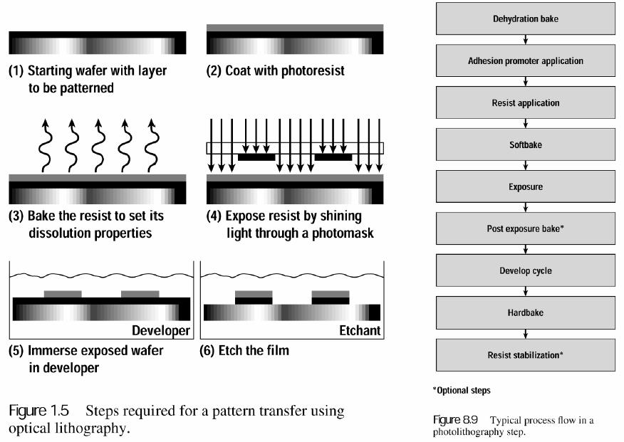
5 Lithography: information transfer process Mask Design Optical image Latent image in the photo-lithographic material Image development Transfer onto the wafer 5
6 6
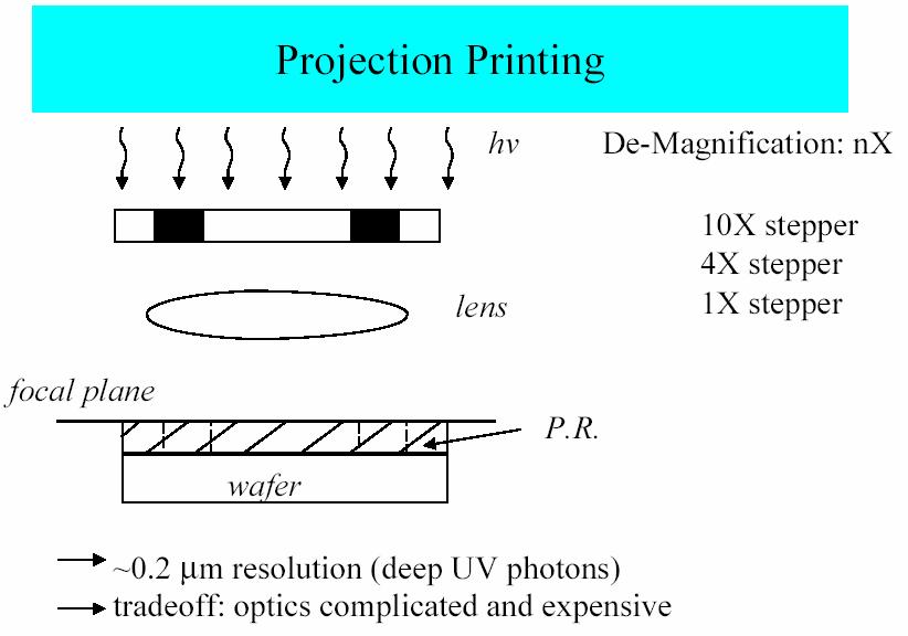
7 Image transfer from the mask to the wafer UV light source Shutter Alignment laser Shutter is closed during focus and alignment and removed during wafer exposure Reticle (may contain one or more die in the reticle field) Single field exposure, includes: focus, align, expose, step, and repeat process 7 Figure 14.1 Projection lens (reduces the size of reticle field for presentation to the wafer surface) Wafer stage controls position of wafer in X, Y, Z, θ
8 8
9 Typical CMOS masks 1) STI etch 2) P-well implant 3) N-well implant 4) Poly gate etch 5) N + S/D implant 6) P + S/D implant 7) Oxide contact etch 8) Metal etch Resulting layers Cross section 9 Top view
10 10
11 11
12 12
13 13
14 14
15 15
16 16
17 17
18 18
19 19
20 Exposure systems Mask illumination from the backside The light interacts with the mask The electromagnetic wave reaches the lens The lens collects part of the light and forms and image on the wafer There is an information loss due to the finite size of the lens 20
21 Light an electromagnetic wave phenomena λ = v f λ v = velocity of light, 3 x10 8 m/sec f = frequency in Hertz (cycles per second) λ = wavelength, the physical length of one cycle of a frequency, expressed in meters Laser 21
22 Constructive Diffraction Destructive A Destructive Waves in phase Waves Waves out of phase out of phase B A+B 22
23 Optical filtering Broadband light Reflected wavelengths Coating 1 (non-reflecting) Coating 2 Secondary reflections (interference) Coating 3 Glass 23 Transmitted wavelength
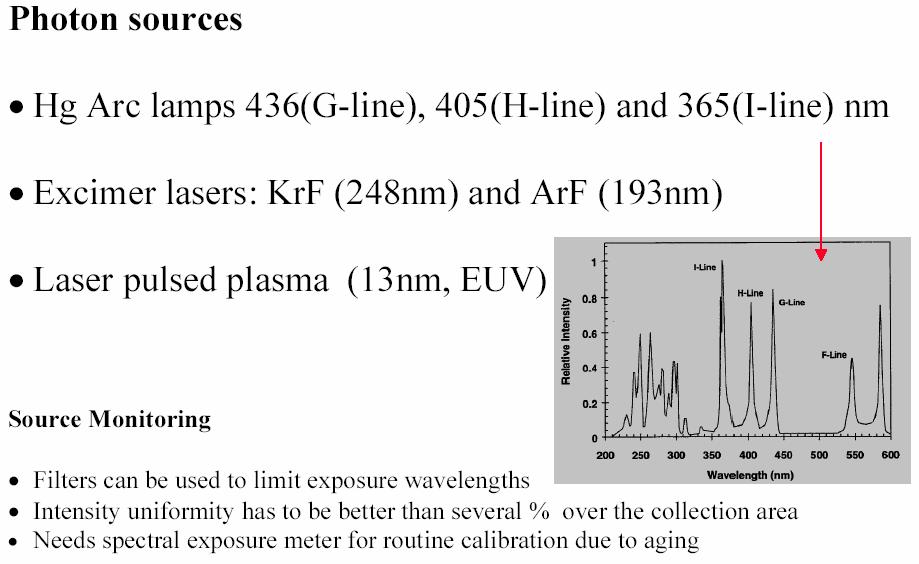
24 UV Spectrum λ (nm) Ultraviolet spectrum Visible spectrum EUV VUV DUV Mid-UV Violet Blue Green YellowOrange Red i h g Excimer laser Mercury lamp 24 Photolithography light sources
25 25
26 High pressure Hg lamp Emission spectrum of high-intensity mercury lamp i-line 365 nm Relative Intensity (%) DUV 248 nm h-line 405 nm g-line 436 nm Wavelength (nm)
27 High pressure Hg lamp UV Light Wavelength (nm) Descriptor CD Resolution (µm) 436 g-line h-line i-line Deep UV (DUV)
28 Hg lamp vs. Excimer laser 100 KrF laser Relative Intensity (%) Hg lamp Wavelength (nm)
29 29
30 Resist UV absorption Photoresist (after develop) Sloping profile Substrate 30
31 Eximer lasers for lithography Material Wavelengt h (nm) Max. Output (mj/pulse) Frequency (pulses/sec) Pulse Length (ns) CD Resolution (µm) KrF ArF F
32 Spatial Coherence Incoherent light source Black box illuminator of a single wavelength Slit Two slits closely spaced Interference patterns Coherent cylindrical wave front Two coherent cylindrical wave fronts 32
33 Optical lithography Optics Reflection Refraction Lens Diffraction Typical parameters 33
34 Reflection laws The angle of incidence of a light wavefront with a plane mirror is equal to the angle of reflection. Incident light θ i θ r Reflected light 34 Law of Reflection: θ i = θ r
35 Reflection lithography Flat mirror Illuminator for a simple aligner Ellipsoidal mirror Mask Flat mirror 35
36 Refraction Snell s Law: sin θ i = n sin θ r Index of refraction, n = sin θ i / sin θ r fast medium air (n 1.0) slow medium glass (n = 1.5) glass (n = 1.5) θ slow medium air (n 1.0) θ fast medium 36
37 Refraction index Material Index of Refraction (n) Air Water 1.33 Fused Silica (Amorphous Quartz) Diamond
38 Lens based lithography Illuminator assembly Optical filter Shutter Mercury lamp Masking unit Condenser lens Fly s eye lens Flat mirror Light sensor Mirror Condenser lens Mirror Collimator lens Reticle Reticle stage (X, Y, θ) Lamp monitor Lamp position knob Ellipsoidal mirror Fiber optics X-drive motor Projection optics Optical focus sensor Interferometer mirror θ-z drive stage Y-drive motor Vacuum chuck Wafer stage assembly 38
39 Converging lens 2f f f = focal length F = focal point S = 2f O = origin, center of lens S Object Real F O F image S 39
40 Diverging lens S Object Virtua l image f = focal length F = focal point S = 2f O = origin, center of lens F O F S 40
41 Laser-Induced Lens Compaction Compacted area of lens 41
42 Interference Pattern from Light Diffraction at Small Opening Light travels in straight lines. Diffraction occurs when light hits edges of objects. Diffraction bands, or interference patterns, occur when light waves pass through narrow slits. 42 Diffraction bands
43 Diffraction in a Reticle Pattern Diffracted light rays Slit Plane light wave 43

44 44 Bragg s condition for constructive diffraction
45 Lens Capturing Diffracted Light Quartz UV Mask Chrome Diffraction patterns Lens 45

46 Effect of Numerical Aperture on Imaging Pinhole masks Lens NA Image results Bad Exposure light Poor Good 46 Diffracted light
47 Image formation - example Coherent illumination Quartz plate with chromium pattern with a periodicity (pitch) of p. θn Bragg s law p sin(θ n ) = nλ 47
48 The lens Lens with diameter D & distance f from the focal plane NA = nsin( α) D 2 f 48 Mask Focal plane
49 49
50 50
51 51
52 52
53 53
54 Typical NA Values for Photolithography Tools Type of Equipment Scanning Projection Aligner with mirrors (1970s technology) NA Value 0.25 Step-and-Repeat Step-and-Scan
55 What determines the resolution? The resolution is proportional to the wavelength, λ The resolution is proportional to the numerical aperture, NA; larger lens collects more information. Re solution = k 1 λ NA 55
56 56
 and")
57 57 Definition of line-width (L) and line-spacing (S)
58 Image contrast Intensity, I 1 I max I min 0 Image contrast = I I max max - I + I min min 58
59 59
60 60
61 The limitations of the optical contrast as a figure of merit It represents only an image of a simple pattern with lines and spaces Not practical for large or complex features Too sensitive to the minimum intensity than the real image Low correlation to the lithography quality. 61
62 62
63 Photoresist Reflective Notching Due to Light Reflections UV exposure light Mask Edge diffraction Exposed photoresist Polysilicon Unexposed photoresist Notched photoresist Surface reflection STI Substrate STI 63
64 Incident and Reflected Light Wave Interference in Photoresist Incident wave Reflected wave Photoresist Film Substrate 64 Standing waves cause nonuniform exposure along the thickness of the photoresist film.

65 65 Standing waves in the resist
66 Solution Anti Reflective Coating (ARC) Incident wave Antireflective coating Photoresist Film Substrate 66 The use of antireflective coatings, dyes, and filters can help prevent interference.
67 BARC - Bottom Antireflective Coating UV exposure light Mask 67 Exposed photoresist Polysilicon STI Unexposed photoresist BARC Substrate STI
68 BARC Phase-Shift Cancellation of Light (A) Incident light (B) Top surface reflection (C) (D) Photoresist BARC (TiN) Aluminum C and D cancel due to phase difference 68
69 Top Antireflective Coating Incident light Resist-substrate reflections Incident light Top antireflective coating absorbs substrate reflections. Photoresist Photoresist Substrate reflection Substrate Substrate 69
70 Optical Lithography Resolution Calculating Resolution Depth of Focus Resolution Versus Depth of Focus Surface Planarity 70
71 Resolution of Features The dimensions of linewidths and spaces must be equal. As feature sizes decrease, it is more difficult to separate features from each other
72 Calculating Resolution for a given λ, NA and k k = 0.6 Illuminator, λ R = k λ NA Mask Lens, NA Wafer R i-line DUV λ ΝΑ R 365 nm nm 365 nm nm 193 nm nm 193 nm nm 72
73 Depth of Focus (DOF) Lens Center of focus - Depth of focus Photoresist + Film 73
74 74
75 75
76 Example to focal plane problems due to a non-planar surface 76
77 77
78 78
79 79
80 Resolution Versus Depth of Focus for Varying NA DOF = λ 2(NA) 2 Illuminator, λ Mask i-line DUV λ ΝΑ R DOF 365 nm nm 901 nm 365 nm nm 507 nm 193 nm nm 476 nm 193 nm nm 268 nm Lens, NA Center of focus - Depth of focus Photoresist Wafer DOF + Film 80

81 New approaches super resolution imaging 81
Photolithography II ( Part 2 )
") 1 Photolithography II ( Part 2 ) Chapter 14 : Semiconductor Manufacturing Technology by M. Quirk & J. Serda Saroj Kumar Patra, Department of Electronics and Telecommunication, Norwegian University of Science
1 Photolithography II ( Part 2 ) Chapter 14 : Semiconductor Manufacturing Technology by M. Quirk & J. Serda Saroj Kumar Patra, Department of Electronics and Telecommunication, Norwegian University of Science
Section 2: Lithography. Jaeger Chapter 2. EE143 Ali Javey Slide 5-1
 Section 2: Lithography Jaeger Chapter 2 EE143 Ali Javey Slide 5-1 The lithographic process EE143 Ali Javey Slide 5-2 Photolithographic Process (a) (b) (c) (d) (e) (f) (g) Substrate covered with silicon
Section 2: Lithography. Jaeger Chapter 2 Litho Reader. The lithographic process
 Section 2: Lithography Jaeger Chapter 2 Litho Reader The lithographic process Photolithographic Process (a) (b) (c) (d) (e) (f) (g) Substrate covered with silicon dioxide barrier layer Positive photoresist
Photolithography I ( Part 1 )
") 1 Photolithography I ( Part 1 ) Chapter 13 : Semiconductor Manufacturing Technology by M. Quirk & J. Serda Bjørn-Ove Fimland, Department of Electronics and Telecommunication, Norwegian University of Science
1 Photolithography I ( Part 1 ) Chapter 13 : Semiconductor Manufacturing Technology by M. Quirk & J. Serda Bjørn-Ove Fimland, Department of Electronics and Telecommunication, Norwegian University of Science
Section 2: Lithography. Jaeger Chapter 2 Litho Reader. EE143 Ali Javey Slide 5-1
 Section 2: Lithography Jaeger Chapter 2 Litho Reader EE143 Ali Javey Slide 5-1 The lithographic process EE143 Ali Javey Slide 5-2 Photolithographic Process (a) (b) (c) (d) (e) (f) (g) Substrate covered
MICROCHIP MANUFACTURING by S. Wolf
 MICROCHIP MANUFACTURING by S. Wolf Chapter 19 LITHOGRAPHY II: IMAGE-FORMATION and OPTICAL HARDWARE 2004 by LATTICE PRESS CHAPTER 19 - CONTENTS Preliminaries: Wave- Motion & The Behavior of Light Resolution
Part 5-1: Lithography
 Part 5-1: Lithography Yao-Joe Yang 1 Pattern Transfer (Patterning) Types of lithography systems: Optical X-ray electron beam writer (non-traditional, no masks) Two-dimensional pattern transfer: limited
EE143 Fall 2016 Microfabrication Technologies. Lecture 3: Lithography Reading: Jaeger, Chap. 2
 EE143 Fall 2016 Microfabrication Technologies Lecture 3: Lithography Reading: Jaeger, Chap. 2 Prof. Ming C. Wu wu@eecs.berkeley.edu 511 Sutardja Dai Hall (SDH) 1-1 The lithographic process 1-2 1 Photolithographic
Major Fabrication Steps in MOS Process Flow
 Major Fabrication Steps in MOS Process Flow UV light Mask oxygen Silicon dioxide photoresist exposed photoresist oxide Silicon substrate Oxidation (Field oxide) Photoresist Coating Mask-Wafer Alignment
Lecture 7. Lithography and Pattern Transfer. Reading: Chapter 7
 Lecture 7 Lithography and Pattern Transfer Reading: Chapter 7 Used for Pattern transfer into oxides, metals, semiconductors. 3 types of Photoresists (PR): Lithography and Photoresists 1.) Positive: PR
ECSE 6300 IC Fabrication Laboratory Lecture 3 Photolithography. Lecture Outline
 ECSE 6300 IC Fabrication Laboratory Lecture 3 Photolithography Prof. James J. Q. Lu Bldg. CII, Rooms 6229 Rensselaer Polytechnic Institute Troy, NY 12180 Tel. (518)276 2909 e mails: luj@rpi.edu http://www.ecse.rpi.edu/courses/s18/ecse
EE-527: MicroFabrication
 EE-57: MicroFabrication Exposure and Imaging Photons white light Hg arc lamp filtered Hg arc lamp excimer laser x-rays from synchrotron Electrons Ions Exposure Sources focused electron beam direct write
Lecture 5. Optical Lithography
 Lecture 5 Optical Lithography Intro For most of microfabrication purposes the process (e.g. additive, subtractive or implantation) has to be applied selectively to particular areas of the wafer: patterning
Photolithography. References: Introduction to Microlithography Thompson, Willson & Bowder, 1994
 Photolithography References: Introduction to Microlithography Thompson, Willson & Bowder, 1994 Microlithography, Science and Technology Sheats & Smith, 1998 Any other Microlithography or Photolithography
MICRO AND NANOPROCESSING TECHNOLOGIES
 MICRO AND NANOPROCESSING TECHNOLOGIES LECTURE 4 Optical lithography Concepts and processes Lithography systems Fundamental limitations and other issues Photoresists Photolithography process Process parameter
Photolithography 光刻 Part I: Optics
 微纳光电子材料与器件工艺原理 Photolithography 光刻 Part I: Optics Xing Sheng 盛兴 Department of Electronic Engineering Tsinghua University xingsheng@tsinghua.edu.cn 1 Integrate Circuits Moore's law transistor number transistor
Photolithography Technology and Application
 Photolithography Technology and Application Jeff Tsai Director, Graduate Institute of Electro-Optical Engineering Tatung University Art or Science? Lind width = 100 to 5 micron meter!! Resolution = ~ 3
Synthesis of projection lithography for low k1 via interferometry
 Synthesis of projection lithography for low k1 via interferometry Frank Cropanese *, Anatoly Bourov, Yongfa Fan, Andrew Estroff, Lena Zavyalova, Bruce W. Smith Center for Nanolithography Research, Rochester
Lecture 13 Basic Photolithography
 Lecture 13 Basic Photolithography Chapter 12 Wolf and Tauber 1/64 Announcements Homework: Homework 3 is due today, please hand them in at the front. Will be returned one week from Thursday (16 th Nov).
5. Lithography. 1. photolithography intro: overall, clean room 2. principle 3. tools 4. pattern transfer 5. resolution 6. next-gen
 5. Lithography 1. photolithography intro: overall, clean room 2. principle 3. tools 4. pattern transfer 5. resolution 6. next-gen References: Semiconductor Devices: Physics and Technology. 2 nd Ed. SM
Device Fabrication: Photolithography
 Device Fabrication: Photolithography 1 Objectives List the four components of the photoresist Describe the difference between +PR and PR Describe a photolithography process sequence List four alignment
Chapter 6. Photolithography
 Chapter 6 Photolithography 2006/4/10 1 Objectives List the four components of the photoresist Describe the difference between +PR and PR Describe a photolithography process sequence List four alignment
Optical Lithography. Keeho Kim Nano Team / R&D DongbuAnam Semi
 Optical Lithography Keeho Kim Nano Team / R&D DongbuAnam Semi Contents Lithography = Photolithography = Optical Lithography CD : Critical Dimension Resist Pattern after Development Exposure Contents Optical
Optical Issues in Photolithography
 OpenStax-CNX module: m25448 1 Optical Issues in Photolithography Andrew R. Barron This work is produced by OpenStax-CNX and licensed under the Creative Commons Attribution License 3.0 note: This module
Semiconductor Manufacturing Technology. Semiconductor Manufacturing Technology. Photolithography: Resist Development and Advanced Lithography
 Semiconductor Manufacturing Technology Michael Quirk & Julian Serda October 2001 by Prentice Hall Chapter 15 Photolithography: Resist Development and Advanced Lithography Eight Basic Steps of Photolithography
Module - 2 Lecture - 13 Lithography I
 Nano Structured Materials-Synthesis, Properties, Self Assembly and Applications Prof. Ashok. K.Ganguli Department of Chemistry Indian Institute of Technology, Delhi Module - 2 Lecture - 13 Lithography
Optical Lithography. Here Is Why. Burn J. Lin SPIE PRESS. Bellingham, Washington USA
 Optical Lithography Here Is Why Burn J. Lin SPIE PRESS Bellingham, Washington USA Contents Preface xiii Chapter 1 Introducing Optical Lithography /1 1.1 The Role of Lithography in Integrated Circuit Fabrication
Optical Requirements
 Optical Requirements Transmission vs. Film Thickness A pellicle needs a good light transmission and long term transmission stability. Transmission depends on the film thickness, film material and any anti-reflective
Copyright 2000 by the Society of Photo-Optical Instrumentation Engineers.
 Copyright by the Society of Photo-Optical Instrumentation Engineers. This paper was published in the proceedings of Optical Microlithography XIII, SPIE Vol. 4, pp. 658-664. It is made available as an electronic
Chapter 6 Photolithography
 Chapter 6 Photolithography Hong Xiao, Ph. D. hxiao89@hotmail.com www2.austin.cc.tx.us/hongxiao/book.htm Hong Xiao, Ph. D. www2.austin.cc.tx.us/hongxiao/book.htm 1 Objectives List the four components of
Module 11: Photolithography. Lecture 14: Photolithography 4 (Continued)
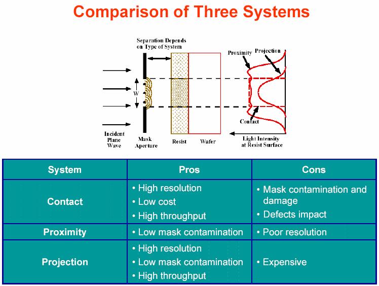
") Module 11: Photolithography Lecture 14: Photolithography 4 (Continued) 1 In the previous lecture, we have discussed the utility of the three printing modes, and their relative advantages and disadvantages.
Module 11: Photolithography Lecture 14: Photolithography 4 (Continued) 1 In the previous lecture, we have discussed the utility of the three printing modes, and their relative advantages and disadvantages.
PHGN/CHEN/MLGN 435/535: Interdisciplinary Silicon Processing Laboratory. Simple Si solar Cell!
 Where were we? Simple Si solar Cell! Two Levels of Masks - photoresist, alignment Etch and oxidation to isolate thermal oxide, deposited oxide, wet etching, dry etching, isolation schemes Doping - diffusion/ion
Oriel Flood Exposure Sources
 218 Oriel Flood Exposure Sources High intensity outputs CALIBRATION SOURCES Highly uniform, large collimated beams Efficient out of band rejection Timed exposures DEUTERIUM SOURCES ARC SOURCES INCANDESCENT
Outline. 1 Introduction. 2 Basic IC fabrication processes. 3 Fabrication techniques for MEMS. 4 Applications. 5 Mechanics issues on MEMS MDL NTHU
 Outline 1 Introduction 2 Basic IC fabrication processes 3 Fabrication techniques for MEMS 4 Applications 5 Mechanics issues on MEMS 2.2 Lithography Reading: Runyan Chap. 5, or 莊達人 Chap. 7, or Wolf and
Process Optimization
 Process Optimization Process Flow for non-critical layer optimization START Find the swing curve for the desired resist thickness. Determine the resist thickness (spin speed) from the swing curve and find
PHYS 202 OUTLINE FOR PART III LIGHT & OPTICS
 PHYS 202 OUTLINE FOR PART III LIGHT & OPTICS Electromagnetic Waves A. Electromagnetic waves S-23,24 1. speed of waves = 1/( o o ) ½ = 3 x 10 8 m/s = c 2. waves and frequency: the spectrum (a) radio red
Micro- and Nano-Technology... for Optics
 Micro- and Nano-Technology...... for Optics 3.2 Lithography U.D. Zeitner Fraunhofer Institut für Angewandte Optik und Feinmechanik Jena Printing on Stones Map of Munich Stone Print Contact Printing light
Chapter 17: Wave Optics. What is Light? The Models of Light 1/11/13
 Chapter 17: Wave Optics Key Terms Wave model Ray model Diffraction Refraction Fringe spacing Diffraction grating Thin-film interference What is Light? Light is the chameleon of the physical world. Under
Lithography Is the Designer s Brush. Lithography is indispensible for defining locations and configurations of circuit elements/functions.
 Lithography 1 Lithography Is the Designer s Brush Lithography is indispensible for defining locations and configurations of circuit elements/functions. 2 ITRS 2007 The major challenge in litho: CD, CD
Will contain image distance after raytrace Will contain image height after raytrace
 Name: LASR 51 Final Exam May 29, 2002 Answer all questions. Module numbers are for guidance, some material is from class handouts. Exam ends at 8:20 pm. Ynu Raytracing The first questions refer to the
Update on 193nm immersion exposure tool
 Update on 193nm immersion exposure tool S. Owa, H. Nagasaka, Y. Ishii Nikon Corporation O. Hirakawa and T. Yamamoto Tokyo Electron Kyushu Ltd. January 28, 2004 Litho Forum 1 What is immersion lithography?
Physics 431 Final Exam Examples (3:00-5:00 pm 12/16/2009) TIME ALLOTTED: 120 MINUTES Name: Signature:
 TIME ALLOTTED: 120 MINUTES Name: Signature:") Physics 431 Final Exam Examples (3:00-5:00 pm 12/16/2009) TIME ALLOTTED: 120 MINUTES Name: PID: Signature: CLOSED BOOK. TWO 8 1/2 X 11 SHEET OF NOTES (double sided is allowed), AND SCIENTIFIC POCKET CALCULATOR
Physics 431 Final Exam Examples (3:00-5:00 pm 12/16/2009) TIME ALLOTTED: 120 MINUTES Name: PID: Signature: CLOSED BOOK. TWO 8 1/2 X 11 SHEET OF NOTES (double sided is allowed), AND SCIENTIFIC POCKET CALCULATOR
ECEN. Spectroscopy. Lab 8. copy. constituents HOMEWORK PR. Figure. 1. Layout of. of the
 ECEN 4606 Lab 8 Spectroscopy SUMMARY: ROBLEM 1: Pedrotti 3 12-10. In this lab, you will design, build and test an optical spectrum analyzer and use it for both absorption and emission spectroscopy. The
EE 143 Microfabrication Technology Fall 2014
 EE 143 Microfabrication Technology Fall 2014 Prof. Clark T.-C. Nguyen Dept. of Electrical Engineering & Computer Sciences University of California at Berkeley Berkeley, CA 94720 EE 143: Microfabrication
The Wave Nature of Light
 The Wave Nature of Light Physics 102 Lecture 7 4 April 2002 Pick up Grating & Foil & Pin 4 Apr 2002 Physics 102 Lecture 7 1 Light acts like a wave! Last week we saw that light travels from place to place
Fiber Optic Communications
 Fiber Optic Communications ( Chapter 2: Optics Review ) presented by Prof. Kwang-Chun Ho 1 Section 2.4: Numerical Aperture Consider an optical receiver: where the diameter of photodetector surface area
Optics and Images. Lenses and Mirrors. Matthew W. Milligan
 Optics and Images Lenses and Mirrors Light: Interference and Optics I. Light as a Wave - wave basics review - electromagnetic radiation II. Diffraction and Interference - diffraction, Huygen s principle
Physics 1520, Spring 2013 Quiz 2, Form: A
 Physics 1520, Spring 2013 Quiz 2, Form: A Name: Date: Section 1. Exercises 1. The index of refraction of a certain type of glass for red light is 1.52. For violet light, it is 1.54. Which color of light,
PHY 431 Homework Set #5 Due Nov. 20 at the start of class
 PHY 431 Homework Set #5 Due Nov. 0 at the start of class 1) Newton s rings (10%) The radius of curvature of the convex surface of a plano-convex lens is 30 cm. The lens is placed with its convex side down
Key Photolithographic Outputs
 Exposure latitude Depth of Focus Exposure latitude Vs DOF plot Linearity and MEEF Isolated-Dense Bias NILS Contrast Swing Curve Reflectivity Curve 1 Exposure latitude:the range of exposure energies (usually
Optolith 2D Lithography Simulator
 2D Lithography Simulator Advanced 2D Optical Lithography Simulator 4/13/05 Introduction is a powerful non-planar 2D lithography simulator that models all aspects of modern deep sub-micron lithography It
idonus UV-LED exposure system for photolithography
 idonus UV-LED exposure system for photolithography UV-LED technology is an attractive alternative to traditional arc lamp illumination. The benefits of UV-LEDs are manyfold and significant for photolithography.
Optical Projection Printing and Modeling
 Optical Projection Printing and Modeling Overview of optical lithography, concepts, trends Basic Parameters and Effects (1-14) Resolution Depth of Focus; Proximity, MEEF, LES Image Calculation, Characterization
Purpose: Explain the top 10 phenomena and concepts. BPP-1: Resolution and Depth of Focus (1.5X)
") Basic Projection Printing (BPP) Modules Purpose: Explain the top 10 phenomena and concepts key to understanding optical projection printing BPP-1: Resolution and Depth of Focus (1.5X) BPP-2: Bragg condition
Basic Projection Printing (BPP) Modules Purpose: Explain the top 10 phenomena and concepts key to understanding optical projection printing BPP-1: Resolution and Depth of Focus (1.5X) BPP-2: Bragg condition
Computer Generated Holograms for Optical Testing
 Computer Generated Holograms for Optical Testing Dr. Jim Burge Associate Professor Optical Sciences and Astronomy University of Arizona jburge@optics.arizona.edu 520-621-8182 Computer Generated Holograms
Collimation Tester Instructions
 Description Use shear-plate collimation testers to examine and adjust the collimation of laser light, or to measure the wavefront curvature and divergence/convergence magnitude of large-radius optical
MicroSpot FOCUSING OBJECTIVES
 OFR P R E C I S I O N O P T I C A L P R O D U C T S MicroSpot FOCUSING OBJECTIVES APPLICATIONS Micromachining Microlithography Laser scribing Photoablation MAJOR FEATURES For UV excimer & high-power YAG
TECHNICAL QUICK REFERENCE GUIDE MANUFACTURING CAPABILITIES GLASS PROPERTIES COATING CURVES REFERENCE MATERIALS
 TECHNICAL QUICK REFERENCE GUIDE COATING CURVES GLASS PROPERTIES MANUFACTURING CAPABILITIES REFERENCE MATERIALS TABLE OF CONTENTS Why Edmund Optics?... 3 Anti-Reflective (AR) Coatings... 4-16 Metallic Mirror
Solid Immersion and Evanescent Wave Lithography at Numerical Apertures > 1.60
 Solid Immersion and Evanescent Wave Lithography at Numerical Apertures > 1.60 Bruce Smith Y. Fan, J. Zhou, L. Zavyalova, M. Slocum, J. Park, A. Bourov, E. Piscani, N. Lafferty, A. Estroff Rochester Institute
The Formation of an Aerial Image, part 3
 T h e L i t h o g r a p h y T u t o r (July 1993) The Formation of an Aerial Image, part 3 Chris A. Mack, FINLE Technologies, Austin, Texas In the last two issues, we described how a projection system
Micro- and Nano-Technology... for Optics
 Micro- and Nano-Technology...... for Optics 3.2 Lithography U.D. Zeitner Fraunhofer Institut für Angewandte Optik und Feinmechanik Jena Printing on Stones Map of Munich Stone Print Shadow Printing Photomask
Exercise 8: Interference and diffraction
 Physics 223 Name: Exercise 8: Interference and diffraction 1. In a two-slit Young s interference experiment, the aperture (the mask with the two slits) to screen distance is 2.0 m, and a red light of wavelength
Diffraction. Interference with more than 2 beams. Diffraction gratings. Diffraction by an aperture. Diffraction of a laser beam
 Diffraction Interference with more than 2 beams 3, 4, 5 beams Large number of beams Diffraction gratings Equation Uses Diffraction by an aperture Huygen s principle again, Fresnel zones, Arago s spot Qualitative
OPTICAL PRINCIPLES OF MICROSCOPY. Interuniversity Course 28 December 2003 Aryeh M. Weiss Bar Ilan University
 OPTICAL PRINCIPLES OF MICROSCOPY Interuniversity Course 28 December 2003 Aryeh M. Weiss Bar Ilan University FOREWORD This slide set was originally presented at the ISM Workshop on Theoretical and Experimental
Lecture 8. Microlithography
 Lecture 8 Microlithography Lithography Introduction Process Flow Wafer Exposure Systems Masks Resists State of the Art Lithography Next Generation Lithography (NGL) Recommended videos: http://www.youtube.com/user/asmlcompany#p/search/1/jh6urfqt_d4
CHAPTER 2 Principle and Design
 CHAPTER 2 Principle and Design The binary and gray-scale microlens will be designed and fabricated. Silicon nitride and photoresist will be taken as the material of the microlens in this thesis. The design
Optical Components for Laser Applications. Günter Toesko - Laserseminar BLZ im Dezember
 Günter Toesko - Laserseminar BLZ im Dezember 2009 1 Aberrations An optical aberration is a distortion in the image formed by an optical system compared to the original. It can arise for a number of reasons
EE119 Introduction to Optical Engineering Spring 2003 Final Exam. Name:
 EE119 Introduction to Optical Engineering Spring 2003 Final Exam Name: SID: CLOSED BOOK. THREE 8 1/2 X 11 SHEETS OF NOTES, AND SCIENTIFIC POCKET CALCULATOR PERMITTED. TIME ALLOTTED: 180 MINUTES Fundamental
Microlithography. exposing radiation. mask. imaging system (low pass filter) photoresist. develop. etch
 photoresist. develop. etch") Microlithography Geometry Trends Master Patterns: Mask technology Pattern Transfer: Mask Aligner technology Wafer Transfer Media: Photo resist technology mask blank: transparent, mechanically rigid masking
Microlithography Geometry Trends Master Patterns: Mask technology Pattern Transfer: Mask Aligner technology Wafer Transfer Media: Photo resist technology mask blank: transparent, mechanically rigid masking
High-resolution microlithography using a 193nm excimer laser source. Nadeem H. Rizvi, Dominic Ashworth, Julian S. Cashmore and Malcolm C.
 High-resolution microlithography using a 193nm excimer laser source. Nadeem H. Rizvi, Dominic Ashworth, Julian S. Cashmore and Malcolm C. Gower Exitech Limited Hanborough Park, Long Hanborough, Oxford
Project Staff: Timothy A. Savas, Michael E. Walsh, Thomas B. O'Reilly, Dr. Mark L. Schattenburg, and Professor Henry I. Smith
 9. Interference Lithography Sponsors: National Science Foundation, DMR-0210321; Dupont Agreement 12/10/99 Project Staff: Timothy A. Savas, Michael E. Walsh, Thomas B. O'Reilly, Dr. Mark L. Schattenburg,
Chapter Ray and Wave Optics
 109 Chapter Ray and Wave Optics 1. An astronomical telescope has a large aperture to [2002] reduce spherical aberration have high resolution increase span of observation have low dispersion. 2. If two
Dr. Dirk Meyners Prof. Wagner. Wagner / Meyners Micro / Nanosystems Technology
 Micro/Nanosystems Technology Dr. Dirk Meyners Prof. Wagner 1 Outline - Lithography Overview - UV-Lithography - Resolution Enhancement Techniques - Electron Beam Lithography - Patterning with Focused Ion
microscopy A great online resource Molecular Expressions, a Microscope Primer Partha Roy
 Fundamentals of optical microscopy A great online resource Molecular Expressions, a Microscope Primer http://micro.magnet.fsu.edu/primer/index.html Partha Roy 1 Why microscopy Topics Functions of a microscope
CHAPTER 7. Components of Optical Instruments
 CHAPTER 7 Components of Optical Instruments From: Principles of Instrumental Analysis, 6 th Edition, Holler, Skoog and Crouch. CMY 383 Dr Tim Laurens NB Optical in this case refers not only to the visible
Optical Coherence: Recreation of the Experiment of Thompson and Wolf
 Optical Coherence: Recreation of the Experiment of Thompson and Wolf David Collins Senior project Department of Physics, California Polytechnic State University San Luis Obispo June 2010 Abstract The purpose
Test procedures Page: 1 of 5
 Test procedures Page: 1 of 5 1 Scope This part of document establishes uniform requirements for measuring the numerical aperture of optical fibre, thereby assisting in the inspection of fibres and cables
Radial Coupling Method for Orthogonal Concentration within Planar Micro-Optic Solar Collectors
 Radial Coupling Method for Orthogonal Concentration within Planar Micro-Optic Solar Collectors Jason H. Karp, Eric J. Tremblay and Joseph E. Ford Photonics Systems Integration Lab University of California
NANOFABRICATION, THE NEW GENERATION OF LITHOGRAPHY. Cheng-Sheng Huang & Alvin Chang ABSTRACT
 NANOFABRICATION, THE NEW GENERATION OF LITHOGRAPHY Cheng-Sheng Huang & Alvin Chang ABSTRACT Fabrication on the micro- and nano-structure has opened the new horizons in science and engineering. The success
UV LED ILLUMINATION STEPPER OFFERS HIGH PERFORMANCE AND LOW COST OF OWNERSHIP
 UV LED ILLUMINATION STEPPER OFFERS HIGH PERFORMANCE AND LOW COST OF OWNERSHIP Casey Donaher, Rudolph Technologies Herbert J. Thompson, Rudolph Technologies Chin Tiong Sim, Rudolph Technologies Rudolph
Amphibian XIS: An Immersion Lithography Microstepper Platform
 Amphibian XIS: An Immersion Lithography Microstepper Platform Bruce W. Smith, Anatoly Bourov, Yongfa Fan, Frank Cropanese, Peter Hammond Rochester Institute of Technology, Microelectronic Engineering Department,
Photolithography Module
 Electronics Workforce Development System Photolithography Module Introduction Photolithography Module This module will teach students the different types of microlithographic systems being used today,
Compact High Intensity Light Source
 Compact High Intensity Light Source General When a broadband light source in the ultraviolet-visible-near infrared portion of the spectrum is required, an arc lamp has no peer. The intensity of an arc
k λ NA Resolution of optical systems depends on the wavelength visible light λ = 500 nm Extreme ultra-violet and soft x-ray light λ = 1-50 nm
 Resolution of optical systems depends on the wavelength visible light λ = 500 nm Spatial Resolution = k λ NA EUV and SXR microscopy can potentially resolve full-field images with 10-100x smaller features
Photonics and Optical Communication
 Photonics and Optical Communication (Course Number 300352) Spring 2007 Dr. Dietmar Knipp Assistant Professor of Electrical Engineering http://www.faculty.iu-bremen.de/dknipp/ 1 Photonics and Optical Communication
EUV Plasma Source with IR Power Recycling
 1 EUV Plasma Source with IR Power Recycling Kenneth C. Johnson kjinnovation@earthlink.net 1/6/2016 (first revision) Abstract Laser power requirements for an EUV laser-produced plasma source can be reduced
Applications of Optics
 Nicholas J. Giordano www.cengage.com/physics/giordano Chapter 26 Applications of Optics Marilyn Akins, PhD Broome Community College Applications of Optics Many devices are based on the principles of optics
immersion optics Immersion Lithography with ASML HydroLith TWINSCAN System Modifications for Immersion Lithography by Bob Streefkerk
 immersion optics Immersion Lithography with ASML HydroLith by Bob Streefkerk For more than 25 years, many in the semiconductor industry have predicted the end of optical lithography. Recent developments,
Excimer laser projector for microelectronics applications
 Excimer laser projector for microelectronics applications P T Rumsby and M C Gower Exitech Ltd Hanborough Park, Long Hanborough, Oxford OX8 8LH, England ABSTRACT Fully integrated excimer laser mask macro
Refractive Power of a Surface. Exposure Sources. Thin Lenses. Thick Lenses. High Pressure Hg Arc Lamp Spectrum
 eractive Power o a Surace The reractive power P is measured in diopters when the radius is expressed in meters. n and n are the reractive indices o the two media. EE-57: icrofabrication n n P n n Exposure
Bandpass Interference Filters
 Precise control of center wavelength and bandpass shape Wide selection of stock wavelengths from 250 nm-1550 nm Selection of bandwidths Available in 1/2 and 1 sizes High peak transmission values Excellent
High Performance Thin Film Optical Coatings Technical Reference Document 09/13. Coatings Capabilities. Heat Control - Hot Mirror Filters
 Heat Control - Hot Mirror Filters A hot mirror is in essence a thin film coating applied to substrates in an effort to reflect infra-red radiation either as a means to harness the reflected wavelengths
TSBB09 Image Sensors 2018-HT2. Image Formation Part 1
 TSBB09 Image Sensors 2018-HT2 Image Formation Part 1 Basic physics Electromagnetic radiation consists of electromagnetic waves With energy That propagate through space The waves consist of transversal
Guide to SPEX Optical Spectrometer
 Guide to SPEX Optical Spectrometer GENERAL DESCRIPTION A spectrometer is a device for analyzing an input light beam into its constituent wavelengths. The SPEX model 1704 spectrometer covers a range from
Point Spread Function. Confocal Laser Scanning Microscopy. Confocal Aperture. Optical aberrations. Alternative Scanning Microscopy
 Bi177 Lecture 5 Adding the Third Dimension Wide-field Imaging Point Spread Function Deconvolution Confocal Laser Scanning Microscopy Confocal Aperture Optical aberrations Alternative Scanning Microscopy
Experimental Physics. Experiment C & D: Pulsed Laser & Dye Laser. Course: FY12. Project: The Pulsed Laser. Done by: Wael Al-Assadi & Irvin Mangwiza
 Experiment C & D: Course: FY1 The Pulsed Laser Done by: Wael Al-Assadi Mangwiza 8/1/ Wael Al Assadi Mangwiza Experiment C & D : Introduction: Course: FY1 Rev. 35. Page: of 16 1// In this experiment we
Applied Optics. , Physics Department (Room #36-401) , ,
 , ,") Applied Optics Professor, Physics Department (Room #36-401) 2290-0923, 019-539-0923, shsong@hanyang.ac.kr Office Hours Mondays 15:00-16:30, Wednesdays 15:00-16:30 TA (Ph.D. student, Room #36-415) 2290-0921,
Applied Optics Professor, Physics Department (Room #36-401) 2290-0923, 019-539-0923, shsong@hanyang.ac.kr Office Hours Mondays 15:00-16:30, Wednesdays 15:00-16:30 TA (Ph.D. student, Room #36-415) 2290-0921,
Bandpass Edge Dichroic Notch & More
 Edmund Optics BROCHURE Filters COPYRIGHT 217 EDMUND OPTICS, INC. ALL RIGHTS RESERVED 1/17 Bandpass Edge Dichroic Notch & More Contact us for a Stock or Custom Quote Today! USA: +1-856-547-3488 EUROPE:
Integrated Focusing Photoresist Microlenses on AlGaAs Top-Emitting VCSELs
 Integrated Focusing Photoresist Microlenses on AlGaAs Top-Emitting VCSELs Andrea Kroner We present 85 nm wavelength top-emitting vertical-cavity surface-emitting lasers (VCSELs) with integrated photoresist
Absentee layer. A layer of dielectric material, transparent in the transmission region of
 Glossary of Terms A Absentee layer. A layer of dielectric material, transparent in the transmission region of the filter, due to a phase thickness of 180. Absorption curve, absorption spectrum. The relative