Photolithography 光刻 Part I: Optics
|
|
|
- Edward Gray
- 5 years ago
- Views:
Transcription


1 微纳光电子材料与器件工艺原理 Photolithography 光刻 Part I: Optics Xing Sheng 盛兴 Department of Electronic Engineering Tsinghua University 1

2 Integrate Circuits Moore's law transistor number transistor size 5


3 Transistor size s 1 cm ~ 2 mm < 100 nm revolution evolution 6

4 CMOS Process 'Lithography is the cornerstone of modern IC technology' ---- Silicon VLSI, Plummer et al., 7

5 Lithography litho- 石头 -graph 图案 8

6 Photography 曝光 显影 打印 9
7 Photolithography( 光刻 ) Xing Sheng, EE@Tsinghua 10
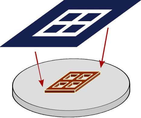
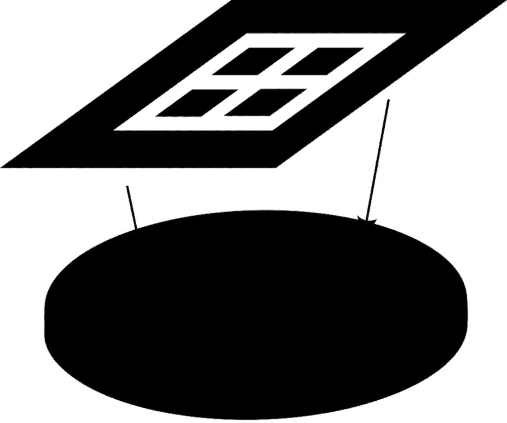
 Video 光刻胶 光源 掩膜 11")
8 Photolithography( 光刻 ) Video 光刻胶 光源 掩膜 11
 接触式接近式投影式")
9 Exposure ( 曝光 ) 接触式接近式投影式 12

10 Exposure ( 曝光 ) stepper ( 步进投影 ) Video mass chip production in industry 13
11 Resolution ideal case actual case 14
12 Resolution the smaller, the harder 15

13 Resolution diffraction: light is a wave! 16
14 Resolution contact and proximity mode R resolution wavelength g gap size R ~ g smaller, g ---> smaller R UV, DUV, EUV, x-ray,... g minimum: resist film thickness 17

15 projection mode Resolution 18
16 Resolution ideal MTF = 1 poor MTF ~ 0 MTF =? modulation transfer function (MTF) MTF I I max max I I min min 19
")
17 Resolution diffraction pattern (Airy's disk) 20
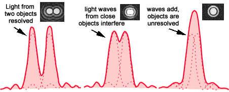
18 Resolution 21
19 Resolution resolution smaller, larger NA ---> smaller resolution UV, DUV, EUV, x-ray,... n refractive index (air: 1, oil: 1.4~1.7) sin maximum =

20 Depth of Focus (DOF) Xing Sheng, off focus on focus off focus trade-off between resolution and DOF 23

21 Depth of Focus (DOF) Xing Sheng, 24

22 Spatial Coherence 25
23 Resolution Improvement Xing Sheng, R ~ nsin reduce increase n??? 26

24 Immersion Lithography Xing Sheng, R ~ nsin n > 1.0 n = 1.0 high index fluid n = 1.7 resolution is reduced by ~40% 27
25 Phase Shift Mask 28
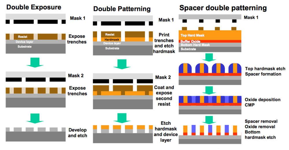
26 Double Patterning 29
 mask")
27 Optical Proximity Correction (OPC) mask resist 30
28 Photomasks ( 掩膜 ) 31


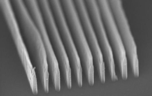
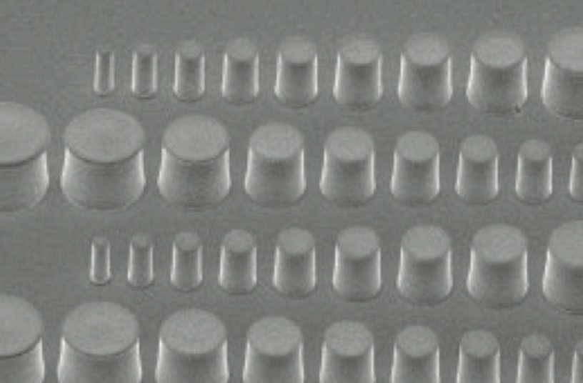
29 Photomasks ( 掩膜 ) Layout design CAD tools see examples Example Transparency film flexible mask design layout Chrome mask glass substrate chrome coating transparency film chrome mask 32

30 Photomasks ( 掩膜 ) write by laser or Ebeam 33

31 Mercury (Hg) arc lamp Light Sources g-line 436 nm, h-line 405 nm, i-line 365 nm R ~ nsin 34


32 Light Sources Mercury (Hg) arc lamp g-line 436 nm, h-line 405 nm, i-line 365 nm yellow light in cleanroom 35
 X-ray Tin (Sn) plasma lasers, 13.5 nm 0.01 ~ 10 nm Electron beam (E-beam)... 36")
33 Light Sources Deep UV (DUV) excimer lasers, KrF (248 nm), ArF (193 nm) R ~ nsin Extreme UV (EUV) X-ray Tin (Sn) plasma lasers, 13.5 nm 0.01 ~ 10 nm Electron beam (E-beam)... 36
34 Optics for EUV quartz glass metals air at EUV: glass is not transparent metal is not reflective even air is absorptive 37


35 Optics for EUV multilayer mirrors (Mo/Si) reflective masks 38
 EUV (13.")
36 Optics optical loss > 95% UV (365 nm) EUV (13.5 nm) 39

 resolution ~ 10 nm")
37 Equipment UV (365 nm) resolution ~ 2 m price ~ 200,000 RMB EUV (13.5 nm) resolution ~ 10 nm price ~ 100,000,000 $$$ 40

38 wavelength 0.1~10 nm X-ray Lithography 41
 proximity")
39 Electron Beam (Ebeam) Lithography similar to a scanning electron microscope (SEM) proximity effect 42
40 Wavelength example: for V = 30 kv, = nm The resolution is limited by secondary electrons resolution ~ 10 nm No mask for electron, only direct writing! Xing Sheng, EE@Tsinghua Electron Beam (Ebeam) Lithography ( nm) 1.23 "To cover the 700 cm 2 surface area of a 300 mm silicon wafer, the minimum write time would extend to 7*10 8 seconds, about 22 years." - Wikipedia Only for research purposes now V 43
41 NanoPhotonics 44


42 Optical Cloak J. Valentine, et al., Nature Mater. 8, 568 (2008) 45

43 Metalens 40 m 300 nm M. Khorasaninejad, et al., Science 352, 1190 (2016) 46
44 Thank you for your attention 48
Lithography. 3 rd. lecture: introduction. Prof. Yosi Shacham-Diamand. Fall 2004
 Lithography 3 rd lecture: introduction Prof. Yosi Shacham-Diamand Fall 2004 1 List of content Fundamental principles Characteristics parameters Exposure systems 2 Fundamental principles Aerial Image Exposure
Part 5-1: Lithography
 Part 5-1: Lithography Yao-Joe Yang 1 Pattern Transfer (Patterning) Types of lithography systems: Optical X-ray electron beam writer (non-traditional, no masks) Two-dimensional pattern transfer: limited
Section 2: Lithography. Jaeger Chapter 2 Litho Reader. The lithographic process
 Section 2: Lithography Jaeger Chapter 2 Litho Reader The lithographic process Photolithographic Process (a) (b) (c) (d) (e) (f) (g) Substrate covered with silicon dioxide barrier layer Positive photoresist
Section 2: Lithography. Jaeger Chapter 2 Litho Reader. EE143 Ali Javey Slide 5-1
 Section 2: Lithography Jaeger Chapter 2 Litho Reader EE143 Ali Javey Slide 5-1 The lithographic process EE143 Ali Javey Slide 5-2 Photolithographic Process (a) (b) (c) (d) (e) (f) (g) Substrate covered
Section 2: Lithography. Jaeger Chapter 2. EE143 Ali Javey Slide 5-1
 Section 2: Lithography Jaeger Chapter 2 EE143 Ali Javey Slide 5-1 The lithographic process EE143 Ali Javey Slide 5-2 Photolithographic Process (a) (b) (c) (d) (e) (f) (g) Substrate covered with silicon
Lecture 5. Optical Lithography
 Lecture 5 Optical Lithography Intro For most of microfabrication purposes the process (e.g. additive, subtractive or implantation) has to be applied selectively to particular areas of the wafer: patterning
EE143 Fall 2016 Microfabrication Technologies. Lecture 3: Lithography Reading: Jaeger, Chap. 2
 EE143 Fall 2016 Microfabrication Technologies Lecture 3: Lithography Reading: Jaeger, Chap. 2 Prof. Ming C. Wu wu@eecs.berkeley.edu 511 Sutardja Dai Hall (SDH) 1-1 The lithographic process 1-2 1 Photolithographic
Photolithography I ( Part 1 )
") 1 Photolithography I ( Part 1 ) Chapter 13 : Semiconductor Manufacturing Technology by M. Quirk & J. Serda Bjørn-Ove Fimland, Department of Electronics and Telecommunication, Norwegian University of Science
1 Photolithography I ( Part 1 ) Chapter 13 : Semiconductor Manufacturing Technology by M. Quirk & J. Serda Bjørn-Ove Fimland, Department of Electronics and Telecommunication, Norwegian University of Science
5. Lithography. 1. photolithography intro: overall, clean room 2. principle 3. tools 4. pattern transfer 5. resolution 6. next-gen
 5. Lithography 1. photolithography intro: overall, clean room 2. principle 3. tools 4. pattern transfer 5. resolution 6. next-gen References: Semiconductor Devices: Physics and Technology. 2 nd Ed. SM
MICROCHIP MANUFACTURING by S. Wolf
 MICROCHIP MANUFACTURING by S. Wolf Chapter 19 LITHOGRAPHY II: IMAGE-FORMATION and OPTICAL HARDWARE 2004 by LATTICE PRESS CHAPTER 19 - CONTENTS Preliminaries: Wave- Motion & The Behavior of Light Resolution
Photolithography II ( Part 2 )
") 1 Photolithography II ( Part 2 ) Chapter 14 : Semiconductor Manufacturing Technology by M. Quirk & J. Serda Saroj Kumar Patra, Department of Electronics and Telecommunication, Norwegian University of Science
1 Photolithography II ( Part 2 ) Chapter 14 : Semiconductor Manufacturing Technology by M. Quirk & J. Serda Saroj Kumar Patra, Department of Electronics and Telecommunication, Norwegian University of Science
Optical Lithography. Keeho Kim Nano Team / R&D DongbuAnam Semi
 Optical Lithography Keeho Kim Nano Team / R&D DongbuAnam Semi Contents Lithography = Photolithography = Optical Lithography CD : Critical Dimension Resist Pattern after Development Exposure Contents Optical
ECSE 6300 IC Fabrication Laboratory Lecture 3 Photolithography. Lecture Outline
 ECSE 6300 IC Fabrication Laboratory Lecture 3 Photolithography Prof. James J. Q. Lu Bldg. CII, Rooms 6229 Rensselaer Polytechnic Institute Troy, NY 12180 Tel. (518)276 2909 e mails: luj@rpi.edu http://www.ecse.rpi.edu/courses/s18/ecse
EE-527: MicroFabrication
 EE-57: MicroFabrication Exposure and Imaging Photons white light Hg arc lamp filtered Hg arc lamp excimer laser x-rays from synchrotron Electrons Ions Exposure Sources focused electron beam direct write
MICRO AND NANOPROCESSING TECHNOLOGIES
 MICRO AND NANOPROCESSING TECHNOLOGIES LECTURE 4 Optical lithography Concepts and processes Lithography systems Fundamental limitations and other issues Photoresists Photolithography process Process parameter
Lecture 8. Microlithography
 Lecture 8 Microlithography Lithography Introduction Process Flow Wafer Exposure Systems Masks Resists State of the Art Lithography Next Generation Lithography (NGL) Recommended videos: http://www.youtube.com/user/asmlcompany#p/search/1/jh6urfqt_d4
EE 143 Microfabrication Technology Fall 2014
 EE 143 Microfabrication Technology Fall 2014 Prof. Clark T.-C. Nguyen Dept. of Electrical Engineering & Computer Sciences University of California at Berkeley Berkeley, CA 94720 EE 143: Microfabrication
Process Optimization
 Process Optimization Process Flow for non-critical layer optimization START Find the swing curve for the desired resist thickness. Determine the resist thickness (spin speed) from the swing curve and find
Lecture 7. Lithography and Pattern Transfer. Reading: Chapter 7
 Lecture 7 Lithography and Pattern Transfer Reading: Chapter 7 Used for Pattern transfer into oxides, metals, semiconductors. 3 types of Photoresists (PR): Lithography and Photoresists 1.) Positive: PR
T in sec, I in W/cm 2, E in J/cm 2
 Exposures from Mask Aligner into Resist Mask aligner images created by shadowing from mask into resist Soft contact and Proximity good for 3 micron structures Vacuum Hard Contact: no shadow effects at
Photolithography Module
 Electronics Workforce Development System Photolithography Module Introduction Photolithography Module This module will teach students the different types of microlithographic systems being used today,
Semiconductor Manufacturing Technology. Semiconductor Manufacturing Technology. Photolithography: Resist Development and Advanced Lithography
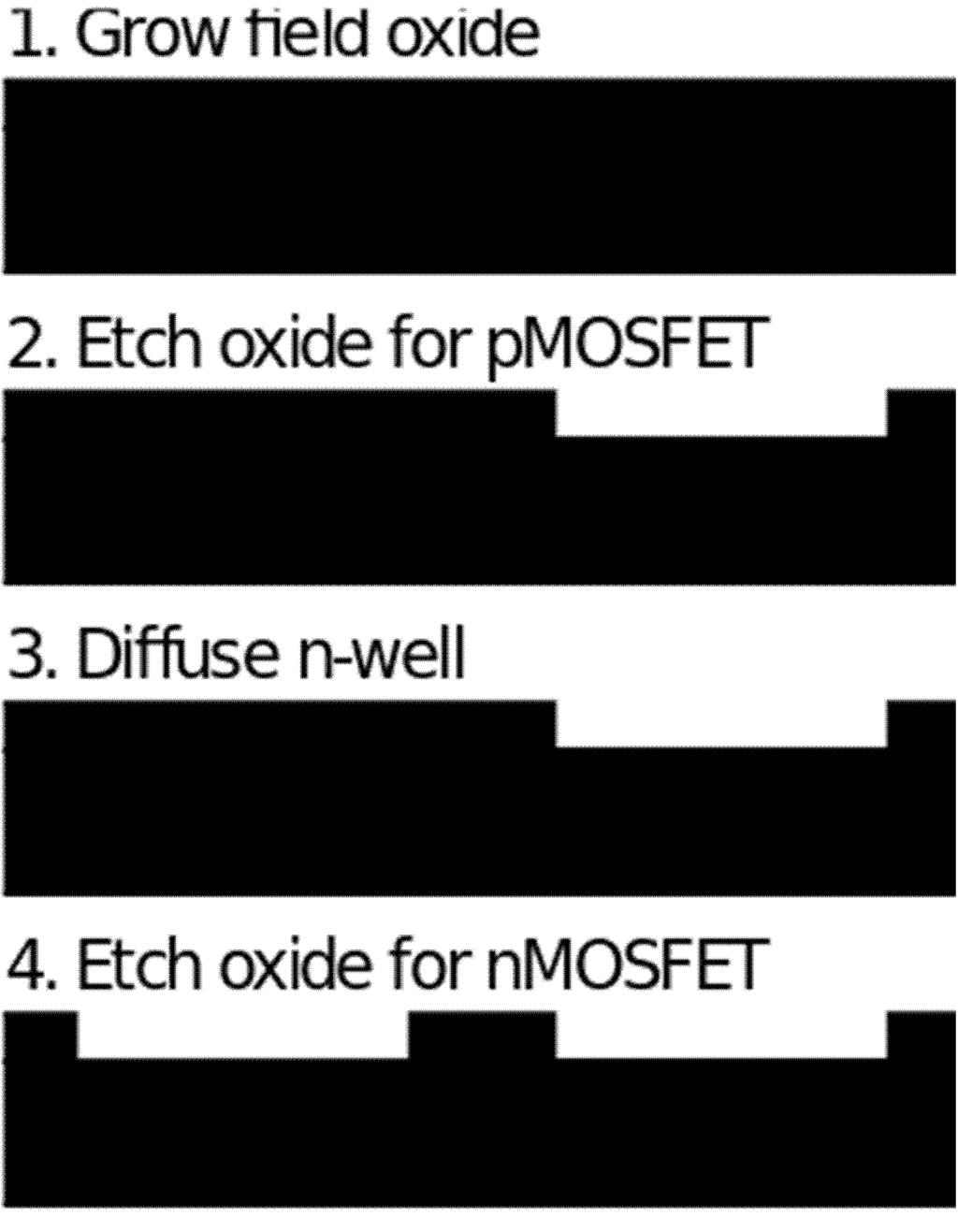
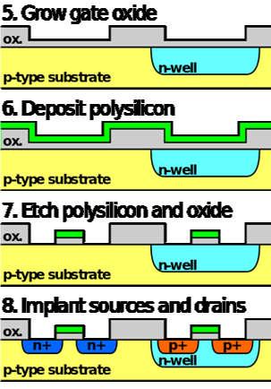
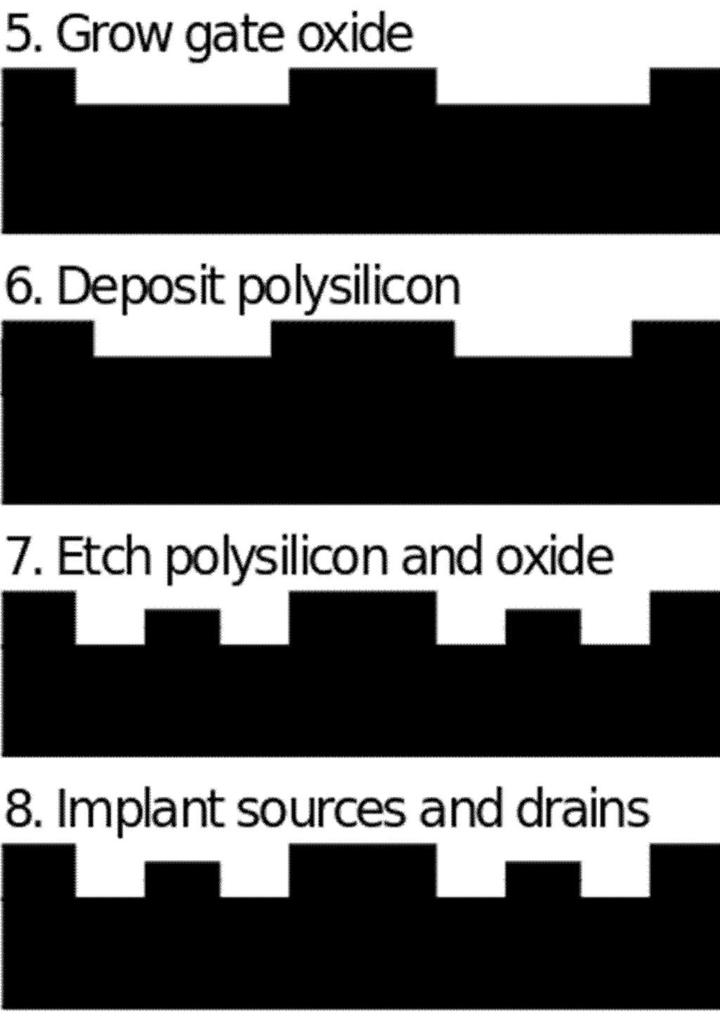
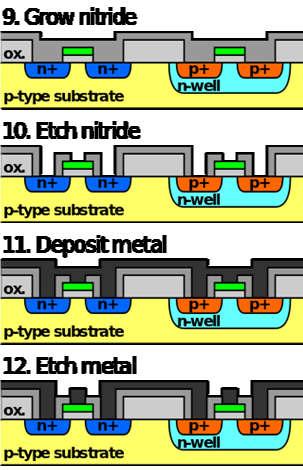
 Semiconductor Manufacturing Technology Michael Quirk & Julian Serda October 2001 by Prentice Hall Chapter 15 Photolithography: Resist Development and Advanced Lithography Eight Basic Steps of Photolithography
Nanotechnology I+II 2006 / 07
 Nanotechnology for engineers Winter semester 2006-2007 Nanotechnology I+II 2006 / 07 Juergen Brugger & Patrik Hoffmann & Teams Course agenda (winter semester) Nanotechnology I winter semester (23.10.06-9.2.06)
Photolithography Technology and Application
 Photolithography Technology and Application Jeff Tsai Director, Graduate Institute of Electro-Optical Engineering Tatung University Art or Science? Lind width = 100 to 5 micron meter!! Resolution = ~ 3
Optical Issues in Photolithography
 OpenStax-CNX module: m25448 1 Optical Issues in Photolithography Andrew R. Barron This work is produced by OpenStax-CNX and licensed under the Creative Commons Attribution License 3.0 note: This module
NANOFABRICATION, THE NEW GENERATION OF LITHOGRAPHY. Cheng-Sheng Huang & Alvin Chang ABSTRACT
 NANOFABRICATION, THE NEW GENERATION OF LITHOGRAPHY Cheng-Sheng Huang & Alvin Chang ABSTRACT Fabrication on the micro- and nano-structure has opened the new horizons in science and engineering. The success
Photolithography. References: Introduction to Microlithography Thompson, Willson & Bowder, 1994
 Photolithography References: Introduction to Microlithography Thompson, Willson & Bowder, 1994 Microlithography, Science and Technology Sheats & Smith, 1998 Any other Microlithography or Photolithography
Module - 2 Lecture - 13 Lithography I
 Nano Structured Materials-Synthesis, Properties, Self Assembly and Applications Prof. Ashok. K.Ganguli Department of Chemistry Indian Institute of Technology, Delhi Module - 2 Lecture - 13 Lithography
Lithography. Development of High-Quality Attenuated Phase-Shift Masks
 Lithography S P E C I A L Development of High-Quality Attenuated Phase-Shift Masks by Toshihiro Ii and Masao Otaki, Toppan Printing Co., Ltd. Along with the year-by-year acceleration of semiconductor device
Chapter 6. Photolithography
 Chapter 6 Photolithography 2006/4/10 1 Objectives List the four components of the photoresist Describe the difference between +PR and PR Describe a photolithography process sequence List four alignment
T in sec, I in W/cm 2, E in J/cm 2
 Exposures from Mask Aligner into Resist Mask aligner images created by shadowing from mask into resist Soft contact and Proximity good for 3 micron structures Vacuum Hard Contact: no shadow effects at
Major Fabrication Steps in MOS Process Flow
 Major Fabrication Steps in MOS Process Flow UV light Mask oxygen Silicon dioxide photoresist exposed photoresist oxide Silicon substrate Oxidation (Field oxide) Photoresist Coating Mask-Wafer Alignment
Device Fabrication: Photolithography
 Device Fabrication: Photolithography 1 Objectives List the four components of the photoresist Describe the difference between +PR and PR Describe a photolithography process sequence List four alignment
Lecture 13 Basic Photolithography
 Lecture 13 Basic Photolithography Chapter 12 Wolf and Tauber 1/64 Announcements Homework: Homework 3 is due today, please hand them in at the front. Will be returned one week from Thursday (16 th Nov).
Micro- and Nano-Technology... for Optics
 Micro- and Nano-Technology...... for Optics 3.2 Lithography U.D. Zeitner Fraunhofer Institut für Angewandte Optik und Feinmechanik Jena Printing on Stones Map of Munich Stone Print Shadow Printing Photomask
Newer process technology (since 1999) includes :
 includes :") Newer process technology (since 1999) includes : copper metalization hi-k dielectrics for gate insulators si on insulator strained silicon lo-k dielectrics for interconnects Immersion lithography for masks
Newer process technology (since 1999) includes : copper metalization hi-k dielectrics for gate insulators si on insulator strained silicon lo-k dielectrics for interconnects Immersion lithography for masks
PHGN/CHEN/MLGN 435/535: Interdisciplinary Silicon Processing Laboratory. Simple Si solar Cell!
 Where were we? Simple Si solar Cell! Two Levels of Masks - photoresist, alignment Etch and oxidation to isolate thermal oxide, deposited oxide, wet etching, dry etching, isolation schemes Doping - diffusion/ion
Exercise 8: Interference and diffraction
 Physics 223 Name: Exercise 8: Interference and diffraction 1. In a two-slit Young s interference experiment, the aperture (the mask with the two slits) to screen distance is 2.0 m, and a red light of wavelength
State-of-the-art device fabrication techniques
 State-of-the-art device fabrication techniques! Standard Photo-lithography and e-beam lithography! Advanced lithography techniques used in semiconductor industry Deposition: Thermal evaporation, e-gun
Module 11: Photolithography. Lecture 14: Photolithography 4 (Continued)
") Module 11: Photolithography Lecture 14: Photolithography 4 (Continued) 1 In the previous lecture, we have discussed the utility of the three printing modes, and their relative advantages and disadvantages.
Module 11: Photolithography Lecture 14: Photolithography 4 (Continued) 1 In the previous lecture, we have discussed the utility of the three printing modes, and their relative advantages and disadvantages.
Intel's 65 nm Logic Technology Demonstrated on 0.57 µm 2 SRAM Cells
 Intel's 65 nm Logic Technology Demonstrated on 0.57 µm 2 SRAM Cells Mark Bohr Intel Senior Fellow Director of Process Architecture & Integration Intel 1 What are We Announcing? Intel has fabricated fully-functional
Clean Room Technology Optical Lithography. Lithography I. takenfrombdhuey
 Clean Room Technology Optical Lithography Lithography I If the automobile had followed the same development cycle as the computer, a Rolls Royce would today cost $100, get a million miles per gallon, and
T in sec, I in W/cm 2, E in J/cm 2
 Exposures from Mask Aligner into Resist Mask aligner images created by shadowing from mask into resist Soft contact and Proximity good for 3 micron structures Vacuum Hard Contact: no shadow effects at
Institute of Solid State Physics. Technische Universität Graz. Lithography. Peter Hadley
 Technische Universität Graz Institute of Solid State Physics Lithography Peter Hadley http://www.cleanroom.byu.edu/virtual_cleanroom.parts/lithography.html http://www.cleanroom.byu.edu/su8.phtml Spin coater
Microlithography. exposing radiation. mask. imaging system (low pass filter) photoresist. develop. etch
 photoresist. develop. etch") Microlithography Geometry Trends Master Patterns: Mask technology Pattern Transfer: Mask Aligner technology Wafer Transfer Media: Photo resist technology mask blank: transparent, mechanically rigid masking
Microlithography Geometry Trends Master Patterns: Mask technology Pattern Transfer: Mask Aligner technology Wafer Transfer Media: Photo resist technology mask blank: transparent, mechanically rigid masking
Micro- and Nano-Technology... for Optics
 Micro- and Nano-Technology...... for Optics 3.2 Lithography U.D. Zeitner Fraunhofer Institut für Angewandte Optik und Feinmechanik Jena Printing on Stones Map of Munich Stone Print Contact Printing light
Innovative Mask Aligner Lithography for MEMS and Packaging
 Innovative Mask Aligner Lithography for MEMS and Packaging Dr. Reinhard Voelkel CEO SUSS MicroOptics SA September 9 th, 2010 1 SUSS Micro-Optics SUSS MicroOptics is a leading supplier for high-quality
THE CHARACTERIZATION OF CHROMELESS PHASE SHIFT MASK TECHNIQUE FOR SUB-45NM LITHOGRAPHY TAN SOON YOENG
 THE CHARACTERIZATION OF CHROMELESS PHASE SHIFT MASK TECHNIQUE FOR SUB-45NM LITHOGRAPHY TAN SOON YOENG NATIONAL UNIVERSITY OF SINGAPORE 2008 THE CHARACTERIZATION OF CHROMELESS PHASE SHIFT MASK TECHNIQUE
Advanced Digital Integrated Circuits. Lecture 2: Scaling Trends. Announcements. No office hour next Monday. Extra office hour Tuesday 2-3pm
 EE241 - Spring 20 Advanced Digital Integrated Circuits Lecture 2: Scaling Trends and Features of Modern Technologies Announcements No office hour next Monday Extra office hour Tuesday 2-3pm 2 1 Outline
Supplementary Information for: Immersion Meta-lenses at Visible Wavelengths for Nanoscale Imaging
 Supplementary Information for: Immersion Meta-lenses at Visible Wavelengths for Nanoscale Imaging Wei Ting Chen 1,, Alexander Y. Zhu 1,, Mohammadreza Khorasaninejad 1, Zhujun Shi 2, Vyshakh Sanjeev 1,3
Optical Lithography. Here Is Why. Burn J. Lin SPIE PRESS. Bellingham, Washington USA
 Optical Lithography Here Is Why Burn J. Lin SPIE PRESS Bellingham, Washington USA Contents Preface xiii Chapter 1 Introducing Optical Lithography /1 1.1 The Role of Lithography in Integrated Circuit Fabrication
Optical Projection Printing and Modeling
 Optical Projection Printing and Modeling Overview of optical lithography, concepts, trends Basic Parameters and Effects (1-14) Resolution Depth of Focus; Proximity, MEEF, LES Image Calculation, Characterization
Mask Technology Development in Extreme-Ultraviolet Lithography
 Mask Technology Development in Extreme-Ultraviolet Lithography Anthony Yen September 6, 2013 Projected End of Optical Lithography 2013 TSMC, Ltd 1976 1979 1982 1985 1988 1991 1994 1997 2000 2003 2007 2012
Discovering Electrical & Computer Engineering. Carmen S. Menoni Professor Week 3 armain.
 Discovering Electrical & Computer Engineering Carmen S. Menoni Professor Week 3 http://www.engr.colostate.edu/ece103/semin armain.html TOP TECH 2012 SPECIAL REPORT IEEE SPECTRUM PAGE 28, JANUARY 2012 P.E.
Optical Requirements
 Optical Requirements Transmission vs. Film Thickness A pellicle needs a good light transmission and long term transmission stability. Transmission depends on the film thickness, film material and any anti-reflective
Solid Immersion and Evanescent Wave Lithography at Numerical Apertures > 1.60
 Solid Immersion and Evanescent Wave Lithography at Numerical Apertures > 1.60 Bruce Smith Y. Fan, J. Zhou, L. Zavyalova, M. Slocum, J. Park, A. Bourov, E. Piscani, N. Lafferty, A. Estroff Rochester Institute
Chapter 6 Photolithography
 Chapter 6 Photolithography Hong Xiao, Ph. D. hxiao89@hotmail.com www2.austin.cc.tx.us/hongxiao/book.htm Hong Xiao, Ph. D. www2.austin.cc.tx.us/hongxiao/book.htm 1 Objectives List the four components of
Optical Microlithography XXVIII
 PROCEEDINGS OF SPIE Optical Microlithography XXVIII Kafai Lai Andreas Erdmann Editors 24-26 February 2015 San Jose, California, United States Sponsored by SPIE Cosponsored by Cymer, an ASML company (United
Outline. 1 Introduction. 2 Basic IC fabrication processes. 3 Fabrication techniques for MEMS. 4 Applications. 5 Mechanics issues on MEMS MDL NTHU
 Outline 1 Introduction 2 Basic IC fabrication processes 3 Fabrication techniques for MEMS 4 Applications 5 Mechanics issues on MEMS 2.2 Lithography Reading: Runyan Chap. 5, or 莊達人 Chap. 7, or Wolf and
Refractive Power of a Surface. Exposure Sources. Thin Lenses. Thick Lenses. High Pressure Hg Arc Lamp Spectrum
 eractive Power o a Surace The reractive power P is measured in diopters when the radius is expressed in meters. n and n are the reractive indices o the two media. EE-57: icrofabrication n n P n n Exposure
Chapter 2 Silicon Planar Processing and Photolithography
 Chapter 2 Silicon Planar Processing and Photolithography The success of the electronics industry has been due in large part to advances in silicon integrated circuit (IC) technology based on planar processing,
k λ NA Resolution of optical systems depends on the wavelength visible light λ = 500 nm Extreme ultra-violet and soft x-ray light λ = 1-50 nm
 Resolution of optical systems depends on the wavelength visible light λ = 500 nm Spatial Resolution = k λ NA EUV and SXR microscopy can potentially resolve full-field images with 10-100x smaller features
Biomedical Imaging 生物醫學影像學
 Biomedical Imaging 生物醫學影像學 楊自森助理教授 牙體技術學系 2013/02/24 tsyang@tmu.edu.tw 1 Course Outline 1. Course Introduction 2. Basic Optics and Light Microscopes 3. Fluorescence/Confocal/TIRF Microscopes 4. FRET Techniques
Recent Activities of the Actinic Mask Inspection using the EUV microscope at Center for EUVL
 Recent Activities of the Actinic Mask Inspection using the EUV microscope at Center for EUVL Takeo Watanabe, Tetsuo Harada, and Hiroo Kinoshita Center for EUVL, University of Hyogo Outline 1) EUV actinic
Optical Waveguide Types
 8 Refractive Micro Optics Optical Waveguide Types There are two main types of optical waveguide structures: the step index and the graded index. In a step-index waveguide, the interface between the core
3.Photolithography and resist systems
 3.Photolithography and resist systems Exposure Mercury arc lamp Shadow printing projection printing Photomask Substrates Resist systems DNQ-Novolak-based Epoxy-based Polyimide based 1 Exposure Mercury
EUVL Activities in China. Xiangzhao Wang Shanghai Inst. Of Opt. and Fine Mech. Of CAS. (SIOM) Shanghai, China.
 Shanghai, China.") EUVL Activities in China Xiangzhao Wang Shanghai Inst. Of Opt. and Fine Mech. Of CAS. (SIOM) Shanghai, China. wxz26267@siom.ac.cn Projection Optics Imaging System Surface Testing Optical Machining ML Coating
EUVL Activities in China Xiangzhao Wang Shanghai Inst. Of Opt. and Fine Mech. Of CAS. (SIOM) Shanghai, China. wxz26267@siom.ac.cn Projection Optics Imaging System Surface Testing Optical Machining ML Coating
Update on 193nm immersion exposure tool
 Update on 193nm immersion exposure tool S. Owa, H. Nagasaka, Y. Ishii Nikon Corporation O. Hirakawa and T. Yamamoto Tokyo Electron Kyushu Ltd. January 28, 2004 Litho Forum 1 What is immersion lithography?
Criteria for Optical Systems: Optical Path Difference How do we determine the quality of a lens system? Several criteria used in optical design
 Criteria for Optical Systems: Optical Path Difference How do we determine the quality of a lens system? Several criteria used in optical design Computer Aided Design Several CAD tools use Ray Tracing (see
Chapter 15 IC Photolithography
 Chapter 15 IC Photolithography Advances in integrated circuit density are driven by the self-fulfilling prophecy known as Moore s law, which specifies that there is an exponential increase in circuit density
EUV Lithography Transition from Research to Commercialization
 EUV Lithography Transition from Research to Commercialization Charles W. Gwyn and Peter J. Silverman and Intel Corporation Photomask Japan 2003 Pacifico Yokohama, Kanagawa, Japan Gwyn:PMJ:4/17/03:1 EUV
Advanced Patterning Techniques for 22nm HP and beyond
 Advanced Patterning Techniques for 22nm HP and beyond An Overview IEEE LEOS (Bay Area) Yashesh A. Shroff Intel Corporation Aug 4 th, 2009 Outline The Challenge Advanced (optical) lithography overview Flavors
Near-field optical photomask repair with a femtosecond laser
 Journal of Microscopy, Vol. 194, Pt 2/3, May/June 1999, pp. 537 541. Received 6 December 1998; accepted 9 February 1999 Near-field optical photomask repair with a femtosecond laser K. LIEBERMAN, Y. SHANI,
Lithography Is the Designer s Brush. Lithography is indispensible for defining locations and configurations of circuit elements/functions.
 Lithography 1 Lithography Is the Designer s Brush Lithography is indispensible for defining locations and configurations of circuit elements/functions. 2 ITRS 2007 The major challenge in litho: CD, CD
Applications of Maskless Lithography for the Production of Large Area Substrates Using the SF-100 ELITE. Jay Sasserath, PhD
 Applications of Maskless Lithography for the Production of Large Area Substrates Using the SF-100 ELITE Executive Summary Jay Sasserath, PhD Intelligent Micro Patterning LLC St. Petersburg, Florida Processing
Amphibian XIS: An Immersion Lithography Microstepper Platform
 Amphibian XIS: An Immersion Lithography Microstepper Platform Bruce W. Smith, Anatoly Bourov, Yongfa Fan, Frank Cropanese, Peter Hammond Rochester Institute of Technology, Microelectronic Engineering Department,
All-Glass Gray Scale PhotoMasks Enable New Technologies. Che-Kuang (Chuck) Wu Canyon Materials, Inc.
 Wu Canyon Materials, Inc.") All-Glass Gray Scale PhotoMasks Enable New Technologies Che-Kuang (Chuck) Wu Canyon Materials, Inc. 1 Overview All-Glass Gray Scale Photomask technologies include: HEBS-glasses and LDW-glasses HEBS-glass
All-Glass Gray Scale PhotoMasks Enable New Technologies Che-Kuang (Chuck) Wu Canyon Materials, Inc. 1 Overview All-Glass Gray Scale Photomask technologies include: HEBS-glasses and LDW-glasses HEBS-glass
Energy beam processing and the drive for ultra precision manufacturing
 Energy beam processing and the drive for ultra precision manufacturing An Exploration of Future Manufacturing Technologies in Response to the Increasing Demands and Complexity of Next Generation Smart
OPTI510R: Photonics. Khanh Kieu College of Optical Sciences, University of Arizona Meinel building R.626
 OPTI510R: Photonics Khanh Kieu College of Optical Sciences, University of Arizona kkieu@optics.arizona.edu Meinel building R.626 Announcements Homework #3 is due today No class Monday, Feb 26 Pre-record
Copyright 2000, Society of Photo-Optical Instrumentation Engineers This paper was published in Optical Microlithography XIII, Volume 4000 and is made
 Copyright 00, Society of Photo-Optical Instrumentation Engineers This paper was published in Optical Microlithography XIII, Volume 4000 and is made available as an electronic reprint with permission of
High Performance Thin Film Optical Coatings Technical Reference Document 09/13. Coatings Capabilities. Heat Control - Hot Mirror Filters
 Heat Control - Hot Mirror Filters A hot mirror is in essence a thin film coating applied to substrates in an effort to reflect infra-red radiation either as a means to harness the reflected wavelengths
Dr. Dirk Meyners Prof. Wagner. Wagner / Meyners Micro / Nanosystems Technology
 Micro/Nanosystems Technology Dr. Dirk Meyners Prof. Wagner 1 Outline - Lithography Overview - UV-Lithography - Resolution Enhancement Techniques - Electron Beam Lithography - Patterning with Focused Ion
Development of a LFLE Double Pattern Process for TE Mode Photonic Devices. Mycahya Eggleston Advisor: Dr. Stephen Preble
 Development of a LFLE Double Pattern Process for TE Mode Photonic Devices Mycahya Eggleston Advisor: Dr. Stephen Preble 2 Introduction and Motivation Silicon Photonics Geometry, TE vs TM, Double Pattern
UV Nanoimprint Stepper Technology: Status and Roadmap. S.V. Sreenivasan Sematech Litho Forum May 14 th, 2008
 UV Nanoimprint Stepper Technology: Status and Roadmap S.V. Sreenivasan Sematech Litho Forum May 14 th, 2008 Overview Introduction Stepper technology status: Patterning and CD Control Through Etch Alignment
Application-Based Opportunities for Reused Fab Lines
 Application-Based Opportunities for Reused Fab Lines Semicon China, March 17 th 2010 Keith Best Simax Lithography S I M A X A L L I A N C E P A R T N E R S Outline Market: Exciting More than Moore applications
A review on contemporary practices in Lithography
 IOSR Journal of Applied Chemistry (IOSR-JAC) e-issn: 2278-5736.Volume 7, Issue 4 Ver. II. (Apr. 2014), PP 27-31 A review on contemporary practices in Lithography Perna Kishor Krishna, Mantha Anil Srimanth,
Lithographic Performance and Mix-and-Match Lithography using 100 kv Electron Beam System JBX-9300FS
 Lithographic Performance and Mix-and-Match Lithography using 100 kv Electron Beam System JBX-9300FS Yukinori Ochiai, Takashi Ogura, Mitsuru Narihiro, and Kohichi Arai Silicon Systems Research Laboratories,
Semiconductor Technology
 Semiconductor Technology from A to Z + - x 1 0 x Photolithographie www.halbleiter.org Contents Contents List of Figures III 1 Photolithographie 1 1.1 Exposure and resist coating..........................
Optolith 2D Lithography Simulator
 2D Lithography Simulator Advanced 2D Optical Lithography Simulator 4/13/05 Introduction is a powerful non-planar 2D lithography simulator that models all aspects of modern deep sub-micron lithography It
Nano Fabrication. ChiiDong Chen Institute of Physics, Academia Sinica
 Nano Fabrication ChiiDong Chen Institute of Physics, Academia Sinica e-mail: chiidong@phys.sinica.edu.tw Web: http://www.phys.sinica.edu.tw/~quela TEL : 02 2789 6766 State-of-the-art device fabrication
Chapter 17: Wave Optics. What is Light? The Models of Light 1/11/13
 Chapter 17: Wave Optics Key Terms Wave model Ray model Diffraction Refraction Fringe spacing Diffraction grating Thin-film interference What is Light? Light is the chameleon of the physical world. Under
Recent Development Activities on EUVL at ASET
 Title Recent Development Activities on at ASET Shinji Okazaki ASET Laboratory 2 nd International Workshop on 1 Overall Development Plan 98 99 00 01 02 03 04 05 06 07 08 ASET Basic Technologies 100% Government
* AIT-5: Maskless, High-NA, Immersion, EUV, Imprint
 Advanced Issues and Technology (AIT) Modules Purpose: Explain the top advanced issues and concepts in optical projection printing and electron-beam lithography. AIT-1: LER and CAR AIT-2: Resolution Enhancement
Evaluation of Technology Options by Lithography Simulation
 Evaluation of Technology Options by Lithography Simulation Andreas Erdmann Fraunhofer IISB, Erlangen, Germany Semicon Europe, Dresden, October 12, 2011 Outline Introduction: Resolution limits of optical
Requirements and designs of illuminators for microlithography
 Keynote Address Requirements and designs of illuminators for microlithography Paul Michaloski Corning Tropel Corporation Fairport, New York ABSTRACT The beam shaping by illuminators of microlithographic
Opto-Mechanical Equipment of KBTEM: Present Day and the Future
 KBTEM JSC, Minsk, Belarus Opto-Mechanical Equipment of KBTEM: Present Day and the Future Quality Management System Certificate ISO-9001 since 2001 SPIE Member since 2003 www.kb-omo.by Dr. S.Avakaw SEMI
This writeup is adapted from Fall 2002, final project report for by Robert Winsor.
 Optical Waveguides in Andreas G. Andreou This writeup is adapted from Fall 2002, final project report for 520.773 by Robert Winsor. September, 2003 ABSTRACT This lab course is intended to give students
EUV Substrate and Blank Inspection
 EUV Substrate and Blank Inspection SEMATECH EUV Workshop 10/11/99 Steve Biellak KLA-Tencor RAPID Division *This work is partially funded by NIST-ATP project 98-06, Project Manager Purabi Mazumdar 1 EUV
The Laser Processing of Diamond and Sapphire
 The Laser Processing of Diamond and Sapphire Neil Sykes Micronanics Limited neil@micronanics.com Diamond Diamond has the highest hardness and thermal conductivity of any bulk material 10/10 on the Mohs
Eun-Jin Kim, GukJin Kim, Seong-Sue Kim*, Han-Ku Cho*, Jinho Ahn**, Ilsin An, and Hye-Keun Oh
 Eun-Jin Kim, GukJin Kim, Seong-Sue Kim*, Han-Ku Cho*, Jinho Ahn**, Ilsin An, and Hye-Keun Oh Lithography Lab. Department of Applied Physics, Hanyang University, Korea *Samsung Electronics Co., LTD. Korea