Energy beam processing and the drive for ultra precision manufacturing
|
|
|
- Gertrude Gibbs
- 6 years ago
- Views:
Transcription
1 Energy beam processing and the drive for ultra precision manufacturing An Exploration of Future Manufacturing Technologies in Response to the Increasing Demands and Complexity of Next Generation Smart Systems and Nanotechnology Prof Bill OʼNeill Centre for Industrial Photonics Institute for Manufacturing Department of Engineering University of Cambridge
2 Challenges Facing Nano System Manufacturing Strategic Research Agenda, EPoSS, v2 2009
3 Manufacturing length scales..
4 Manufacturing Methodology vs Length Scales


5 Lithographic techniques Lithography is the principle means of writing circuit elements Resolution limited by wavelength


 to image patterns from masks onto the surface of a silicon wafer")


6 X-ray lithography Moores Lawe EUV Source Production In conformance with Intel co-founder Gordon Moore's 1965 prediction, now known as "Moore's Law," the density of circuit elements on microchips has doubled roughly every 12 to 18 months for more than 30 years, resulting in ever smaller, faster, and cheaper computers. However, manufacturers know that the traditional i technique for printing circuit patterns optical lithography based on refractive optics (lenses) cannot continue indefinitely on this course Today's leading candidate for a successor, known as EUV lithography, relies on reflective optics (mirrors) to image patterns from masks onto the surface of a silicon wafer that will ultimately be diced into microchips. The first computer processors produced with EUV technology beginning around 2007 are expected to be almost ten times faster than today's most powerful chips, and the storage capacity of memory chips will increase even more. But before that day arrives, there is the matter of producing accurate EUV lithography cameras EUV Source Requirements 100W at the workpiece (λ 13.5nm) Pulse repetition > 1kHz Chamber pressure < 10-6 bar Xenon density cm -3 Laser power density to Wcm -2
7 EUV? html Carl Zeiss SMT AG has demonstrated that the EUVL technology is capable of fulfilling the requirements to print semi-dense lines down to 35nm and below
8 8


9 Long term future? Nano Imprint Lithography Stephen Y. Chou*, Chris Keimel & Jian Gu NanoStructure Laboratory, Department of Electrical Engineering, Princeton University, Princeton, New Jersey Scanning electron microscope (SEM) images. a, A uniform 300 nm period silicon grating patterned by LADI. The grating has 140 nm linewidth and is 110 nm deep. b, The mould after the two LADI processes showing no visible damage. >10 nm!!
10 Nanophase material properties in comparison with coarse grained counterparts Strength & Hardness Elastic Modulus Ductility & Toughness Diffusivity Nanocrystallin e Materials CTE Thermal Conductivit y Magnetic Properties Electrical Resistivity
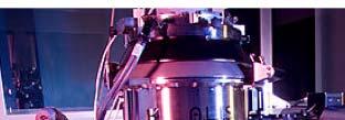
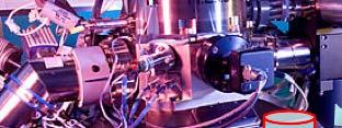
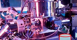
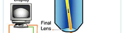
11 Focused Ion Beam
12 Ga Focused Ion Beam Machining
13 Machining with Gallium Ions Benefits: Rapid R id M Material t i l Removal
14 Machining with Neon Ions Benefits: Precise Materia Removal No Ga Implantation 200nm
15 Machining with Helium Ions Benefits: Nanofabrication (<10nm) Minimal Lateral Damage ~4nm gap 100nm TEM Image
16 Imaging with Helium Ions Benefits: High Resolution (0.50 nm) No Charging Artifacts Large Depth of Field 500nm Pd catalyst grown on ZnO nanowires
17 Multi-ion beam machining Ga Milling Ne Milling Intermediate Final Bulk Milling Milling with with Ga He Ne He Milling Sample: Gold film on Glass substrate
18
19
20
21
22
23 Ion Beam Lithography Application Sub-10 nm Lithography Solution Helium Ion Beam Lithography. State-of-the-art He-Beam Litho Best results : 4 nm lines at 7 nm pitch Half-pitch = 5 nm Dose = 68 ions/nm Half-pitch = 4 nm Dose = 56 ions/nm Half-pitch = 3.5 nm Dose = 49 ions/nm Source: Karl Berggren, MIT Donny Winston, HP Extending the limits
24
25 Key Research Challenges Create & demonstrate new production chains to apply nano & micro scale features rapidly onto large (and continuous) multi-material substrates, through flag ship projects creating 3 research platforms. Create & demonstrate new ultra precision and fine feature generation processes for multi- material processing of emerging smart products including their effective quality control.
26
27
28 Nano Fabrication Platform Technology Productivity it ~ x 30, over FIB


29 Hybrid FIB/Laser/RAP
30 The Alpha Factory The Alpha Factory would serve as a hub for innovation and manufacturing technology development and company scale up and would actively identify and provide services required to support client's success. Preliminary objectives for the Centre may include the following: Assist the commercialisation of emerging innovation Support the development of advanced manufacturing technologies Create new job opportunities for Cambridge area residents and those in the wider UK Better leverage of intellectual property p from universities, research laboratories and companies Generate new innovation models for the UK
31 Bibliography 1. CMOS Process Flow in Wafer Fab, Semiconductor Manufacturing Technology, DRAFT, Austin Community College, January 2, Semiconductor ctor Processing with MKS Instruments, Inc. 3. Worthington, Eric. New CMP architecture addresses key process issues, Solid State Technology, January Leskonic, Sharon. Overview of CMP Processing, SEMATECH Presentation, Gwozdz, Peter. Semiconductor Processing Technology SEMI, CVD Tungsten, Novellus Sales Brochure, 7/ Fullman Company website. Fullman Company - The Semiconductor Manufacturing Process, ctors/inde html Barrett, Craig R. From Sand to Silicon: Manufacturing an Integrated Circuit, Scientific American Special Issue: The Solid State Century, January 22,
32 Thank-you
Intel Technology Journal
 Volume 06 Issue 02 Published, May 16, 2002 ISSN 1535766X Intel Technology Journal Semiconductor Technology and Manufacturing The Intel Lithography Roadmap A compiled version of all papers from this issue
write-nanocircuits Direct-write Jaebum Joo and Joseph M. Jacobson Molecular Machines, Media Lab Massachusetts Institute of Technology, Cambridge, MA
 Fab-in in-a-box: Direct-write write-nanocircuits Jaebum Joo and Joseph M. Jacobson Massachusetts Institute of Technology, Cambridge, MA April 17, 2008 Avogadro Scale Computing / 1 Avogadro number s? Intel
Light Sources for EUV Mask Metrology. Heiko Feldmann, Ulrich Müller
 Light Sources for EUV Mask Metrology Heiko Feldmann, Ulrich Müller Dublin, October 9, 2012 Agenda 1 2 3 4 Actinic Metrology in Mask Making The AIMS EUV Concept Metrology Performance Drivers and their Relation
Optics for EUV Lithography
 Optics for EUV Lithography Dr. Sascha Migura, Carl Zeiss SMT GmbH, Oberkochen, Germany 2018 EUVL Workshop June 13 th, 2018 Berkeley, CA, USA The resolution of the optical system determines the minimum
Module - 2 Lecture - 13 Lithography I
 Nano Structured Materials-Synthesis, Properties, Self Assembly and Applications Prof. Ashok. K.Ganguli Department of Chemistry Indian Institute of Technology, Delhi Module - 2 Lecture - 13 Lithography
Ion Beam Lithography next generation nanofabrication
 Ion Beam Lithography next generation nanofabrication EFUG Bordeaux 2011 ion beams develop Lloyd Peto IBL sales manager Copyright 2011 by Raith GmbH ionline new capabilities You can now Apply an ion beam
Discovering Electrical & Computer Engineering. Carmen S. Menoni Professor Week 3 armain.
 Discovering Electrical & Computer Engineering Carmen S. Menoni Professor Week 3 http://www.engr.colostate.edu/ece103/semin armain.html TOP TECH 2012 SPECIAL REPORT IEEE SPECTRUM PAGE 28, JANUARY 2012 P.E.
MAPPER: High throughput Maskless Lithography
 MAPPER: High throughput Maskless Lithography Marco Wieland CEA- Leti Alterative Lithography workshop 1 Today s agenda Introduction Applications Qualification of on-tool metrology by in-resist metrology
5. Lithography. 1. photolithography intro: overall, clean room 2. principle 3. tools 4. pattern transfer 5. resolution 6. next-gen
 5. Lithography 1. photolithography intro: overall, clean room 2. principle 3. tools 4. pattern transfer 5. resolution 6. next-gen References: Semiconductor Devices: Physics and Technology. 2 nd Ed. SM
Intel's 65 nm Logic Technology Demonstrated on 0.57 µm 2 SRAM Cells
 Intel's 65 nm Logic Technology Demonstrated on 0.57 µm 2 SRAM Cells Mark Bohr Intel Senior Fellow Director of Process Architecture & Integration Intel 1 What are We Announcing? Intel has fabricated fully-functional
Progress due to: Feature size reduction - 0.7X/3 years (Moore s Law). Increasing chip size - 16% per year. Creativity in implementing functions.
. Increasing chip size - 16% per year. Creativity in implementing functions.") Introduction - Chapter 1 Evolution of IC Fabrication 1960 and 1990 integrated t circuits. it Progress due to: Feature size reduction - 0.7X/3 years (Moore s Law). Increasing chip size - 16% per year. Creativity
Introduction - Chapter 1 Evolution of IC Fabrication 1960 and 1990 integrated t circuits. it Progress due to: Feature size reduction - 0.7X/3 years (Moore s Law). Increasing chip size - 16% per year. Creativity
Chapter 17: Wave Optics. What is Light? The Models of Light 1/11/13
 Chapter 17: Wave Optics Key Terms Wave model Ray model Diffraction Refraction Fringe spacing Diffraction grating Thin-film interference What is Light? Light is the chameleon of the physical world. Under
UV Nanoimprint Stepper Technology: Status and Roadmap. S.V. Sreenivasan Sematech Litho Forum May 14 th, 2008
 UV Nanoimprint Stepper Technology: Status and Roadmap S.V. Sreenivasan Sematech Litho Forum May 14 th, 2008 Overview Introduction Stepper technology status: Patterning and CD Control Through Etch Alignment
Photolithography I ( Part 1 )
") 1 Photolithography I ( Part 1 ) Chapter 13 : Semiconductor Manufacturing Technology by M. Quirk & J. Serda Bjørn-Ove Fimland, Department of Electronics and Telecommunication, Norwegian University of Science
1 Photolithography I ( Part 1 ) Chapter 13 : Semiconductor Manufacturing Technology by M. Quirk & J. Serda Bjørn-Ove Fimland, Department of Electronics and Telecommunication, Norwegian University of Science
A Brief Introduction to Single Electron Transistors. December 18, 2011
 A Brief Introduction to Single Electron Transistors Diogo AGUIAM OBRECZÁN Vince December 18, 2011 1 Abstract Transistor integration has come a long way since Moore s Law was first mentioned and current
Nanofabrication technologies: high-throughput for tomorrow s metadevices
 Nanofabrication technologies: high-throughput for tomorrow s metadevices Rob Eason Ben Mills, Matthias Feinaugle, Dan Heath, David Banks, Collin Sones, James Grant-Jacob, Ioannis Katis. Fabrication fundamentals
Lecture: Integration of silicon photonics with electronics. Prepared by Jean-Marc FEDELI CEA-LETI
 Lecture: Integration of silicon photonics with electronics Prepared by Jean-Marc FEDELI CEA-LETI Context The goal is to give optical functionalities to electronics integrated circuit (EIC) The objectives
FinFET vs. FD-SOI Key Advantages & Disadvantages
 FinFET vs. FD-SOI Key Advantages & Disadvantages Amiad Conley Technical Marketing Manager Process Diagnostics & Control, Applied Materials ChipEx-2014, Apr 2014 1 Moore s Law The number of transistors
Lecture 7. Lithography and Pattern Transfer. Reading: Chapter 7
 Lecture 7 Lithography and Pattern Transfer Reading: Chapter 7 Used for Pattern transfer into oxides, metals, semiconductors. 3 types of Photoresists (PR): Lithography and Photoresists 1.) Positive: PR
EUV Interference Lithography in NewSUBARU
 EUV Interference Lithography in NewSUBARU Takeo Watanabe 1, Tae Geun Kim 2, Yasuyuki Fukushima 1, Noki Sakagami 1, Teruhiko Kimura 1, Yoshito Kamaji 1, Takafumi Iguchi 1, Yuuya Yamaguchi 1, Masaki Tada
Introduction of New Products
 Field Emission Electron Microscope JEM-3100F For evaluation of materials in the fields of nanoscience and nanomaterials science, TEM is required to provide resolution and analytical capabilities that can
Semiconductor Manufacturing Technology. Semiconductor Manufacturing Technology. Photolithography: Resist Development and Advanced Lithography
 Semiconductor Manufacturing Technology Michael Quirk & Julian Serda October 2001 by Prentice Hall Chapter 15 Photolithography: Resist Development and Advanced Lithography Eight Basic Steps of Photolithography
Laser patterning and projection lithography
 Introduction to Nanofabrication Techniques: Laser patterning and projection lithography Benjamin Johnston Macquarie University David O Connor Bandwidth Foundry - USYD The OptoFab node of ANFF Broad ranging
Laser-Produced Sn-plasma for Highvolume Manufacturing EUV Lithography
 Panel discussion Laser-Produced Sn-plasma for Highvolume Manufacturing EUV Lithography Akira Endo * Extreme Ultraviolet Lithography System Development Association Gigaphoton Inc * 2008 EUVL Workshop 11
Part 5-1: Lithography
 Part 5-1: Lithography Yao-Joe Yang 1 Pattern Transfer (Patterning) Types of lithography systems: Optical X-ray electron beam writer (non-traditional, no masks) Two-dimensional pattern transfer: limited
k λ NA Resolution of optical systems depends on the wavelength visible light λ = 500 nm Extreme ultra-violet and soft x-ray light λ = 1-50 nm
 Resolution of optical systems depends on the wavelength visible light λ = 500 nm Spatial Resolution = k λ NA EUV and SXR microscopy can potentially resolve full-field images with 10-100x smaller features
Optical lithography is the technique for
 By Chris A. Mack Snapshot: The author describes optical lithography in the context of the semiconductor industry. Past trends are evaluated and used to predict future possibilities. The economics of the
Silicon Photonics Photo-Detector Announcement. Mario Paniccia Intel Fellow Director, Photonics Technology Lab
 Silicon Photonics Photo-Detector Announcement Mario Paniccia Intel Fellow Director, Photonics Technology Lab Agenda Intel s Silicon Photonics Research 40G Modulator Recap 40G Photodetector Announcement
Strategies for low cost imprint molds
 Strategies for low cost imprint molds M.P.C. Watts, Impattern Solutions, 9404 Bell Mountain Drive Austin TX 78730 www.impattern.com ABSTRACT The Cost of ownership (COO) due to the mold can be minimized
Fabrication of micro structures on curve surface by X-ray lithography
 Fabrication of micro structures on curve surface by X-ray lithography Yigui Li 1, Susumu Sugiyama 2 Abstract We demonstrate experimentally the x-ray lithography techniques to fabricate micro structures
Section 2: Lithography. Jaeger Chapter 2. EE143 Ali Javey Slide 5-1
 Section 2: Lithography Jaeger Chapter 2 EE143 Ali Javey Slide 5-1 The lithographic process EE143 Ali Javey Slide 5-2 Photolithographic Process (a) (b) (c) (d) (e) (f) (g) Substrate covered with silicon
Electron Multi-Beam Technology for Mask and Wafer Direct Write. Elmar Platzgummer IMS Nanofabrication AG
 Electron Multi-Beam Technology for Mask and Wafer Direct Write Elmar Platzgummer IMS Nanofabrication AG Contents 2 Motivation for Multi-Beam Mask Writer (MBMW) MBMW Tool Principles and Architecture MBMW
Lithography. 3 rd. lecture: introduction. Prof. Yosi Shacham-Diamand. Fall 2004
 Lithography 3 rd lecture: introduction Prof. Yosi Shacham-Diamand Fall 2004 1 List of content Fundamental principles Characteristics parameters Exposure systems 2 Fundamental principles Aerial Image Exposure
Practical Applications of Laser Technology for Semiconductor Electronics
 Practical Applications of Laser Technology for Semiconductor Electronics MOPA Single Pass Nanosecond Laser Applications for Semiconductor / Solar / MEMS & General Manufacturing Mark Brodsky US Application
CMOL: Hybrid of CMOS with Overlaid Nanogrid and Nanodevice Structure. John Zacharkow
 CMOL: Hybrid of CMOS with Overlaid Nanogrid and Nanodevice Structure John Zacharkow Overview Introduction Background CMOS Review CMOL Breakdown Benefits/Shortcoming Looking into the Future Introduction
Optical Bus for Intra and Inter-chip Optical Interconnects
 Optical Bus for Intra and Inter-chip Optical Interconnects Xiaolong Wang Omega Optics Inc., Austin, TX Ray T. Chen University of Texas at Austin, Austin, TX Outline Perspective of Optical Backplane Bus
MICROCHIP MANUFACTURING by S. Wolf
 MICROCHIP MANUFACTURING by S. Wolf Chapter 19 LITHOGRAPHY II: IMAGE-FORMATION and OPTICAL HARDWARE 2004 by LATTICE PRESS CHAPTER 19 - CONTENTS Preliminaries: Wave- Motion & The Behavior of Light Resolution
Diffraction, Fourier Optics and Imaging
 1 Diffraction, Fourier Optics and Imaging 1.1 INTRODUCTION When wave fields pass through obstacles, their behavior cannot be simply described in terms of rays. For example, when a plane wave passes through
ASCENT Overview. European Nanoelectronics Infrastructure Access. MOS-AK Workshop, Infineon, Munich, 13 th March 2018.
 ASCENT Overview MOS-AK Workshop, Infineon, Munich, 13 th March 2018 European Nanoelectronics Infrastructure Access Paul Roseingrave The Challenge Cost/performance returns by scaling are diminishing Cost
(Complementary E-Beam Lithography)
") Extending Optical Lithography with C E B L (Complementary E-Beam Lithography) July 13, 2011 4008 Burton Drive, Santa Clara, CA 95054 Outline Complementary Lithography E-Beam Complements Optical Multibeam
Extending Optical Lithography with C E B L (Complementary E-Beam Lithography) July 13, 2011 4008 Burton Drive, Santa Clara, CA 95054 Outline Complementary Lithography E-Beam Complements Optical Multibeam
Major Fabrication Steps in MOS Process Flow
 Major Fabrication Steps in MOS Process Flow UV light Mask oxygen Silicon dioxide photoresist exposed photoresist oxide Silicon substrate Oxidation (Field oxide) Photoresist Coating Mask-Wafer Alignment
EE-527: MicroFabrication
 EE-57: MicroFabrication Exposure and Imaging Photons white light Hg arc lamp filtered Hg arc lamp excimer laser x-rays from synchrotron Electrons Ions Exposure Sources focused electron beam direct write
Recent Activities of the Actinic Mask Inspection using the EUV microscope at Center for EUVL
 Recent Activities of the Actinic Mask Inspection using the EUV microscope at Center for EUVL Takeo Watanabe, Tetsuo Harada, and Hiroo Kinoshita Center for EUVL, University of Hyogo Outline 1) EUV actinic
Integrated Photonics using the POET Optical InterposerTM Platform
 Integrated Photonics using the POET Optical InterposerTM Platform Dr. Suresh Venkatesan CIOE Conference Shenzhen, China Sept. 5, 2018 POET Technologies Inc. TSXV: PUBLIC POET PTK.V Technologies Inc. PUBLIC
Direct printing tools for flexible hybrid electronics assembly. David Grierson, Ph.D. President & CTO of systemech, LLC
 Direct printing tools for flexible hybrid electronics assembly David Grierson, Ph.D. President & CTO of systemech, LLC We solve the problem of placing ultra-thin, high-performance Si devices onto flexible
Feature-level Compensation & Control
 Feature-level Compensation & Control 2 Sensors and Control Nathan Cheung, Kameshwar Poolla, Costas Spanos Workshop 11/19/2003 3 Metrology, Control, and Integration Nathan Cheung, UCB SOI Wafers Multi wavelength
EUV Micro-Exposure Tool (MET) for Near-Term Development Using a High NA Projection System
 for Near-Term Development Using a High NA Projection System") EUV Micro-Exposure Tool (MET) for Near-Term Development Using a High NA Projection System John S. Taylor, Donald Sweeney, Russell Hudyma Layton Hale, Todd Decker Lawrence Livermore National Laboratory
EUV Micro-Exposure Tool (MET) for Near-Term Development Using a High NA Projection System John S. Taylor, Donald Sweeney, Russell Hudyma Layton Hale, Todd Decker Lawrence Livermore National Laboratory
Silicon on Insulator (SOI) Spring 2018 EE 532 Tao Chen
 Spring 2018 EE 532 Tao Chen") Silicon on Insulator (SOI) Spring 2018 EE 532 Tao Chen What is Silicon on Insulator (SOI)? SOI silicon on insulator, refers to placing a thin layer of silicon on top of an insulator such as SiO2. The devices
Silicon on Insulator (SOI) Spring 2018 EE 532 Tao Chen What is Silicon on Insulator (SOI)? SOI silicon on insulator, refers to placing a thin layer of silicon on top of an insulator such as SiO2. The devices
Progresses in NIL Template Fabrication Naoya Hayashi
 Progresses in NIL Template Fabrication Naoya Hayashi Electronic Device Operations Dai Nippon Printing Co., Ltd. Contents 1. Introduction Motivation NIL mask fabrication process 2. NIL mask resolution improvement
A Laser-Based Thin-Film Growth Monitor
 TECHNOLOGY by Charles Taylor, Darryl Barlett, Eric Chason, and Jerry Floro A Laser-Based Thin-Film Growth Monitor The Multi-beam Optical Sensor (MOS) was developed jointly by k-space Associates (Ann Arbor,
Photolithography 光刻 Part I: Optics
 微纳光电子材料与器件工艺原理 Photolithography 光刻 Part I: Optics Xing Sheng 盛兴 Department of Electronic Engineering Tsinghua University xingsheng@tsinghua.edu.cn 1 Integrate Circuits Moore's law transistor number transistor
Lecture 5. Optical Lithography
 Lecture 5 Optical Lithography Intro For most of microfabrication purposes the process (e.g. additive, subtractive or implantation) has to be applied selectively to particular areas of the wafer: patterning
Micro-Nanofabrication
 Zheng Cui Micro-Nanofabrication TECHNOLOGIES AND APPLICATIONS ^f**"?* ö Springer Higher Education Press -T O Table of Content Preface About the Author Chapter 1 Introduction 1 1.1 Micro-nanotechnologies
Micro- and Nano-Technology... for Optics
 Micro- and Nano-Technology...... for Optics 3.2 Lithography U.D. Zeitner Fraunhofer Institut für Angewandte Optik und Feinmechanik Jena Printing on Stones Map of Munich Stone Print Contact Printing light
32nm High-K/Metal Gate Version Including 2nd Generation Intel Core processor family
 From Sand to Silicon Making of a Chip Illustrations 32nm High-K/Metal Gate Version Including 2nd Generation Intel Core processor family April 2011 1 The illustrations on the following foils are low resolution
2D silicon-based surface-normal vertical cavity photonic crystal waveguide array for high-density optical interconnects
 2D silicon-based surface-normal vertical cavity photonic crystal waveguide array for high-density optical interconnects JaeHyun Ahn a, Harish Subbaraman b, Liang Zhu a, Swapnajit Chakravarty b, Emanuel
Institute of Solid State Physics. Technische Universität Graz. Lithography. Peter Hadley
 Technische Universität Graz Institute of Solid State Physics Lithography Peter Hadley http://www.cleanroom.byu.edu/virtual_cleanroom.parts/lithography.html http://www.cleanroom.byu.edu/su8.phtml Spin coater
Georgia Tech IEN EBL Facility NNIN Highlights 2014 External User Projects
 Georgia Tech IEN EBL Facility NNIN Highlights 2014 External User Projects Silicon based Photonic Crystal Devices Silicon based photonic crystal devices are ultra-small photonic devices that can confine
Session 2: Silicon and Carbon Photonics (11:00 11:30, Huxley LT311)
") Session 2: Silicon and Carbon Photonics (11:00 11:30, Huxley LT311) (invited) Formation and control of silicon nanocrystals by ion-beams for photonic applications M Halsall The University of Manchester,
Session 2: Silicon and Carbon Photonics (11:00 11:30, Huxley LT311) (invited) Formation and control of silicon nanocrystals by ion-beams for photonic applications M Halsall The University of Manchester,
Monolithically integrated InGaAs nanowires on 3D. structured silicon-on-insulator as a new platform for. full optical links
 Monolithically integrated InGaAs nanowires on 3D structured silicon-on-insulator as a new platform for full optical links Hyunseok Kim 1, Alan C. Farrell 1, Pradeep Senanayake 1, Wook-Jae Lee 1,* & Diana.
New Process Technologies Will silicon CMOS carry us to the end of the Roadmap?
 HPEC Workshop 2006 New Process Technologies Will silicon CMOS carry us to the end of the Roadmap? Craig L. Keast, Chenson Chen, Mike Fritze, Jakub Kedzierski, Dave Shaver HPEC 2006-1 Outline A brief history
Corporate Introduction of CRESTEC CORPORATION Expert in E-Beam Nanofabrication
 Corporate Introduction of CRESTEC CORPORATION Expert in E-Beam Nanofabrication David López-Romero Moraleda. Technical Support Manager, Crestec Corporation Spain Branch. Financiación-Internacionalización-Cooperación.
DTU DANCHIP an open access micro/nanofabrication facility bridging academic research and small scale production
 DTU DANCHIP an open access micro/nanofabrication facility bridging academic research and small scale production DTU Danchip National Center for Micro- and Nanofabrication DTU Danchip DTU Danchip is Denmark
Optical Monitoring System Enables Greater Accuracy in Thin-Film Coatings. Line Scan Cameras What Do They Do?
 November 2017 Optical Monitoring System Enables Greater Accuracy in Thin-Film Coatings Line Scan Cameras What Do They Do? Improved Surface Characterization with AFM Imaging Supplement to Tech Briefs CONTENTS
420 Intro to VLSI Design
 Dept of Electrical and Computer Engineering 420 Intro to VLSI Design Lecture 0: Course Introduction and Overview Valencia M. Joyner Spring 2005 Getting Started Syllabus About the Instructor Labs, Problem
G450C. Global 450mm Consortium at CNSE. Michael Liehr, General Manager G450C, Vice President for Research
 Global 450mm Consortium at CNSE Michael Liehr, General Manager G450C, Vice President for Research - CNSE Overview - G450C Vision - G450C Mission - Org Structure - Scope - Timeline The Road Ahead for Nano-Fabrication
The future of lithography and its impact on design
 The future of lithography and its impact on design Chris Mack www.lithoguru.com 1 Outline History Lessons Moore s Law Dennard Scaling Cost Trends Is Moore s Law Over? Litho scaling? The Design Gap The
Fabricating 2.5D, 3D, 5.5D Devices
 Fabricating 2.5D, 3D, 5.5D Devices Bob Patti, CTO rpatti@tezzaron.com Tezzar on Semiconduct or 04/15/2013 1 Gen4 Dis-Integrated 3D Memory DRAM layers 42nm node 2 million vertical connections per lay per
FABRICATION OF CMOS INTEGRATED CIRCUITS. Dr. Mohammed M. Farag
 FABRICATION OF CMOS INTEGRATED CIRCUITS Dr. Mohammed M. Farag Outline Overview of CMOS Fabrication Processes The CMOS Fabrication Process Flow Design Rules Reference: Uyemura, John P. "Introduction to
EUVL Activities in China. Xiangzhao Wang Shanghai Inst. Of Opt. and Fine Mech. Of CAS. (SIOM) Shanghai, China.
 Shanghai, China.") EUVL Activities in China Xiangzhao Wang Shanghai Inst. Of Opt. and Fine Mech. Of CAS. (SIOM) Shanghai, China. wxz26267@siom.ac.cn Projection Optics Imaging System Surface Testing Optical Machining ML Coating
EUVL Activities in China Xiangzhao Wang Shanghai Inst. Of Opt. and Fine Mech. Of CAS. (SIOM) Shanghai, China. wxz26267@siom.ac.cn Projection Optics Imaging System Surface Testing Optical Machining ML Coating
MEDIA RELEASE FOR IMMEDIATE RELEASE 26 JULY 2016
 MEDIA RELEASE FOR IMMEDIATE RELEASE 26 JULY 2016 A*STAR S IME KICKS OFF CONSORTIA TO DEVELOP ADVANCED PACKAGING SOLUTIONS FOR NEXT-GENERATION INTERNET OF THINGS APPLICATIONS AND HIGH-PERFORMANCE WIRELESS
Transistor was first invented by William.B.Shockley, Walter Brattain and John Bardeen of Bell Labratories. In 1961, first IC was introduced.
 Unit 1 Basic MOS Technology Transistor was first invented by William.B.Shockley, Walter Brattain and John Bardeen of Bell Labratories. In 1961, first IC was introduced. Levels of Integration:- i) SSI:-
Nanofluidic Diodes based on Nanotube Heterojunctions
 Supporting Information Nanofluidic Diodes based on Nanotube Heterojunctions Ruoxue Yan, Wenjie Liang, Rong Fan, Peidong Yang 1 Department of Chemistry, University of California, Berkeley, CA 94720, USA
Solid Immersion and Evanescent Wave Lithography at Numerical Apertures > 1.60
 Solid Immersion and Evanescent Wave Lithography at Numerical Apertures > 1.60 Bruce Smith Y. Fan, J. Zhou, L. Zavyalova, M. Slocum, J. Park, A. Bourov, E. Piscani, N. Lafferty, A. Estroff Rochester Institute
Low-cost Interference Lithography
 Low-cost Interference Lithography 343 Corey P. Fucetola, Hasan Korre and Karl K. Berggren Research Laboratory of Electronics Massachusetts Institute of Technology, Cambridge, MA, 02139 Abstract We report
Nanotechnology, the infrastructure, and IBM s research projects
 Nanotechnology, the infrastructure, and IBM s research projects Dr. Paul Seidler Coordinator Nanotechnology Center, IBM Research - Zurich Nanotechnology is the understanding and control of matter at dimensions
Closed Loop Registration Control (RegC ) Using PROVE as the Data Source for the RegC Process
 Using PROVE as the Data Source for the RegC Process") Invited Paper Closed Loop Registration Control (RegC ) Using PROVE as the Data Source for the RegC Process Erez Graitzer 1 ; Avi Cohen 1 ; Vladimir Dmitriev 1 ; Itamar Balla 1 ; Dan Avizemer 1 Dirk Beyer
Invited Paper Closed Loop Registration Control (RegC ) Using PROVE as the Data Source for the RegC Process Erez Graitzer 1 ; Avi Cohen 1 ; Vladimir Dmitriev 1 ; Itamar Balla 1 ; Dan Avizemer 1 Dirk Beyer
Update on 193nm immersion exposure tool
 Update on 193nm immersion exposure tool S. Owa, H. Nagasaka, Y. Ishii Nikon Corporation O. Hirakawa and T. Yamamoto Tokyo Electron Kyushu Ltd. January 28, 2004 Litho Forum 1 What is immersion lithography?
Section 2: Lithography. Jaeger Chapter 2 Litho Reader. The lithographic process
 Section 2: Lithography Jaeger Chapter 2 Litho Reader The lithographic process Photolithographic Process (a) (b) (c) (d) (e) (f) (g) Substrate covered with silicon dioxide barrier layer Positive photoresist
Midaz Micro-Slab DPSS Lasers:
 Midaz Micro-Slab DPSS Lasers: Higher power & pulse rate for higher speed micromachining Professor Mike Damzen Midaz Laser Ltd 4 June 2008 AILU Meeting Industrial opportunities in laser micro and nano processing
DTU DANCHIP an open access micro/nanofabrication facility bridging academic research and small scale production
 DTU DANCHIP an open access micro/nanofabrication facility bridging academic research and small scale production DTU Danchip National Center for Micro- and Nanofabrication DTU Danchip DTU Danchip is Denmark
Open Innovation to Manage Risks in Technology The Business of Breakthroughs
 Open Innovation to Manage Risks in Technology The Business of Breakthroughs Janos Veres, Program Manager 2016 PARC, All rights reserved. PARC Legacy: A Storied History of Inventing the Future 1970 1973
Section 2: Lithography. Jaeger Chapter 2 Litho Reader. EE143 Ali Javey Slide 5-1
 Section 2: Lithography Jaeger Chapter 2 Litho Reader EE143 Ali Javey Slide 5-1 The lithographic process EE143 Ali Javey Slide 5-2 Photolithographic Process (a) (b) (c) (d) (e) (f) (g) Substrate covered
Moving from biomedical to industrial applications: OCT Enables Hi-Res ND Depth Analysis
 Moving from biomedical to industrial applications: OCT Enables Hi-Res ND Depth Analysis Patrick Merken a,c, Hervé Copin a, Gunay Yurtsever b, Bob Grietens a a Xenics NV, Leuven, Belgium b UGENT, Ghent,
The End of Thresholds: Subwavelength Optical Linewidth Measurement Using the Flux-Area Technique
 The End of Thresholds: Subwavelength Optical Linewidth Measurement Using the Flux-Area Technique Peter Fiekowsky Automated Visual Inspection, Los Altos, California ABSTRACT The patented Flux-Area technique
Nanostencil Lithography and Nanoelectronic Applications
 Microsystems Laboratory Nanostencil Lithography and Nanoelectronic Applications Oscar Vazquez, Marc van den Boogaart, Dr. Lianne Doeswijk, Prof. Juergen Brugger, LMIS1 Dr. Chan Woo Park, Visiting Professor
Roadmap Semiconductor Equipment Innovation Agenda
 Roadmap Semiconductor Equipment Innovation Agenda 2018-2021 1. Societal and economic relevance Over the years, electronics have become an inseparable part of our lives. Think of the internet, the cloud,
The Department of Advanced Materials Engineering. Materials and Processes in Polymeric Microelectronics
 The Department of Advanced Materials Engineering Materials and Processes in Polymeric Microelectronics 1 Outline Materials and Processes in Polymeric Microelectronics Polymeric Microelectronics Process
Integrated into Nanowire Waveguides
 Supporting Information Widely Tunable Distributed Bragg Reflectors Integrated into Nanowire Waveguides Anthony Fu, 1,3 Hanwei Gao, 1,3,4 Petar Petrov, 1, Peidong Yang 1,2,3* 1 Department of Chemistry,
New CD-SEM System for 100-nm Node Process
 New CD-SEM System for 100-nm Node Process Hitachi Review Vol. 51 (2002), No. 4 125 Osamu Nasu Katsuhiro Sasada Mitsuji Ikeda Makoto Ezumi OVERVIEW: With the semiconductor device manufacturing industry
Chapter 2 Silicon Planar Processing and Photolithography
 Chapter 2 Silicon Planar Processing and Photolithography The success of the electronics industry has been due in large part to advances in silicon integrated circuit (IC) technology based on planar processing,
Design and Fabrication of an Efficient Extreme Ultraviolet Beam Splitter
 EUV Beam Splitter 1 Design and Fabrication of an Efficient Extreme Ultraviolet Beam Splitter First Semester Report Full Report By: Andrew Wiley Maram Alfaraj Prepared to partially fulfill the requirements
NANOFABRICATION, THE NEW GENERATION OF LITHOGRAPHY. Cheng-Sheng Huang & Alvin Chang ABSTRACT
 NANOFABRICATION, THE NEW GENERATION OF LITHOGRAPHY Cheng-Sheng Huang & Alvin Chang ABSTRACT Fabrication on the micro- and nano-structure has opened the new horizons in science and engineering. The success
OPTI510R: Photonics. Khanh Kieu College of Optical Sciences, University of Arizona Meinel building R.626
 OPTI510R: Photonics Khanh Kieu College of Optical Sciences, University of Arizona kkieu@optics.arizona.edu Meinel building R.626 Announcements Homework #3 is due today No class Monday, Feb 26 Pre-record
INSPECTION AND REVIEW PORTFOLIO FOR 3D FUTURE
 INSPECTION AND REVIEW PORTFOLIO FOR 3D FUTURE This week announced updates to four systems the 2920 Series, Puma 9850, Surfscan SP5 and edr-7110 intended for defect inspection and review of 16/14nm node
Design and fabrication of indium phosphide air-bridge waveguides with MEMS functionality
 Design and fabrication of indium phosphide air-bridge waveguides with MEMS functionality Wing H. Ng* a, Nina Podoliak b, Peter Horak b, Jiang Wu a, Huiyun Liu a, William J. Stewart b, and Anthony J. Kenyon
Manufacturing Case Studies: Copy Exactly (CE!) and the two-year cycle at Intel
 and the two-year cycle at Intel") Manufacturing Case Studies: Copy Exactly (CE!) and the two-year cycle at Intel Paolo A. Gargini Director Technology Strategy Intel Fellow 1 Agenda 2-year cycle Copy Exactly Conclusions 2 I see no reason
Manufacturing Case Studies: Copy Exactly (CE!) and the two-year cycle at Intel Paolo A. Gargini Director Technology Strategy Intel Fellow 1 Agenda 2-year cycle Copy Exactly Conclusions 2 I see no reason
Directional Growth of Ultra-long CsPbBr 3 Perovskite. Nanowires for High Performance Photodetectors
 Supporting information Directional Growth of Ultra-long CsPbBr 3 Perovskite Nanowires for High Performance Photodetectors Muhammad Shoaib, Xuehong Zhang, Xiaoxia Wang, Hong Zhou, Tao Xu, Xiao Wang, Xuelu
From Sand to Silicon Making of a Chip Illustrations May 2009
 From Sand to Silicon Making of a Chip Illustrations May 2009 1 The illustrations on the following foils are low resolution images that visually support the explanations of the individual steps. For publishing
Welcome to. A facility within the Nanometer Structure Consortium (nmc) at Lund University. nanolab. lund
 at Lund University. nanolab. lund") lund nanolab Welcome to A facility within the Nanometer Structure Consortium (nmc) at Lund University »It s a dream come true. This is the lab I always dreamt of. I didn t know it would ever exist.«ivan
lund nanolab Welcome to A facility within the Nanometer Structure Consortium (nmc) at Lund University »It s a dream come true. This is the lab I always dreamt of. I didn t know it would ever exist.«ivan