Open Innovation to Manage Risks in Technology The Business of Breakthroughs
|
|
|
- Barbra Atkins
- 5 years ago
- Views:
Transcription


1 Open Innovation to Manage Risks in Technology The Business of Breakthroughs Janos Veres, Program Manager 2016 PARC, All rights reserved.


2 PARC Legacy: A Storied History of Inventing the Future Xerox PARC PC - Alto WYSIWYG GUI Multi-beam lasers Blue laser Biomedical systems Energy Content-centric networking Laser printing Ethernet Programming languages Ubiquitous computing Electronic reusable paper PARC, a Xerox Company Printed, flexible electronics PARC, All rights reserved.

3 Challenges of Open Innovation Not invented here Concern for control Not my market What if successful? 3


4 Focus Areas Printed Electronics Photonics Cleantech & Energy Digital Design & Manufacturing Contextual Intelligence Big Data Analytics Video & Image Analytics Content-Centric Networking Security & Privacy Innovation Services


5 PARC Business Model Internal R&D Public Sector Sponsors Ecosystem Partners Market-Facing Clients 5


6 PARC Innovation Model Multi-Disciplinary Research Human Context Understanding Holistic Business Models 6


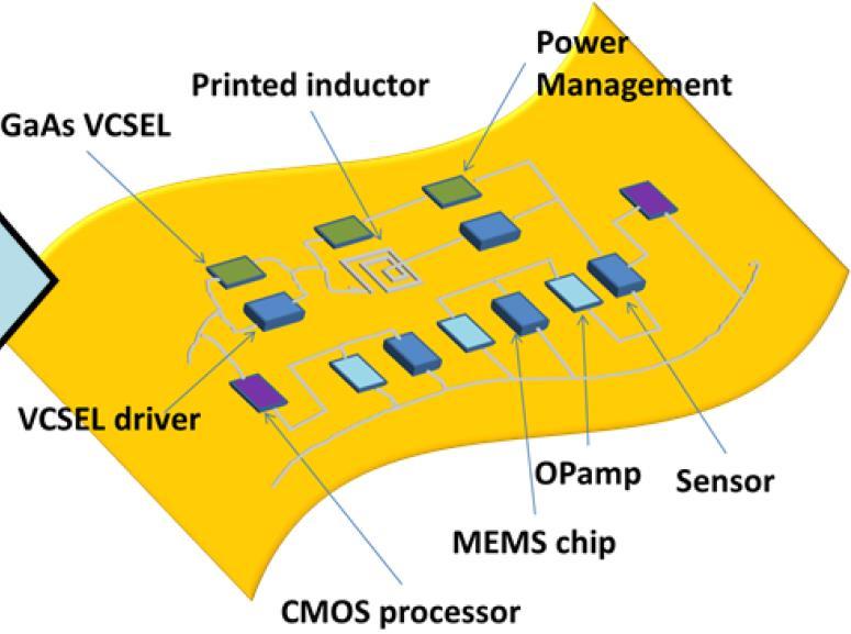
7 Future electronics Any form factor, anywhere Flexible, conformal, 3D application specific smart labels, wearables, structural electronics New levels of complexity Seamlessly integrate micro and macro; logic, chips, batteries, sensors, MEMS, photonics Easy to fabricate, on-demand Accessible, low capital, local, additive, green


8 Creating opportunities Transportation Personalized health Interactive Entertain Educate Printed Electronics Structural monitoring Supply chain Smart packaging


9 PARC s explorations into the future Large Area Electronics x-ray; fingerprints, IR imaging, thin film sensors for bio-sensing Flexible Printed and Hybrid Electronics IOT, smart labels, wearables, digital electronics fabrication System Prototyping Structural Electronics New form factors, complex integration, sensors in structures, design and workflow Morphing Electronics Moving chiplets, Vanishing electronics, Self-configuring circuits

10 Vanishing Electronics Funded by DARPA 2016 Palo Alto Research Center Incorporated; all rights PARC reserved 10


11 Gas sensor networks Outline: PARC s open innovation model Technologies accelerate and merge The future of electronics & photonics Integration Unique examples 11


12 transmission reflection reflection Embedded Fiber-Optic Sensing for Battery Packs Fiber sensors in batteries white light Photonic readout Fiber Bragg grating sensor mirror gain medium Laser cavity se n 1 λ 1 λ 1 +Δλ λ 1 stimulus n 2 fluidic channel wavelength Su Red: UDDS cycles Blue: Static cycles Photonic crystal sensor λ 1 λ 1 +Δλ wavelength λ 1 white light Silicon micro-sphere sensor 12 stimulus white light wavelength


13 Printing with microchip inks


14 Summary Future electronics is ubiquitous Increasingly merging with photonics, MEMs and its environment Serves myriads of custom use cases Opportunity to add intelligence to new product domains Open Innovation is key to navigate the unknown Technology + Human context + Business models Embedded temperature sensor Structure heath monitoring sensor Solid, low strength light weight area Optical transceiver for Optical encoder Solid, high strength area Flexible area Embedded control/ communication IC Plastic structural material Jetted and cured on the fly Embedded Ultrasonic Motor for motion PARC 14 Pre-fabbed Metal wire bone structure Assembled and welded on the fly
15 Engage with us contact PARC website sign up for updates PARC 15
the business of breakthroughs
 the business of breakthroughs breakthrough to business value Global competition is intensifying. Your customers have more options than ever before. The entire technology landscape is evolving at a staggering
FRAUNHOFER INSTITUTE FOR PHOTONIC MICROSYSTEMS IPMS. Application Area. Quality of Life
 FRAUNHOFER INSTITUTE FOR PHOTONIC MICROSYSTEMS IPMS Application Area Quality of Life Overlay image of visible spectral range (VIS) and thermal infrared range (LWIR). Quality of Life With extensive experience
The Next Industrial Revolution Industry 4.0. M.Sanne, October 2017
 The Next Industrial Revolution Industry 4.0 M.Sanne, October 2017 1 Innovation is accelerating to exponential levels by Catalytic Innovations e.g. Digitization/Digitalization Catalytic Innovations In
NTU RECIPIENTS OF NRF S PROOF OF CONCEPT SCHEME GRANTS. 1. A Semantics-Based and Service-Oriented Framework for the Virtualisation of Sensor Networks
 Reg. No. 200604393R FACT SHEET For immediate release Total: 7 pages including this page Singapore, 21 August 2009 NTU RECIPIENTS OF NRF S PROOF OF CONCEPT SCHEME GRANTS 1. A Semantics-Based and Service-Oriented
VERTICAL CAVITY SURFACE EMITTING LASER
 VERTICAL CAVITY SURFACE EMITTING LASER Nandhavel International University Bremen 1/14 Outline Laser action, optical cavity (Fabry Perot, DBR and DBF) What is VCSEL? How does VCSEL work? How is it different
Accelerating Scale Up of Large Area Electronics
 Accelerating Scale Up of Large Area Electronics Duncan Lindsay Business Development Director, CPI 2015 Centre for Process Innovation Limited. All Rights Reserved. Who are CPI? CPI is a UK technology innovation
ICT Micro- and nanoelectronics technologies
 EPoSS Proposers' Day, 2 Feb 2017, Brussels ICT 31-2017 Micro- and nanoelectronics technologies Eric Fribourg-Blanc, Henri Rajbenbach, Andreas Lymberis European Commission DG CONNECT (Communications Networks,
A Glimpse of Human-Computer Interaction. Jim Hollan Department of Cognitive Science Department of Computer Science and Engineering
 A Glimpse of Human-Computer Interaction Jim Hollan Department of Cognitive Science Department of Computer Science and Engineering Email: hollan@ucsd.edu Lab: Design Lab at UC San Diego Web: hci.ucsd.edu/hollan
MEDIA RELEASE FOR IMMEDIATE RELEASE 26 JULY 2016
 MEDIA RELEASE FOR IMMEDIATE RELEASE 26 JULY 2016 A*STAR S IME KICKS OFF CONSORTIA TO DEVELOP ADVANCED PACKAGING SOLUTIONS FOR NEXT-GENERATION INTERNET OF THINGS APPLICATIONS AND HIGH-PERFORMANCE WIRELESS
Emerging MEMS & Sensor Technologies to Watch: Alissa M. Fitzgerald, Ph.D., Founder & CEO Semicon West 2018
 Emerging MEMS & Sensor Technologies to Watch: 2018 Alissa M. Fitzgerald, Ph.D., Founder & CEO amf@amfitzgerald.com Outline About AMFitzgerald What emerging means in this presentation Emerging MEMS & sensor
Energy beam processing and the drive for ultra precision manufacturing
 Energy beam processing and the drive for ultra precision manufacturing An Exploration of Future Manufacturing Technologies in Response to the Increasing Demands and Complexity of Next Generation Smart
Faculty Development Program on Micro-Electro-Mechanical Systems (MEMS Sensor)
") Faculty Development Program on Micro-Electro-Mechanical Systems (MEMS Report MEMS sensors have been dominating the consumer products such as mobile phones, music players and other portable devices. With
Faculty Development Program on Micro-Electro-Mechanical Systems (MEMS Report MEMS sensors have been dominating the consumer products such as mobile phones, music players and other portable devices. With
GoToWebinar Housekeeping: attendee screen Lumerical Solutions, Inc.
 GoToWebinar Housekeeping: attendee screen 2012 Lumerical Solutions, Inc. GoToWebinar Housekeeping: your participation Open and hide your control panel Join audio: Choose Mic & Speakers to use VoIP Choose
E. A. MENDOZA, J. PROHASKA, C. KEMPEN, S. SUN and Y. ESTERKIN
 Fully Integrated Miniature Multi-Point Fiber Bragg Grating Sensor Interrogator (FBG-Transceiver TM ) System for Applications where Size, Weight, and Power are Critical for Operation E. A. MENDOZA, J. PROHASKA,
Fieldlab Multi-material 3D Printing 3D printed structural electronics at TNO AMSYSTEMS Center
 Fieldlab Multi-material 3D Printing 3D printed structural electronics at TNO AMSYSTEMS Center Dr. Wijnand Germs wijnand.germs@tno.nl 3DP STRUCTURAL ELECTRONICS DEMO STATUS TODAY 3DP STRUCTURAL ELECTRONICS
Silicon nitride based TriPleX Photonic Integrated Circuits for sensing applications
 Silicon nitride based TriPleX Photonic Integrated Circuits for sensing applications Arne Leinse a.leinse@lionix-int.com 2 Our chips drive your business 2 What are Photonic ICs (PICs)? Photonic Integrated
EU's contribution to research and innovation in Electronics
 EU's contribution to research and innovation in Electronics Henri.RAJBENBACH@ec.europa.eu Nikolaos.KYRLOGLOU@ec.europa.eu European Commission DG CONNECT (not legally binding presentation) SEMICON Europa-Flex
Advanced Technologies & Intelligent Autonomous Systems in Alberta. Ken Brizel CEO ACAMP
 Advanced Technologies & Intelligent Autonomous Systems in Alberta Ken Brizel CEO ACAMP Who and What is ACAMP ACAMP is a unique industry led product development centre supporting advanced technology commercialization
Micro-sensors - what happens when you make "classical" devices "small": MEMS devices and integrated bolometric IR detectors
 Micro-sensors - what happens when you make "classical" devices "small": MEMS devices and integrated bolometric IR detectors Dean P. Neikirk 1 MURI bio-ir sensors kick-off 6/16/98 Where are the targets
How material engineering contributes to delivering innovation in the hyper connected world
 How material engineering contributes to delivering innovation in the hyper connected world Paul BOUDRE, Soitec CEO Leti Innovation Days - July 2018 Grenoble, France We live in a world of data In perpetual
Roadmap for Wearable Standards
 Roadmap for Wearable Standards Jesse S. Jur Department of Textile Engineering, Chemistry & Science next (nano-extended textiles) research group Expanding the Influence of Nanotechnology in Textiles 1 2
Silicon Light Machines Patents
 820 Kifer Road, Sunnyvale, CA 94086 Tel. 408-240-4700 Fax 408-456-0708 www.siliconlight.com Silicon Light Machines Patents USPTO No. US 5,808,797 US 5,841,579 US 5,798,743 US 5,661,592 US 5,629,801 US
MEMS in ECE at CMU. Gary K. Fedder
 MEMS in ECE at CMU Gary K. Fedder Department of Electrical and Computer Engineering and The Robotics Institute Carnegie Mellon University Pittsburgh, PA 15213-3890 fedder@ece.cmu.edu http://www.ece.cmu.edu/~mems
Printing Beyond Color. Printed Smart Objects on Advanced Paper Substrates. Reinhard R. Baumann
 Printing Beyond Color Printed Smart Objects on Advanced Paper Substrates June 17, 2009 member of Reinhard R. Baumann member of Chemnitz University of Technology Institute for Print and Media Technology
Trends in Optical Transceivers:
 Trends in Optical Transceivers: Light sources for premises networks Peter Ronco Corning Optical Fiber Asst. Product Line Manager Premises Fibers January 24, 2006 Outline: Introduction: Transceivers and
Optical Bus for Intra and Inter-chip Optical Interconnects
 Optical Bus for Intra and Inter-chip Optical Interconnects Xiaolong Wang Omega Optics Inc., Austin, TX Ray T. Chen University of Texas at Austin, Austin, TX Outline Perspective of Optical Backplane Bus
Introduction Fundamentals of laser Types of lasers Semiconductor lasers
 ECE 5368 Introduction Fundamentals of laser Types of lasers Semiconductor lasers Introduction Fundamentals of laser Types of lasers Semiconductor lasers How many types of lasers? Many many depending on
Clusters in EUREKA > 2
 Clusters in EUREKA > 2 Source: EUREKA 25 year overview (2011) EUREKA clusters, status end 2011: 120 running projects with a total effort of more than 15000 PY and a total budget of more than 2 B Labelled
Winter College on Optics: Fundamentals of Photonics - Theory, Devices and Applications February 2014
 2572-10 Winter College on Optics: Fundamentals of Photonics - Theory, Devices and Applications 10-21 February 2014 Photonic packaging and integration technologies II Sonia M. García Blanco University of
Photonic Crystal Slot Waveguide Spectrometer for Detection of Methane
 Photonic Crystal Slot Waveguide Spectrometer for Detection of Methane Swapnajit Chakravarty 1, Wei-Cheng Lai 2, Xiaolong (Alan) Wang 1, Che-Yun Lin 2, Ray T. Chen 1,2 1 Omega Optics, 10306 Sausalito Drive,
Printed Electronics: success stories and future commercial applications
 Printed Electronics: success stories and future commercial applications Dr Guillaume Chansin @gchansin June 2017 Helping you profit from emerging technologies Advantages of printed electronics Mass production
sensors & systems Imagine future imaging... Leti, technology research institute Contact:
 Imaging sensors & systems Imagine future imaging... Leti, technology research institute Contact: leti.contact@cea.fr From consumer markets to high-end applications smart home IR array for human activity
09/10/18 How AI is Revolutionizing Manufacturing
 09/10/18 How AI is Revolutionizing Manufacturing CIO Magazine https://www.cio.com/article/3302797/artificial-intelligence/how-ai-is-revolutionizingmanufacturing.html Artificial intelligence and machine
NON-TRADITIONAL MACHINING PROCESSES ULTRASONIC, ELECTRO-DISCHARGE MACHINING (EDM), ELECTRO-CHEMICAL MACHINING (ECM)
, ELECTRO-CHEMICAL MACHINING (ECM)") NON-TRADITIONAL MACHINING PROCESSES ULTRASONIC, ELECTRO-DISCHARGE MACHINING (EDM), ELECTRO-CHEMICAL MACHINING (ECM) A machining process is called non-traditional if its material removal mechanism is basically
NON-TRADITIONAL MACHINING PROCESSES ULTRASONIC, ELECTRO-DISCHARGE MACHINING (EDM), ELECTRO-CHEMICAL MACHINING (ECM) A machining process is called non-traditional if its material removal mechanism is basically
National Centre for Flexible Electronics
 National Centre for Flexible Electronics Tripartite Partnership Government FlexE Centre - A platform for a meaningful interaction between industry and academia. An interdisciplinary team that advances
CREST Cluster Focus & Projects. 23rd February 2015
 CREST Cluster Focus & Projects 23rd February 2015 Domain Areas Clusters focus 1. Optoelectronics/LED and Solid State Lighting 2. Embedded System & Internet of Things 3. IC Design, Test & Validation 4.
Developing Smart Miniaturized Solutions for Industry
 Developing Smart Miniaturized Solutions for Industry Micro nanotechnologies & Embedded Software Competitive Cluster - Grenoble / France www.minalogic.com Born in Grenoble 1 st french scanner (1972) Airbag
6-7 October Marina Bay Sands Expo & Convention Centre Peony Ballroom [Level 4]
![6-7 October Marina Bay Sands Expo & Convention Centre Peony Ballroom [Level 4]](/thumbs/80/80853998.jpg "6-7 October Marina Bay Sands Expo & Convention Centre Peony Ballroom [Level 4]") camline http://www.camline.com Booth 22 camline s mission is to provide the highest quality software solutions for factory automation and logistics, helping global manufacturers maintain their competitive
camline http://www.camline.com Booth 22 camline s mission is to provide the highest quality software solutions for factory automation and logistics, helping global manufacturers maintain their competitive
EE C245 ME C218 Introduction to MEMS Design
 EE C245 ME C218 Introduction to MEMS Design Fall 2008 Prof. Clark T.-C. Nguyen Dept. of Electrical Engineering & Computer Sciences University of California at Berkeley Berkeley, CA 94720 Lecture 1: Definition
SNAPP Swiss National Applicaton Laboratory for Photonic tools and Photonic manufacturing
 SNAPP Swiss National Applicaton Laboratory for Photonic tools and Photonic manufacturing Details of SNAPP Look into the laboratories of the partner Swiss National Photonics Labs SNAPP Swiss National Applicaton
COMPUTER SCIENCE AND ENGINEERING
 COMPUTER SCIENCE AND ENGINEERING Internet of Thing Cloud Computing Big Data Analytics Network Security Distributed System Image Processing Data Science Business Intelligence Wireless Sensor Network Artificial
Reducing MEMS product development and commercialization time
 Reducing MEMS product development and commercialization time Introduction Fariborz Maseeh, Andrew Swiecki, Nora Finch IntelliSense Corporation 36 Jonspin Road, Wilmington MA 01887 www.intellisense.com
EU Research project proposals (call for Finnish companies)
") EU Research project proposals (call for Finnish companies) 11th EEMELI Workshop 29 th August 2012 Jukka Hast Research Professor VTT Technical Research Centre of Finland 04/10/2012 2 General ICT theme work
EU Research project proposals (call for Finnish companies) 11th EEMELI Workshop 29 th August 2012 Jukka Hast Research Professor VTT Technical Research Centre of Finland 04/10/2012 2 General ICT theme work
Intra-cavity active optics in lasers
 Intra-cavity active optics in lasers W. Lubeigt, A. Kelly, V. Savitsky, D. Burns Institute of Photonics, University of Strathclyde Wolfson Centre,106 Rottenrow Glasgow G4 0NW, UK J. Gomes, G. Brown, D.
Advances in Laser Micro-machining for Wafer Probing and Trimming
 Advances in Laser Micro-machining for Wafer Probing and Trimming M.R.H. Knowles, A.I.Bell, G. Rutterford & A. Webb Oxford Lasers June 10, 2002 Oxford Lasers June 2002 1 Introduction to Laser Micro-machining
Feature-level Compensation & Control
 Feature-level Compensation & Control 2 Sensors and Control Nathan Cheung, Kameshwar Poolla, Costas Spanos Workshop 11/19/2003 3 Metrology, Control, and Integration Nathan Cheung, UCB SOI Wafers Multi wavelength
SEE MORE, SMARTER. We design the most advanced vision systems to bring humanity to any device.
 SEE MORE, SMARTER OUR VISION Immervision Enables Intelligent Vision OUR MISSION We design the most advanced vision systems to bring humanity to any device. ABOUT US Immervision enables intelligent vision
Development of a MEMS-based Dielectric Mirror
 Development of a MEMS-based Dielectric Mirror A Report Submitted for the Henry Samueli School of Engineering Research Scholarship Program By ThanhTruc Nguyen June 2001 Faculty Supervisor Richard Nelson
Marking Cutting Welding Micro Machining Additive Manufacturing
 Marking Cutting Welding Micro Machining Additive Manufacturing Slide: 1 CM-F00003 Rev 4 G4 Pulsed Fiber Laser Slide: 2 CM-F00003 Rev 4 Versatility for Industry Automotive 2D/3D Cutting Night & Day Marking
Design Rules for Silicon Photonic Packaging at Tyndall Institute
 Design Rules for Silicon Photonic Packaging at Tyndall Institute January 2015 About Tyndall Institute Established with a mission to support industry and academia in driving research to market, Tyndall
Waveguide Bragg Gratings and Resonators LUMERICAL SOLUTIONS INC
 Waveguide Bragg Gratings and Resonators JUNE 2016 1 Outline Introduction Waveguide Bragg gratings Background Simulation challenges and solutions Photolithography simulation Initial design with FDTD Band
Integrated electro-optical waveguide based devices with liquid crystals on a silicon backplane
 Integrated electro-optical waveguide based devices with liquid crystals on a silicon backplane Florenta Costache Group manager Smart Micro-Optics SMO/AMS Fraunhofer Institute for Photonic Microsystems,
MEMS Spectroscopy Overview
 MEMS Spectroscopy Overview LIVING IN A SENSORY WORLD Everyday, and in so many ways, we circulate in a world of sensors. We do so mainly without knowing it. MEMS, sensors and the Internet of Things (IoT)
Accelerating Collective Innovation: Investing in the Innovation Landscape
 PCB Executive Forum Accelerating Collective Innovation: Investing in the Innovation Landscape How a Major Player Uses Internal Venture Program to Accelerate Small Players with Big Ideas Dr. Joan K. Vrtis
LUCEDA PHOTONICS DELIVERS A SILICON PHOTONICS IC SOLUTION IN TANNER L-EDIT
 LUCEDA PHOTONICS DELIVERS A SILICON PHOTONICS IC SOLUTION IN TANNER L-EDIT WIM BOGAERTS, PIETER DUMON, AND MARTIN FIERS, LUCEDA PHOTONICS JEFF MILLER, MENTOR GRAPHICS A M S D E S I G N & V E R I F I C
Здра вствуйте, това рищи!
 Manufacturing of Smart Objects by Printing Technologies Здра вствуйте, това рищи! Moscow / RUS, June 05, 2013 Reinhard R. Baumann Chemnitz University of Technology Chair of Digital Printing Fraunhofer
Introduction. Theory of Operation
 Mohan Rokkam Page 1 12/15/2004 Introduction The goal of our project is to design and build an automated shopping cart that follows a shopper around. Ultrasonic waves are used due to the slower speed of
A 3.9 ns 8.9 mw 4 4 Silicon Photonic Switch Hybrid-Integrated with CMOS Driver
 A 3.9 ns 8.9 mw 4 4 Silicon Photonic Switch Hybrid-Integrated with CMOS Driver A. Rylyakov, C. Schow, B. Lee, W. Green, J. Van Campenhout, M. Yang, F. Doany, S. Assefa, C. Jahnes, J. Kash, Y. Vlasov IBM
PILOT LINE FOR LARGE-AREA PRINTING OF ELECTRONIC AND PHOTONIC DEVICES. Simon Perraud, Ph.D. Vice president for European affairs
 PILOT LINE FOR LARGE-AREA PRINTING OF ELECTRONIC AND PHOTONIC DEVICES Simon Perraud, Ph.D. Vice president for European affairs ABOUT LITEN Liten is the research institute of CEA devoted to clean energy
PROCEEDINGS OF SPIE. H. Thienpont, J. Mohr, M. Kujawinska, M. R. Taghizadeh, A. J. Waddie, et al.
 PROCEEDINGS OF SPIE SPIEDigitalLibrary.org/conference-proceedings-of-spie The NEMO educational kit H. Thienpont, J. Mohr, M. Kujawinska, M. R. Taghizadeh, A. J. Waddie, et al. H. Thienpont, J. Mohr, M.
Sensing. Autonomous systems. Properties. Classification. Key requirement of autonomous systems. An AS should be connected to the outside world.
 Sensing Key requirement of autonomous systems. An AS should be connected to the outside world. Autonomous systems Convert a physical value to an electrical value. From temperature, humidity, light, to
Silicon Photonics Photo-Detector Announcement. Mario Paniccia Intel Fellow Director, Photonics Technology Lab
 Silicon Photonics Photo-Detector Announcement Mario Paniccia Intel Fellow Director, Photonics Technology Lab Agenda Intel s Silicon Photonics Research 40G Modulator Recap 40G Photodetector Announcement
Chipless Tags for RF and THz Identification
 Chipless Tags for RF and THz Identification S. Tedjini*, *, V. Deepu*, M. Bernier*, F. Garet +, L. Duvillaret + * Grenoble-INP/LCIS, 50, rue de Laffemas, BP 54, 26902 Valence, France + Grenoble-INP/IMEP-LAHC,
Recent Developments in Multifunctional Integration. Stephan Guttowski, Head of Technology Park»Heterointegration«, Fraunhofer FMD
 Recent Developments in Multifunctional Integration Stephan Guttowski, Head of Technology Park»Heterointegration«, Fraunhofer FMD Founding Participants 2 One-Stop-Shop for developments from wafer technologies
EE C245 ME C218 Introduction to MEMS Design Fall 2007
 EE C245 ME C218 Introduction to MEMS Design Fall 2007 Prof. Clark T.-C. Nguyen Dept. of Electrical Engineering & Computer Sciences University of California at Berkeley Berkeley, CA 94720 Lecture 1: Definition
The Photonics & Microwave Competitiveness Cluster in Nouvelle-Aquitaine (France) THE WAVES OF INNOVATION. alpha-rlh.com
 THE WAVES OF INNOVATION. alpha-rlh.com") The Photonics & Microwave Competitiveness Cluster in Nouvelle-Aquitaine (France) alpha-rlh.com The ALPHA-RLH competitiveness cluster works with companies and laboratories in setting up and funding innovative
The Photonics & Microwave Competitiveness Cluster in Nouvelle-Aquitaine (France) alpha-rlh.com The ALPHA-RLH competitiveness cluster works with companies and laboratories in setting up and funding innovative
Dassault Systèmes in High-Tech
 Dassault Systèmes in High-Tech London September 3 rd, 2014 Olivier RIBET Vice-President, High Tech Industry 1 High-Tech: Driver of Innovation across Industries Connect Product, Nature & Life is the challenge
EE C245 ME C218 Introduction to MEMS Design Fall 2010
 Instructor: Prof. Clark T.-C. Nguyen EE C245 ME C218 Introduction to MEMS Design Fall 2010 Prof. Clark T.-C. Nguyen Dept. of Electrical Engineering & Computer Sciences University of California at Berkeley
MEMS for RF, Micro Optics and Scanning Probe Nanotechnology Applications
 MEMS for RF, Micro Optics and Scanning Probe Nanotechnology Applications Part I: RF Applications Introductions and Motivations What are RF MEMS? Example Devices RFIC RFIC consists of Active components
Emerging Print Technologies & Applications
 Emerging Print Technologies & Applications By: Pivotal Resources USA, Inc. 2901 Richmond Road #353 Lexington, KY 40509 (859) 230-0093 2013 PRIMIR/NPES EMERGING PRINT TECHNOLOGIES & APPLICATIONS TABLE OF
IWORID J. Schmitz page 1. Wafer-level CMOS post-processing Jurriaan Schmitz
 IWORID J. Schmitz page 1 Wafer-level CMOS post-processing Jurriaan Schmitz IWORID J. Schmitz page 2 Outline Introduction on wafer-level post-proc. CMOS: a smart, but fragile substrate Post-processing steps
3D Optical Motion Analysis of Micro Systems. Heinrich Steger, Polytec GmbH, Waldbronn
 3D Optical Motion Analysis of Micro Systems Heinrich Steger, Polytec GmbH, Waldbronn SEMICON Europe 2012 Outline Needs and Challenges of measuring Micro Structure and MEMS Tools and Applications for optical
EPIC s landscape on PICs (visible, short- near- and mid- IR)
") EPIC s landscape on PICs (visible, short- near- and mid- IR) The Future Photonics Hub Industry Day 12 September 2016 Southampton Jose Pozo Director of Technology and Innovation EPIC jose.pozo@epic-assoc.com
EPIC s landscape on PICs (visible, short- near- and mid- IR) The Future Photonics Hub Industry Day 12 September 2016 Southampton Jose Pozo Director of Technology and Innovation EPIC jose.pozo@epic-assoc.com
Noel Technologies. Provider of Advanced Lithography and Semiconductor Thin Film Services
 Noel Technologies Provider of Advanced Lithography and Semiconductor Thin Film Services Noel Technologies Keith Best Biography Over the last 27 years, Keith Best has held a variety of semiconductor processing
Triple i - The key to your success
 Triple i - The key to your success The needs and challenges of today s world are becoming ever more demanding. Standards are constantly rising. Creativity, reliability and high performance are basic prerequisites
Fitting Optical Interconnects to an Electrical World- Packaging and Reliability Issues of Arrayed Optoelectronic Modules Keith Goossen, University of
 Fitting Optical Interconnects to an Electrical World- Packaging and Reliability Issues of Arrayed Optoelectronic Modules Keith Goossen, University of Delaware 1 OUTLINE 1. Technology a. Physical rack limitations
Technology Trends for Government
 Technology Trends for Government Leaders @RajneshSingh rds@jugad.in Where we came from Module 4: ICT Trends for Government Leaders First edition: 2007/8 Revised: 2011 But ICT Trends are fast-evolving K
Ultrafast Laser Solutions for Microprocessing
 Ultrafast Laser Solutions for Microprocessing Dr. Kurt Weingarten Lumentum Switzerland Ruetistrasse 12 Schlieren 4-November-2016 Lumentum Switzerland AG Founded in 1995 as Time-Bandwidth Products, a spinoff
Chapter Sixteen. Inventing the Future
 Chapter Sixteen Inventing the Future After reading this chapter, you should be able to: Describe several strategies for predicting the future List several trends in information technology that are likely
Xerox Innovation. Creating the Future Today
 Xerox Innovation Creating the Future Today Welcome Sophie Vandebroek Chief Technology Officer Xerox researchers and business teams worldwide are delighting our customers by creating a continuing stream
EU programs in Large Area Electronics
 EU programs in Large Area Electronics Form research to innovation funding Henri Rajbenbach European Commission DG CONNECT (Communications Networks, Content and Technology) Not legally binding presentation
Chapter 17: Wave Optics. What is Light? The Models of Light 1/11/13
 Chapter 17: Wave Optics Key Terms Wave model Ray model Diffraction Refraction Fringe spacing Diffraction grating Thin-film interference What is Light? Light is the chameleon of the physical world. Under
Printed Electronics. Applications
 Printed Electronics Research Through University-Industry Partnerships Outline Background on Printed Electronics (PE) Corporate Partnerships Raytheon UMass Lowell Research Institute (RURI) Printed Electronics
COMMUNICATION ENGINEERING RESEARCH AREA
 COMMUNICATION ENGINEERING RESEARCH AREA School of Electrical Engineering has five major research area in communication which are Advanced RF and Microwave (ARFMRG), Advanced Telecommunication Technology
A Glimpse of Human-Computer Interaction. Jim Hollan Department of Cognitive Science Department of Computer Science and Engineering
 A Glimpse of Human-Computer Interaction Jim Hollan Department of Cognitive Science Department of Computer Science and Engineering Email: hollan@ucsd.edu Lab: Design Lab at UC San Diego Web: hci.ucsd.edu/hollan
Lecture Introduction
 Lecture 1 6.012 Introduction 1. Overview of 6.012 Outline 2. Key conclusions of 6.012 Reading Assignment: Howe and Sodini, Chapter 1 6.012 Electronic Devices and Circuits-Fall 200 Lecture 1 1 Overview
Ubiquitous Displays and Sensors Activating Surfaces with Flexible Electronics. Dean Baker, Director FlexEnable. APAC Innovation Summit 2016, Hong Kong
 Ubiquitous Displays and Sensors Activating Surfaces with Flexible Electronics Dean Baker, Director FlexEnable, Hong Kong Activating surfaces with flexible displays and sensors Flexible Plastic Displays
Silicon Photonics Transceivers for Hyper Scale Datacenters: Deployment and Roadmap
 Silicon Photonics Transceivers for Hyper Scale Datacenters: Deployment and Roadmap Peter De Dobbelaere Luxtera Inc. 09/19/2016 Luxtera Proprietary www.luxtera.com Luxtera Company Introduction $100B+ Shift
External cavities for controling spatial and spectral properties of SC lasers. J.P. Huignard TH-TRT
 External cavities for controling spatial and spectral properties of SC lasers. J.P. Huignard TH-TRT Bright Er - Partners. WP 3 : External cavities approaches for high brightness. - RISOE TUD Dk - Institut
Recent Innovations in MEMS Sensors for PNT Applications
 Recent Innovations in MEMS Sensors for PNT Applications Stanford PNT Symposium 2017 Alissa M. Fitzgerald, Ph.D. Founder & CEO amf@amfitzgerald.com Overview Navigation Developments in MEMS gyroscope technology
Research and Development at Fujitsu Laboratories
 Research and Development at Fujitsu Laboratories V Fumitaka Abe V Masao Kondo (Manuscript received May 25, 2007) Fujitsu Laboratories continues to advance R&D in meeting the challenges of a new era in
Flexible Hybrid Electronics Fabricated with High-Performance COTS ICs using RTI CircuitFilm TM Technology
 Flexible Hybrid Electronics Fabricated with High-Performance COTS ICs using RTI CircuitFilm TM Technology Scott Goodwin 1, Erik Vick 2 and Dorota Temple 2 1 Micross Advanced Interconnect Technology Micross
PGEW Series of Single- and Multi-epi 905 nm Pulsed Semiconductor Lasers Low-Cost High-Power Laser-Diode Family for Commercial Range Finding
 DATASHEET Photon Detection PGEW Series of Single- and Multi-epi 905 nm Pulsed Semiconductor Lasers Low-Cost High-Power Laser-Diode Family for Commercial Range Finding The PGEW Series is ideal for commercial
Introduction to Microdevices and Microsystems
 PHYS 534 (Fall 2008) Module on Microsystems & Microfabrication Lecture 1 Introduction to Microdevices and Microsystems Srikar Vengallatore, McGill University 1 Introduction to Microsystems Outline of Lecture
Energy & Space. International Presentations
 Energy & Space International Presentations 2012-2013 Advanced Electronics 3D Printed Circuit Boards 3D Printed Circuit Boards for Solder-Free Printable Electronics 4x4 Vehicles Arduino WiFi Android Controllers
Smart Clothes & Wearable Technology Jane McCann NAADT Workshop
 Smart Clothes & Wearable Technology Jane McCann NAADT Workshop 18.04.08 Multidisciplinary team Developing a shared language that aims to take contemporary design principles employing new and existing technologies,
Robot Navigation System with RFID and Ultrasonic Sensors A.Seshanka Venkatesh 1, K.Vamsi Krishna 2, N.K.R.Swamy 3, P.Simhachalam 4
 Robot Navigation System with RFID and Ultrasonic Sensors A.Seshanka Venkatesh 1, K.Vamsi Krishna 2, N.K.R.Swamy 3, P.Simhachalam 4 B.Tech., Student, Dept. Of EEE, Pragati Engineering College,Surampalem,
Part Derating Parameters
 Part Derating Parameters Capacitors Fixed Aluminum (Electrolytic) Fixed Ceramic Fixed Mica/Glass Fixed Paper/Plastic Fixed Tantalum (Non- Solid) Reverse Voltage Fixed Tantalum (Solid) Reverse Voltage Variable
HP Delivers World s First Production-Ready 3D Printing System
 HP Inc. 1501 Page Mill Road Palo Alto, CA 94304 hp.com News Release HP Delivers World s First Production-Ready 3D Printing System With partners such as Nike and BMW, HP takes major step to reinvent prototyping
Index. Cambridge University Press Silicon Photonics Design Lukas Chrostowski and Michael Hochberg. Index.
 absorption, 69 active tuning, 234 alignment, 394 396 apodization, 164 applications, 7 automated optical probe station, 389 397 avalanche detector, 268 back reflection, 164 band structures, 30 bandwidth