MEMS for RF, Micro Optics and Scanning Probe Nanotechnology Applications
|
|
|
- Gyles West
- 5 years ago
- Views:
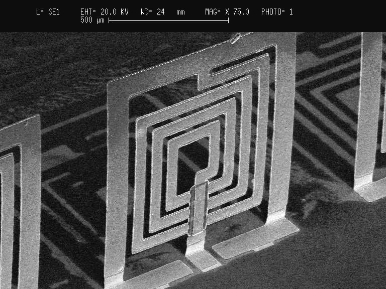
Transcription
1 MEMS for RF, Micro Optics and Scanning Probe Nanotechnology Applications
2 Part I: RF Applications Introductions and Motivations What are RF MEMS? Example Devices


3 RFIC RFIC consists of Active components Transistors and diodes High level of integration Passive components Capacitors, inductors, waveguides, antenna and filters Discrete components used
 Monolithic integration with active components Small")

4 Toward Higher Level of Integration The major possible contribution of MEMS in RF IC is to enable new types of RF passive components (RF MEMS) Monolithic integration with active components Small size and highly functional (e.g. tunable) Higher performance (e.g. higher quality factor and lower loss) Reducing the number of discrete components and the cost of packaging (enhancing the reliability)
5 Typical RF MEMS devices Tunable capacitors vs. (PN junction and MOS capacitor) Advantages: much wider tuning range (DC/C), lower loss, insensitive to RF interference Challenges: high driving voltage, slow tuning speed (10 s µs) Inductors Advantages: much higher quality factor and also inductance Challenges: more complex fabrication and integration process Switches and relays vs. (PIN diodes) Advantages: much higher ON/OFF ratio and lower loss Challenges: high driving voltage, slow switching speed, reliability Resonators vs. Quartz resonators Advantages: Integrated and comparable quality factor Challenges: stability and reliability

6 On-chip (integrated) Inductors Electromagnetic coupling causing loss and parasitics 1 st Metal 2 nd Metal layer layer SiO 2 Si On-chip inductors are one of the major performance-limiting passive components in current RF ICs. Low quality factor due to substrate loss and parasitics (Q<20) Q should be as high as possible Large footprint (100s 100smm 2 )
7 Micromachined Spiral Inductors Polyimide Air Gap Si Applying a thick polyimide layer underneath Glass Levitating the inductor structure above the substrate Si Si Completely removing substrate material underneath Si Partially removing substrate material underneath Still Large footprint Involving complex microfabrication steps, possibly not compatible with IC fabrication


8 A 3D Solution Fabricate inductor on IC substrates Integrated circuits Put the spiral inductor into vertical position Reduce substrate loss and parasitics Higher Q Zero footprint But how?

9 The Prototype PDMA

10 Typical Electrostatic Actuated RF MEMS Switches: Capacitive ON State OFF State Co-planar waveguide (CPW) configuration ON state: C off = 25~50fF OFF state: C on = 3~4pF (serving as a short between the signal line and the ground line. Driving voltage larger than pull-in voltage

11 Typical Electrostatic Actuated RF MEMS Switches: Contact Co-planar waveguide (CPW) configuration Issue related the operation of the contact RF MEMS switch Stress in the gold films The contact point could fatigue and wear after continuous operation.
 Difficult to integrate Developing MEMS resonators for integrated, high quality factor filters based on the")
12 MEMS Resonators Current electronic filters used in RFICs RLC filters based on electrical resonance Low quality factor and frequency selectivity Difficult to integrate Filters using quartz based on mechanical resonance of the piezoelectric quartz crystal High quality factor (30,000) Difficult to integrate Developing MEMS resonators for integrated, high quality factor filters based on the resonance of micromechanical structures. electrical input signal Mechanical vibration and resonance Filtered electrical output signal

13 MEMS Resonators The input voltage causes the left comb drive (longitudinal or transverse?) to vibrate. The amplitude of the vibration depends on the frequency of the input signal and it will reach the maximum at the resonant frequency of the entire movable comb drive structure. The vibration cause the capacitance within the right comb drive to change, which can read out at the output. Frequency: 1~100kHz, Quality factor: ~8000 (in air or in vacuum?) The driving and signal read-out do not have to be electrostatic.
14 Part II: Micro Optics Applications
15 Introduction MEMS applications in optics Phase correction Pattern generation and projection Switching and scanning of optical beams

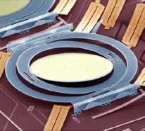
16 Adaptive Optical MEMS Devices Transitional mirrors Adjust the travel distance of light Deflection of rigid plates Piston motion membranes


17 Adaptive Optical MEMS Devices Deformable micro mirror array Piston motion micro mirror array Micromachined deformable mirror array

18 Rotational Scanning Mirrors Bent cantilever beams Top surface serves as reflector Mirror surface supported by torsional structures Able to generate large angles with reasonable actuation force


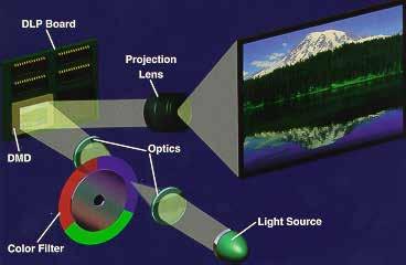
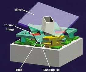
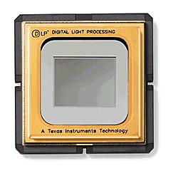
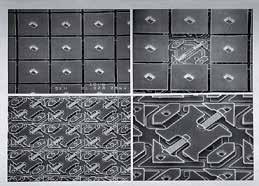
19 Digital Mirror Device +/-10 o

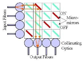
20 MEMS Optical Switches


21 Rotational Scanning Mirrors


22 Endoscopic Probe with Micromotor: 3D Helix Scan Rabbit esophagus Specifics Outer diameter: 2.7 mm Motor diameter: ~2.0mm with cycle feedback control Rigid length: 2.5 cm Liner transversal stage pulling of flexible part J. P. Su, Optical Express, 15, 16, 10390, 2007 Rabbit trachea
23 Part III: Scanning Probe Application Introduction and Motivation Dip-pen Nanolithography Examples of Application 1-D passive scanning probe array 1-D active scanning probe array 2-D active scanning probe array

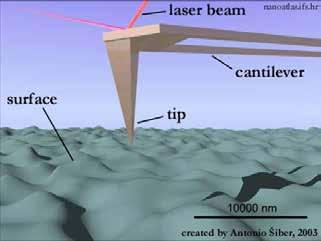
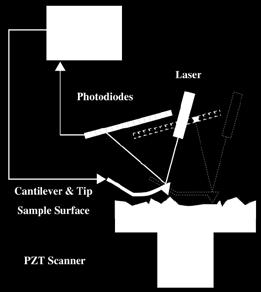

24 Scanning Probe Microscopy Atomic force microscope

25 Scanning Probe Array
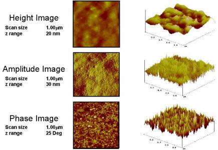
 Suitable for both bottom-up and top-down approaches LFM images of 1-octadecanethiol (ODT) patterns by DPN (60nm)")
26 Dip-Pen Nanolithography The process Utilize a sharp scanning probe Coat the probe tip with ink Contact sample surface and form water meniscus Scan (using AFM machine) The advantages Nanometer resolution Direct patterning, no mask and photoresist involved Compatible with a wide range of chemicals (e.g. bio-chemicals) Suitable for both bottom-up and top-down approaches LFM images of 1-octadecanethiol (ODT) patterns by DPN (60nm)
27 Scanning Probe Array for DPN To develop large DPN probe arrays to increase the writing speed. Passive probe array A A A A A A A A Duplicate identical features Passive probe array A B C D E F G H Each probe has a micro actuator and is individually addressable. Flexibility for complex features


28 1D Passive DPN Probe Arrays Silicon nitride probe array Duplicate identical features Silicon probe array p++ doped layer


29 1D Active SiN DPN Probe Arrays Gold * David Bullen, et al, "Design, Fabrication, and Characterization of Thermally Actuated Probe Arrays for Dip Pen Nanolithography," JMEMS, 2004.

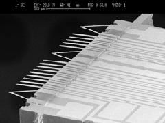
30 2D Active Probe Array 7 7 array packaged on a micromachined silicon chip holder

31 2D Active Probe Array Probe chip SiN Gold Writing sample Bimetallic Thermal Actuator

32 Actuation of 2D Active Probe Array Microscope Cool down Heat up Gold Si Nitride

33 Experimental Result 150nm LFM images of ODT patterns written simultaneously by the scanning probe array
MEMS in ECE at CMU. Gary K. Fedder
 MEMS in ECE at CMU Gary K. Fedder Department of Electrical and Computer Engineering and The Robotics Institute Carnegie Mellon University Pittsburgh, PA 15213-3890 fedder@ece.cmu.edu http://www.ece.cmu.edu/~mems
DEVELOPMENT OF RF MEMS SYSTEMS
 DEVELOPMENT OF RF MEMS SYSTEMS Ivan Puchades, Ph.D. Research Assistant Professor Electrical and Microelectronic Engineering Kate Gleason College of Engineering Rochester Institute of Technology 82 Lomb
Introduction to Microeletromechanical Systems (MEMS) Lecture 12 Topics. MEMS Overview
 Lecture 12 Topics. MEMS Overview") Introduction to Microeletromechanical Systems (MEMS) Lecture 2 Topics MEMS for Wireless Communication Components for Wireless Communication Mechanical/Electrical Systems Mechanical Resonators o Quality
Introduction to Microeletromechanical Systems (MEMS) Lecture 2 Topics MEMS for Wireless Communication Components for Wireless Communication Mechanical/Electrical Systems Mechanical Resonators o Quality
- Near Field Scanning Optical Microscopy - Electrostatic Force Microscopy - Magnetic Force Microscopy
 - Near Field Scanning Optical Microscopy - Electrostatic Force Microscopy - Magnetic Force Microscopy Yongho Seo Near-field Photonics Group Leader Wonho Jhe Director School of Physics and Center for Near-field
Micro-nanosystems for electrical metrology and precision instrumentation
 Micro-nanosystems for electrical metrology and precision instrumentation A. Bounouh 1, F. Blard 1,2, H. Camon 2, D. Bélières 1, F. Ziadé 1 1 LNE 29 avenue Roger Hennequin, 78197 Trappes, France, alexandre.bounouh@lne.fr
MICROMACHINED INTERFEROMETER FOR MEMS METROLOGY
 MICROMACHINED INTERFEROMETER FOR MEMS METROLOGY Byungki Kim, H. Ali Razavi, F. Levent Degertekin, Thomas R. Kurfess G.W. Woodruff School of Mechanical Engineering, Georgia Institute of Technology, Atlanta,
RF MEMS for Low-Power Communications
 RF MEMS for Low-Power Communications Clark T.-C. Nguyen Center for Wireless Integrated Microsystems Dept. of Electrical Engineering and Computer Science University of Michigan Ann Arbor, Michigan 48109-2122
High Power RF MEMS Switch Technology
 High Power RF MEMS Switch Technology Invited Talk at 2005 SBMO/IEEE MTT-S International Conference on Microwave and Optoelectronics Conference Dr Jia-Sheng Hong Heriot-Watt University Edinburgh U.K. 1
RF MEMS Simulation High Isolation CPW Shunt Switches
 RF MEMS Simulation High Isolation CPW Shunt Switches Authored by: Desmond Tan James Chow Ansoft Corporation Ansoft 2003 / Global Seminars: Delivering Performance Presentation #4 What s MEMS Micro-Electro-Mechanical
Micro-sensors - what happens when you make "classical" devices "small": MEMS devices and integrated bolometric IR detectors
 Micro-sensors - what happens when you make "classical" devices "small": MEMS devices and integrated bolometric IR detectors Dean P. Neikirk 1 MURI bio-ir sensors kick-off 6/16/98 Where are the targets
INF 5490 RF MEMS. LN12: RF MEMS inductors. Spring 2011, Oddvar Søråsen Department of informatics, UoO
 INF 5490 RF MEMS LN12: RF MEMS inductors Spring 2011, Oddvar Søråsen Department of informatics, UoO 1 Today s lecture What is an inductor? MEMS -implemented inductors Modeling Different types of RF MEMS
Piezoelectric Sensors and Actuators
 Piezoelectric Sensors and Actuators Outline Piezoelectricity Origin Polarization and depolarization Mathematical expression of piezoelectricity Piezoelectric coefficient matrix Cantilever piezoelectric
Surface Micromachining
 Surface Micromachining An IC-Compatible Sensor Technology Bernhard E. Boser Berkeley Sensor & Actuator Center Dept. of Electrical Engineering and Computer Sciences University of California, Berkeley Sensor
Lecture 20: Optical Tools for MEMS Imaging
 MECH 466 Microelectromechanical Systems University of Victoria Dept. of Mechanical Engineering Lecture 20: Optical Tools for MEMS Imaging 1 Overview Optical Microscopes Video Microscopes Scanning Electron
Fabrication and application of a wireless inductance-capacitance coupling microsensor with electroplated high permeability material NiFe
 Journal of Physics: Conference Series Fabrication and application of a wireless inductance-capacitance coupling microsensor with electroplated high permeability material NiFe To cite this article: Y H
Manufacturing Development of a New Electroplated Magnetic Alloy Enabling Commercialization of PwrSoC Products
 Manufacturing Development of a New Electroplated Magnetic Alloy Enabling Commercialization of PwrSoC Products Trifon Liakopoulos, Amrit Panda, Matt Wilkowski and Ashraf Lotfi PowerSoC 2012 CONTENTS Definitions
attosnom I: Topography and Force Images NANOSCOPY APPLICATION NOTE M06 RELATED PRODUCTS G
 APPLICATION NOTE M06 attosnom I: Topography and Force Images Scanning near-field optical microscopy is the outstanding technique to simultaneously measure the topography and the optical contrast of a sample.
Waveguide-Mounted RF MEMS for Tunable W-band Analog Type Phase Shifter
 Waveguide-Mounted RF MEMS for Tunable W-band Analog Type Phase Shifter D. PSYCHOGIOU 1, J. HESSELBARTH 1, Y. LI 2, S. KÜHNE 2, C. HIEROLD 2 1 Laboratory for Electromagnetic Fields and Microwave Electronics
SENSOR+TEST Conference SENSOR 2009 Proceedings II
 B8.4 Optical 3D Measurement of Micro Structures Ettemeyer, Andreas; Marxer, Michael; Keferstein, Claus NTB Interstaatliche Hochschule für Technik Buchs Werdenbergstr. 4, 8471 Buchs, Switzerland Introduction
A large-area wireless power transmission sheet using printed organic. transistors and plastic MEMS switches
 Supplementary Information A large-area wireless power transmission sheet using printed organic transistors and plastic MEMS switches Tsuyoshi Sekitani 1, Makoto Takamiya 2, Yoshiaki Noguchi 1, Shintaro
Conference Paper Cantilever Beam Metal-Contact MEMS Switch
 Conference Papers in Engineering Volume 2013, Article ID 265709, 4 pages http://dx.doi.org/10.1155/2013/265709 Conference Paper Cantilever Beam Metal-Contact MEMS Switch Adel Saad Emhemmed and Abdulmagid
BMC s heritage deformable mirror technology that uses hysteresis free electrostatic
 Optical Modulator Technical Whitepaper MEMS Optical Modulator Technology Overview The BMC MEMS Optical Modulator, shown in Figure 1, was designed for use in free space optical communication systems. The
Low Actuation Wideband RF MEMS Shunt Capacitive Switch
 Available online at www.sciencedirect.com Procedia Engineering 29 (2012) 1292 1297 2012 International Workshop on Information and Electronics Engineering (IWIEE) Low Actuation Wideband RF MEMS Shunt Capacitive
Figure 1: Layout of the AVC scanning micromirror including layer structure and comb-offset view
 Bauer, Ralf R. and Brown, Gordon G. and Lì, Lì L. and Uttamchandani, Deepak G. (2013) A novel continuously variable angular vertical combdrive with application in scanning micromirror. In: 2013 IEEE 26th
Vibrating MEMS resonators
 Vibrating MEMS resonators Vibrating resonators can be scaled down to micrometer lengths Analogy with IC-technology Reduced dimensions give mass reduction and increased spring constant increased resonance
Body-Biased Complementary Logic Implemented Using AlN Piezoelectric MEMS Switches
 University of Pennsylvania From the SelectedWorks of Nipun Sinha 29 Body-Biased Complementary Logic Implemented Using AlN Piezoelectric MEMS Switches Nipun Sinha, University of Pennsylvania Timothy S.
Cutting-edge Atomic Force Microscopy techniques for large and multiple samples
 Cutting-edge Atomic Force Microscopy techniques for large and multiple samples Study of up to 200 mm samples using the widest set of AFM modes Industrial standards of automation A unique combination of
A Review of MEMS Based Piezoelectric Energy Harvester for Low Frequency Applications
 Available Online at www.ijcsmc.com International Journal of Computer Science and Mobile Computing A Monthly Journal of Computer Science and Information Technology IJCSMC, Vol. 3, Issue. 9, September 2014,
Electrostatically Tunable Analog Single Crystal Silicon Fringing-Field MEMS Varactors
 Purdue University Purdue e-pubs Birck and NCN Publications Birck Nanotechnology Center 2009 Electrostatically Tunable Analog Single Crystal Silicon Fringing-Field MEMS Varactors Joshua A. Small Purdue
Measurement of Microscopic Three-dimensional Profiles with High Accuracy and Simple Operation
 238 Hitachi Review Vol. 65 (2016), No. 7 Featured Articles Measurement of Microscopic Three-dimensional Profiles with High Accuracy and Simple Operation AFM5500M Scanning Probe Microscope Satoshi Hasumura
Akiyama-Probe (A-Probe) guide
 guide") Akiyama-Probe (A-Probe) guide This guide presents: what is Akiyama-Probe, how it works, and what you can do Dynamic mode AFM Version: 2.0 Introduction NANOSENSORS Akiyama-Probe (A-Probe) is a self-sensing
Akiyama-Probe (A-Probe) guide This guide presents: what is Akiyama-Probe, how it works, and what you can do Dynamic mode AFM Version: 2.0 Introduction NANOSENSORS Akiyama-Probe (A-Probe) is a self-sensing
INDIAN INSTITUTE OF TECHNOLOGY BOMBAY
 IIT Bombay requests quotations for a high frequency conducting-atomic Force Microscope (c-afm) instrument to be set up as a Central Facility for a wide range of experimental requirements. The instrument
Akiyama-Probe (A-Probe) guide
 guide") Akiyama-Probe (A-Probe) guide This guide presents: what is Akiyama-Probe, how it works, and its performance. Akiyama-Probe is a patented technology. Version: 2009-03-23 Introduction NANOSENSORS Akiyama-Probe
Akiyama-Probe (A-Probe) guide This guide presents: what is Akiyama-Probe, how it works, and its performance. Akiyama-Probe is a patented technology. Version: 2009-03-23 Introduction NANOSENSORS Akiyama-Probe
Deformable Membrane Mirror for Wavefront Correction
 Defence Science Journal, Vol. 59, No. 6, November 2009, pp. 590-594 Ó 2009, DESIDOC SHORT COMMUNICATION Deformable Membrane Mirror for Wavefront Correction Amita Gupta, Shailesh Kumar, Ranvir Singh, Monika
Nanostencil Lithography and Nanoelectronic Applications
 Microsystems Laboratory Nanostencil Lithography and Nanoelectronic Applications Oscar Vazquez, Marc van den Boogaart, Dr. Lianne Doeswijk, Prof. Juergen Brugger, LMIS1 Dr. Chan Woo Park, Visiting Professor
Akiyama-Probe (A-Probe) technical guide This technical guide presents: how to make a proper setup for operation of Akiyama-Probe.
 technical guide This technical guide presents: how to make a proper setup for operation of Akiyama-Probe.") Akiyama-Probe (A-Probe) technical guide This technical guide presents: how to make a proper setup for operation of Akiyama-Probe. Version: 2.0 Introduction To benefit from the advantages of Akiyama-Probe,
Akiyama-Probe (A-Probe) technical guide This technical guide presents: how to make a proper setup for operation of Akiyama-Probe. Version: 2.0 Introduction To benefit from the advantages of Akiyama-Probe,
3-5μm F-P Tunable Filter Array based on MEMS technology
 Journal of Physics: Conference Series 3-5μm F-P Tunable Filter Array based on MEMS technology To cite this article: Wei Xu et al 2011 J. Phys.: Conf. Ser. 276 012052 View the article online for updates
College of Engineering Department of Electrical Engineering and Computer Sciences University of California, Berkeley
 College of Engineering Department of Electrical Engineering and Below are your weekly quizzes. You should print out a copy of the quiz and complete it before your lab section. Bring in the completed quiz
USER MANUAL VarioS-Microscanner-Demonstrators
 FRAUNHOFER INSTITUTE FOR PHOTONIC MICROSYSTEMS IPMS USER MANUAL VarioS-Microscanner-Demonstrators last revision : 2014-11-14 [Fb046.08] USER MANUAL.doc Introduction Thank you for purchasing a VarioS-microscanner-demonstrator
Design and Fabrication of RF MEMS Switch by the CMOS Process
 Tamkang Journal of Science and Engineering, Vol. 8, No 3, pp. 197 202 (2005) 197 Design and Fabrication of RF MEMS Switch by the CMOS Process Ching-Liang Dai 1 *, Hsuan-Jung Peng 1, Mao-Chen Liu 1, Chyan-Chyi
Large-scale metal MEMS mirror arrays with integrated
 Large-scale metal MEMS mirror arrays with integrated electronics Thomas Bifano', Paul Bierden2, Steven Cornelissen1, Clara Dimas2, Hocheol Lee1, Michele Miller3, and Julie Perreault1 'Boston University,
An X band RF MEMS switch based on silicon-on-glass architecture
 Sādhanā Vol. 34, Part 4, August 2009, pp. 625 631. Printed in India An X band RF MEMS switch based on silicon-on-glass architecture M S GIRIDHAR, ASHWINI JAMBHALIKAR, J JOHN, R ISLAM, C L NAGENDRA and
High-speed wavefront control using MEMS micromirrors T. G. Bifano and J. B. Stewart, Boston University [ ] Introduction
![High-speed wavefront control using MEMS micromirrors T. G. Bifano and J. B. Stewart, Boston University [ ] Introduction](/thumbs/72/66548311.jpg "High-speed wavefront control using MEMS micromirrors T. G. Bifano and J. B. Stewart, Boston University [ ] Introduction") High-speed wavefront control using MEMS micromirrors T. G. Bifano and J. B. Stewart, Boston University [5895-27] Introduction Various deformable mirrors for high-speed wavefront control have been demonstrated
High-speed wavefront control using MEMS micromirrors T. G. Bifano and J. B. Stewart, Boston University [5895-27] Introduction Various deformable mirrors for high-speed wavefront control have been demonstrated
Magnetic and Electromagnetic Microsystems. 4. Example: magnetic read/write head
 Magnetic and Electromagnetic Microsystems 1. Magnetic Sensors 2. Magnetic Actuators 3. Electromagnetic Sensors 4. Example: magnetic read/write head (C) Andrei Sazonov 2005, 2006 1 Magnetic microsystems
Modal Analysis of Microcantilever using Vibration Speaker
 Modal Analysis of Microcantilever using Vibration Speaker M SATTHIYARAJU* 1, T RAMESH 2 1 Research Scholar, 2 Assistant Professor Department of Mechanical Engineering, National Institute of Technology,
Micromachined Switches and Relays
 Micromachined Switches and Relays Micro Actuators, Sensors, Systems Group University of Illinois at Urbana-Champaign Outline Motivation Relays: for low frequency signals Switches: for low and high frequency
MEMS Technologies and Devices for Single-Chip RF Front-Ends
 MEMS Technologies and Devices for Single-Chip RF Front-Ends Clark T.-C. Nguyen Dept. of Electrical Engineering & Computer Science University of Michigan Ann Arbor, Michigan 48105-2122 CCMT 06 April 25,
Adaptive Focal Plane Array - A Compact Spectral Imaging Sensor
 Adaptive Focal Plane Array - A Compact Spectral Imaging Sensor William Gunning March 5 2007 Report Documentation Page Form Approved OMB No. 0704-0188 Public reporting burden for the collection of information
AFM of High-Profile Surfaces
 AFM of High-Profile Surfaces Fig. 1. AFM topograpgy image of black Si made using SCD probe tip. Scan size 4. Profile height is more than 8. See details and other application examples below. High Aspect
CONTENTS. Foreword S. D. Senturia. M. E. Motamedi Acknowledgments
 CONTENTS Foreword S. D. Senturia Preface M. E. Motamedi Acknowledgments xv xvii xix 1 Introduction 1 M. E. Motamedi 1.1 Integrated circuits and the evolution of micromachining 1 1.2 MEMS review 3 1.3 New
NOISE IN MEMS PIEZORESISTIVE CANTILEVER
 NOISE IN MEMS PIEZORESISTIVE CANTILEVER Udit Narayan Bera Mechatronics, IIITDM Jabalpur, (India) ABSTRACT Though pezoresistive cantilevers are very popular for various reasons, they are prone to noise
Dry release fabrication and testing of SiC electrostatic cantilever actuators
 Microelectronic Engineering 78 79 (5) 16 111 www.elsevier.com/locate/mee Dry release fabrication and testing of SiC electrostatic cantilever actuators Liudi Jiang a, *, M. Hassan b, R. Cheung a, A.J. Harris
Vibrating RF MEMS for Low Power Wireless Communications
 Vibrating RF MEMS for Low Power Wireless Communications Clark T.-C. Nguyen Center for Wireless Integrated Microsystems Dept. of Electrical Engineering and Computer Science University of Michigan Ann Arbor,
RF(Radio Frequency) MEMS (Micro Electro Mechanical
 MEMS (Micro Electro Mechanical") Design and Analysis of Piezoelectrically Actuated RF-MEMS Switches using PZT and AlN PrashantTippimath M.Tech., Scholar, Dept of ECE M.S.Ramaiah Institute of Technology Bengaluru tippimathprashant@gmail.com
Design and Analysis of Piezoelectrically Actuated RF-MEMS Switches using PZT and AlN PrashantTippimath M.Tech., Scholar, Dept of ECE M.S.Ramaiah Institute of Technology Bengaluru tippimathprashant@gmail.com
Vertical Integration of MM-wave MMIC s and MEMS Antennas
 JOURNAL OF SEMICONDUCTOR TECHNOLOGY AND SCIENCE, VOL.6, NO.3, SEPTEMBER, 2006 169 Vertical Integration of MM-wave MMIC s and MEMS Antennas Youngwoo Kwon, Yong-Kweon Kim, Sanghyo Lee, and Jung-Mu Kim Abstract
Micromechanical Circuits for Wireless Communications
 Micromechanical Circuits for Wireless Communications Clark T.-C. Nguyen Center for Integrated Microsystems Dept. of Electrical Engineering and Computer Science University of Michigan Ann Arbor, Michigan
CHAPTER 2 RF MEMS BASICS. 2.1 Switches for Microwave Applications
 CHAPTER 2 RF MEMS BASICS This chapter provides the basic introduction to RF MEMS switches. RF MEMS have in general seen a remarkable growth in the past two decades due to the immense potentials in defense
Basic methods in imaging of micro and nano structures with atomic force microscopy (AFM)
") Basic methods in imaging of micro and nano P2538000 AFM Theory The basic principle of AFM is very simple. The AFM detects the force interaction between a sample and a very tiny tip (
Basic methods in imaging of micro and nano P2538000 AFM Theory The basic principle of AFM is very simple. The AFM detects the force interaction between a sample and a very tiny tip (
PRINCIPLES OF RADAR. By Members of the Staff of the Radar School Massachusetts Institute of Technology. Third Edition by J.
 PRINCIPLES OF RADAR By Members of the Staff of the Radar School Massachusetts Institute of Technology Third Edition by J. Francis Reintjes ASSISTANT PBOFESSOR OF COMMUNICATIONS MASSACHUSETTS INSTITUTE
Special Lecture Series Biosensors and Instrumentation
 !1 Special Lecture Series Biosensors and Instrumentation Lecture 6: Micromechanical Sensors 1 This is the first part of the material on micromechanical sensors which deals with piezoresistive and piezoelectric
Micro- and nano-scale switches and tuning elements for microwave applications
 University of South Florida Scholar Commons Graduate Theses and Dissertations Graduate School 26 Micro- and nano-scale switches and tuning elements for microwave applications Thomas P. Ketterl University
 Distributed by: www.jameco.com -800-83-4242 The content and copyrights of the attached material are the property of its owner. HPND- 4005 Beam Lead PIN Diode Data Sheet Description The HPND-4005 planar
Study of MEMS Devices for Space Applications ~Study Status and Subject of RF-MEMS~
 Study of MEMS Devices for Space Applications ~Study Status and Subject of RF-MEMS~ The 26 th Microelectronics Workshop October, 2013 Maya Kato Electronic Devices and Materials Group Japan Aerospace Exploration
On-chip 3D air core micro-inductor for high-frequency applications using deformation of sacrificial polymer
 header for SPIE use On-chip 3D air core micro-inductor for high-frequency applications using deformation of sacrificial polymer Nimit Chomnawang and Jeong-Bong Lee Department of Electrical and Computer
Atomic Force Microscopy (Bruker MultiMode Nanoscope IIIA)
") Atomic Force Microscopy (Bruker MultiMode Nanoscope IIIA) This operating procedure intends to provide guidance for general measurements with the AFM. For more advanced measurements or measurements with
Atomic Force Microscopy (Bruker MultiMode Nanoscope IIIA) This operating procedure intends to provide guidance for general measurements with the AFM. For more advanced measurements or measurements with
Academic Course Description SRM University Faculty of Engineering and Technology Department of Electronics and Communication Engineering
 Academic Course Description SRM University Faculty of Engineering and Technology Department of Electronics and Communication Engineering EC0032 Introduction to MEMS Eighth semester, 2014-15 (Even Semester)
Smart Antenna using MTM-MEMS
 Smart Antenna using MTM-MEMS Georgina Rosas a, Roberto Murphy a, Wilfrido Moreno b a Department of Electronics, National Institute of Astrophysics, Optics and Electronics, 72840, Puebla, MEXICO b Department
IST IP NOBEL "Next generation Optical network for Broadband European Leadership"
 DBR Tunable Lasers A variation of the DFB laser is the distributed Bragg reflector (DBR) laser. It operates in a similar manner except that the grating, instead of being etched into the gain medium, is
Micro- & Nano-technologies pour applications hyperfréquence à Thales Research &Technology Afshin Ziaei, Sébastien Demoustier, Eric Minoux
 Micro- & Nano-technologies pour applications hyperfréquence à Thales Research &Technology Afshin Ziaei, Sébastien Demoustier, Eric Minoux Outline Application hyperfréquence à THALES: Antenne à réseau réflecteur
Catalog Continuing Education Courses
 Catalog Continuing Education Courses NanoMEMS Research, LLC P.O. Box 18614 Irvine, CA 92623-8614 Tel.: (949)682-7702 URL: www.nanomems-research.com E-mail: info@nanomems-research.com 2011 NanoMEMS Research,
Silicon Light Machines Patents
 820 Kifer Road, Sunnyvale, CA 94086 Tel. 408-240-4700 Fax 408-456-0708 www.siliconlight.com Silicon Light Machines Patents USPTO No. US 5,808,797 US 5,841,579 US 5,798,743 US 5,661,592 US 5,629,801 US
Characterization of Silicon-based Ultrasonic Nozzles
 Tamkang Journal of Science and Engineering, Vol. 7, No. 2, pp. 123 127 (24) 123 Characterization of licon-based Ultrasonic Nozzles Y. L. Song 1,2 *, S. C. Tsai 1,3, Y. F. Chou 4, W. J. Chen 1, T. K. Tseng
Integrated diodes. The forward voltage drop only slightly depends on the forward current. ELEKTRONIKOS ĮTAISAI
 1 Integrated diodes pn junctions of transistor structures can be used as integrated diodes. The choice of the junction is limited by the considerations of switching speed and breakdown voltage. The forward
MEMS Technologies for Communications
 MEMS Technologies for Communications Clark T.-C. Nguyen Program Manager, MPG/CSAC/MX Microsystems Technology Office () Defense Advanced Research Projects Agency Nanotech 03 Feb. 25, 2003 Outline Introduction:
Out-of-plane translatory MEMS actuator with extraordinary large stroke for optical path length modulation in miniaturized FTIR spectrometers
 P 12 Out-of-plane translatory MEMS actuator with extraordinary large stroke for optical path length modulation in miniaturized FTIR spectrometers Sandner, Thilo; Grasshoff, Thomas; Schenk, Harald; Kenda*,
Outline: Introduction: What is SPM, history STM AFM Image treatment Advanced SPM techniques Applications in semiconductor research and industry
 1 Outline: Introduction: What is SPM, history STM AFM Image treatment Advanced SPM techniques Applications in semiconductor research and industry 2 Back to our solutions: The main problem: How to get nm
EE C245 ME C218 Introduction to MEMS Design
 EE C245 ME C218 Introduction to MEMS Design Fall 2008 Prof. Clark T.-C. Nguyen Dept. of Electrical Engineering & Computer Sciences University of California at Berkeley Berkeley, CA 94720 Lecture 1: Definition
Design of MEMS Tunable Inductor Implemented on SOI and Glass wafers Using Bonding Technology
 Design of MEMS Tunable Inductor Implemented on SOI and Glass wafers Using Bonding Technology USAMA ZAGHLOUL* AMAL ZAKI* HAMED ELSIMARY* HANI GHALI** and HANI FIKRI** * Electronics Research Institute, **
NSOM (SNOM) Overview
 Overview") NSOM (SNOM) Overview The limits of far field imaging In the early 1870s, Ernst Abbe formulated a rigorous criterion for being able to resolve two objects in a light microscope: d > ë / (2sinè) where d
NSOM (SNOM) Overview The limits of far field imaging In the early 1870s, Ernst Abbe formulated a rigorous criterion for being able to resolve two objects in a light microscope: d > ë / (2sinè) where d
Design of Metal MUMPs based LLC Resonant Converter for On-chip Power Supplies
 Design of Metal MUMPs based LLC Resonant Converter for On-chip Power Supplies Fahimullah Khan, a, Yong Zhu,, b Junwei Lu,,c,Dzung Dao,,d Queensland Micro & Nanotechnology Centre Griffith University, Nathan,
LAB UNIT 1: Introduction Scanning Force Microscopy
 LAB UNIT 1: Introduction Specific Assignment: Setup of scanning force microscopy experiment and first contact measurements Objective Outcome Synopsis The student will become familiar with contact mode
2D Asymmetric Silicon Micro-Mirrors for Ranging Measurements
 D Asymmetric Silicon Micro-Mirrors for Ranging Measurements Takaki Itoh * (Industrial Technology Center of Wakayama Prefecture) Toshihide Kuriyama (Kinki University) Toshiyuki Nakaie,Jun Matsui,Yoshiaki
MEMS Processes at CMP
 MEMS Processes at CMP MEMS Processes Bulk Micromachining MUMPs from MEMSCAP Teledyne DALSA MIDIS Micralyne MicraGEM-Si CEA/LETI Photonic Si-310 PHMP2M 2 Bulk micromachining on CMOS Compatible with electronics
A Novel Electromechanical Interrogation Scheme for Implantable Passive Transponders
 Purdue University Purdue e-pubs Birck and NCN Publications Birck Nanotechnology Center 1-29-212 A Novel Electromechanical Interrogation Scheme for Implantable Passive Transponders Albert Kim Birck Nanotechnology
RF MEMS Circuits Applications of MEMS switch and tunable capacitor
 RF MEMS Circuits Applications of MEMS switch and tunable capacitor Dr. Jeffrey DeNatale, Manager, MEMS Department Electronics Division jdenatale@rwsc.com 85-373-4439 Panamerican Advanced Studies Institute
INF5490 RF MEMS. L7: RF MEMS switches, I. S2008, Oddvar Søråsen Department of Informatics, UoO
 INF5490 RF MEMS L7: RF MEMS switches, I S2008, Oddvar Søråsen Department of Informatics, UoO 1 Today s lecture Switches for RF and microwave Examples Performance requirements Technology Characteristics
Novel piezoresistive e-nose sensor array cell
 4M2007 Conference on Multi-Material Micro Manufacture 3-5 October 2007 Borovets Bulgaria Novel piezoresistive e-nose sensor array cell V.Stavrov a, P.Vitanov b, E.Tomerov a, E.Goranova b, G.Stavreva a
EE C245 ME C218 Introduction to MEMS Design Fall 2010
 Instructor: Prof. Clark T.-C. Nguyen EE C245 ME C218 Introduction to MEMS Design Fall 2010 Prof. Clark T.-C. Nguyen Dept. of Electrical Engineering & Computer Sciences University of California at Berkeley
Characteristics of Crystal. Piezoelectric effect of Quartz Crystal
 Characteristics of Crystal Piezoelectric effect of Quartz Crystal The quartz crystal has a character when the pressure is applied to the direction of the crystal axis, the electric change generates on
Industrialization of Micro-Electro-Mechanical Systems. Werner Weber Infineon Technologies
 Industrialization of Micro-Electro-Mechanical Systems Werner Weber Infineon Technologies Semiconductor-based MEMS market MEMS Market 2004 (total 22.7 BUS$) Others mostly Digital Light Projection IR Sensors
Indentation Cantilevers
 curve is recorded utilizing the DC displacement of the cantilever versus the extension of the scanner. Many indentations may be made using various forces, rates, etc. Upon exiting indentation mode, TappingMode
Interdigital Bandpass Filter Using capacitive RF MEMS Switches
 Interdigital Bandpass Filter Using capacitive RF MEMS Switches D.Pooja 1, C.Selvi 2 P.G. Student, Department of Communication Systems, Muthayammal Engineering College, Rasipuram, Namakkal, Tamilnadu, India.
Sensitivity Enhancement of Bimaterial MOEMS Thermal Imaging Sensor Array using 2-λ readout
 Sensitivity Enhancement of Bimaterial MOEMS Thermal Imaging Sensor Array using -λ readout O. Ferhanoğlu, H. Urey Koç University, Electrical Engineering, Istanbul-TURKEY ABSTRACT Diffraction gratings integrated
Advanced RF MEMS CAMBRIDGE UNIVERSITY PRESS. Edited by STEPAN LUCYSZYN. Imperial College London
 Advanced RF MEMS Edited by STEPAN LUCYSZYN Imperial College London n CAMBRIDGE UNIVERSITY PRESS Contents List of contributors Preface List of abbreviations page xiv xvii xx Introduction 1 1.1 Introduction
High-yield Fabrication Methods for MEMS Tilt Mirror Array for Optical Switches
 : MEMS Device Technologies High-yield Fabrication Methods for MEMS Tilt Mirror Array for Optical Switches Joji Yamaguchi, Tomomi Sakata, Nobuhiro Shimoyama, Hiromu Ishii, Fusao Shimokawa, and Tsuyoshi
Optical Bus for Intra and Inter-chip Optical Interconnects
 Optical Bus for Intra and Inter-chip Optical Interconnects Xiaolong Wang Omega Optics Inc., Austin, TX Ray T. Chen University of Texas at Austin, Austin, TX Outline Perspective of Optical Backplane Bus
77 GHz VCO for Car Radar Systems T625_VCO2_W Preliminary Data Sheet
 77 GHz VCO for Car Radar Systems Preliminary Data Sheet Operating Frequency: 76-77 GHz Tuning Range > 1 GHz Output matched to 50 Ω Application in Car Radar Systems ESD: Electrostatic discharge sensitive
Final Exam Topics. IC Technology Advancement. Microelectronics Technology in the 21 st Century. Intel s 90 nm CMOS Technology. 14 nm CMOS Transistors
 ANNOUNCEMENTS Final Exam: When: Wednesday 12/10 12:30-3:30PM Where: 10 Evans (last names beginning A-R) 60 Evans (last names beginning S-Z) Comprehensive coverage of course material Closed book; 3 sheets
SMART SENSOR SYSTEMS. WILEY A John Wiley and Sons, Ltd, Publication. Edited by. Gerard CM. Meijer
 SMART SENSOR SYSTEMS Edited by Gerard CM. Meijer Delft University of Technology, the Netherlands SensArt, Delft, the Netherlands WILEY A John Wiley and Sons, Ltd, Publication Preface About the Authors
UNIVERSITY OF WATERLOO Physics 360/460 Experiment #2 ATOMIC FORCE MICROSCOPY
 UNIVERSITY OF WATERLOO Physics 360/460 Experiment #2 ATOMIC FORCE MICROSCOPY References: http://virlab.virginia.edu/vl/home.htm (University of Virginia virtual lab. Click on the AFM link) An atomic force