Recent Developments in Multifunctional Integration. Stephan Guttowski, Head of Technology Park»Heterointegration«, Fraunhofer FMD
|
|
|
- Sybil Riley
- 5 years ago
- Views:
Transcription

1 Recent Developments in Multifunctional Integration Stephan Guttowski, Head of Technology Park»Heterointegration«, Fraunhofer FMD

2 Founding Participants 2


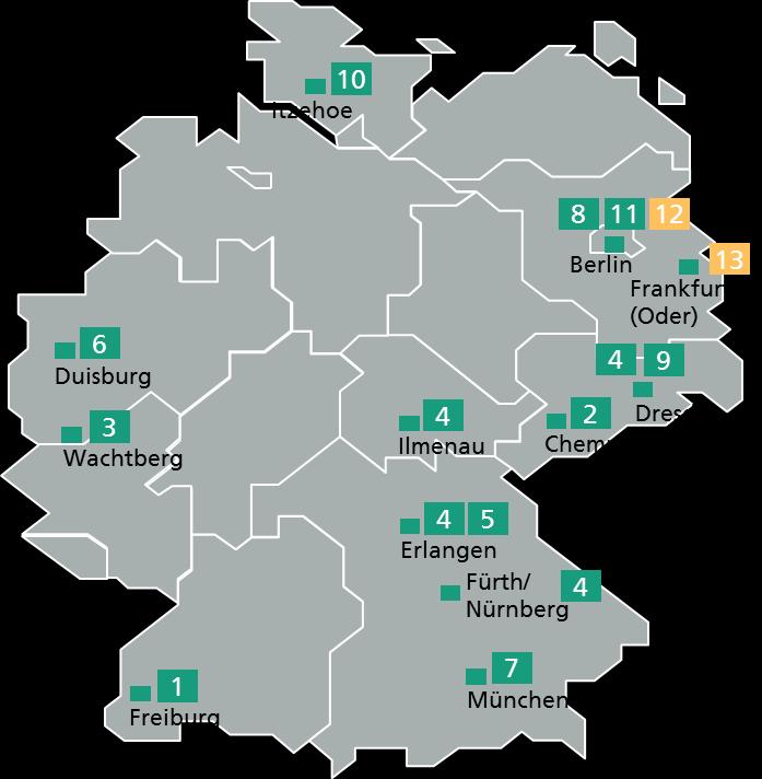
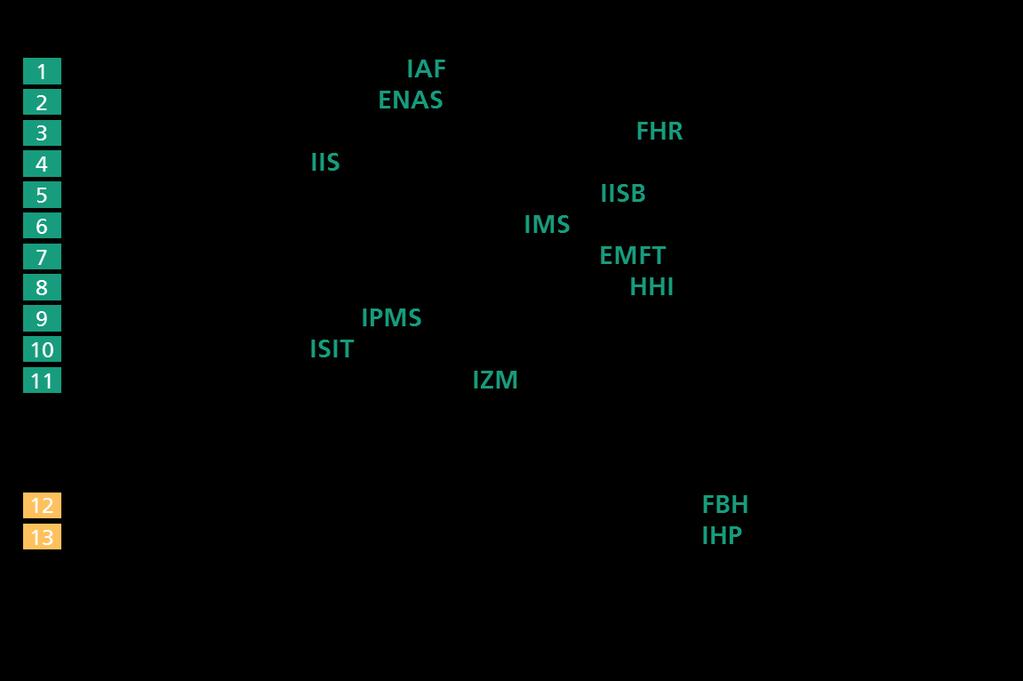
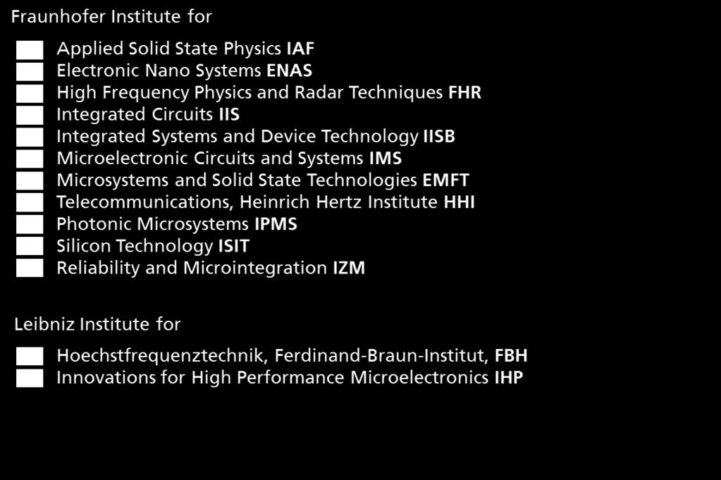
3 One-Stop-Shop for developments from wafer technologies to complete systems The FMD combines the expertise and infrastructure of 13 Research Institutes to deliver complete developments out of one hand The FMD will represent a reorganization of more than 2000 scientists and the necessary equipment for technological research and development under a single, virtual roof To prepare the FMD for future developments additional infrastructure investment of 350 Mio. is planned 3
4 Service FMD One-Stop-Shop Central contact for technology development requests Setup of research and development projects between different institutes Organisation of combined prototype and pilot fabrication Information/Organisation of technology strategies 4 4

5 Project Research Fab Microelectronics Germany Largest Federal Ministry of Education and Research Project in the area of Microelectronics Targets Setup of a virtual institute for the coordination of the cooperation partners inside the technology parks After handing over the grant approvals issued by the Federal Ministry of Education and Research, April 6, 2017 in Berlin Project volume 348,1 Mio. Eur Fraunhofer Leibniz 279,6 Mio. Eur 68,5 Mio. Eur Duration 4 years ( ) Investments in new machinery across the four technology parks: Silicon-based technologies Compound semiconductors Heterointegration Design, testing and reliability 5
6 Competencies alongside the value chain Design & Design Methods Materials and Processes Devices and Components Heterogeneous Integration / SiP Characterization, Test & Reliability Technology Plattforms 6
7 Competencies alongside the value chain Design & Design Methods Materials and Processes Devices and Components Heterogeneous Integration / SiP Characterization, Test & Reliability Design & Design Methods Microwave & Terahertz Materials and Processes Devices and Components Heterogeneous Integration / SiP Characterization, Test & Reliability Power Electronics Extended CMOS Optoelectronic Systems Sensor Systems MEMS Actuators 7


8 General competencies alongside the value chain Design & Design Methods Materials and Processes Devices and Components Heterogeneous Integration / SiP Characterization, Test & Reliability Advanced system and component design and adaption to new requirements from the application perspectives Design Methods Specification and requirement engineering Modeling and simulation, Function verification Layout Design System and component design, IP Design under constraints Prototyping Hardware-in-the-loop concepts Emulation, HW/SW co-design Foto: Fraunhofer IIS/EAS / Jürgen Lösel 8


9 General competencies alongside the value chain Design & Design Methods Materials and Processes Devices and Components Heterogeneous Integration / SiP Characterization, Test & Reliability Silicon-based and compound semiconductor based microelectronics and microsystem technology Process Technologies Material Integration CMOS, BiCMOS, FDSOI, MEMS/NEMS III-V Materials combination and processing Devices Technologies High-Frequency, Power electronics Memory Storage, Energy Harvesting Sensors, Actuators Optoelectronic devices SiC 3300V MOSFET Silicon capacities InP based optoelectronics Bulk micromachining mhemt (up to 1 THz) 9


10 General competencies alongside the value chain Design & Design Methods Materials and processes Devices and components Heterogeneous Integration / SiP Characterization, Test & Reliability Integration of all the different components from various manufacturing processes to systems Memory, CPU, FPGA Packaging MEMS, Sensors, Actors Packaging Optoelectronic/Photonic Packaging Integrated Power Device Packaging Display/RFID/Flex Packaging RF and Analog mixed signal Packaging Advanced Substrate / Interposer 10


11 General competencies alongside the value chain Design & Design Methods Materials and processes Devices and components Heterogeneous Integration / SiP Characterization, Test & Reliability Powerful methods for metrological characterization of everything, Evaluation of reliability and live time, Holistic consideration of the system function across various levels of abstraction Characterization of materials and devices General, electrical, MEMS, Opto, Power, novel Sensors Measurement and analysis of circuits and systems Analog-mixed signal / digital circuits and systems high-frequency systems characterization of hetero-integrated systems Reliability assessment Complex stress scenarios Thermal, electrical induced effects Reliability risk management Foto: Fraunhofer IZM / Jürgen Lösel 11
12 Competencies alongside the value chain Design & Design Methods Materials and Processes Devices and Components Heterogeneous Integration / SiP Characterization, Test & Reliability Microwave & Terahertz Power Electronics Extended CMOS Optoelectronic Systems Sensor Systems MEMS Actuators 12


13 Fraunhofer FHR Fraunhofer FHR Challenges in Heterointegration Integration of components from various manufacturing processes (Wafer, Chip, Passives, MEMS, Panel ) Intergration technologies for: Extreme small sizes Low power loss Large frequency range Maximum reliability Low production costs Buildup adapted to specific product design Novel solutions application-specific and customizable Cross-domain functions (optics, power electronics, signal electronics, sensor technology ) Cost-efficient production: in small batches, scalable to large volumes 3000 km 300 km Radar 14
 Scaling of 2D- and 2,5D-Integration schemes")

14 Scientific contents in Heterointegration Structure size will be adapted to the components Strategies for the realisation of extreme small structure sizes on large production formats (Chip, Wafer, Panel) Scaling of 2D- and 2,5D-Integration schemes for large area substrates and complex 3D-Stacking Extension of processes to non-electronic functionalities (cross-domain capacity, e.g. optoelectronics, optics, sensor technologies) Allocation of integration strategies and processes for smart systems 15
15 Technological Goals for the Future Integration Short term Further development up to the technological limits (geometrical structures < 750 nm, substrate size 450 x 600 mm) Integration of sensors, MEMS, compound semiconductors Buildup of multiproject platforms to reduce costs using Wafer-, Panel- and Sheet-Level Process development for the integration of power electronic, optoelectronics and RF-components into substrates; with regard to heat dissipation, precision of alignment and structure Long term Development of a smart functionality approach: integration of medium interfaces (optical, fluid, nano electronical) Development of new strategies for structuring: e.g. hybrid technologies by using combined processes (printing, laser direct imaging, stepper, imprint) 16


16 Fraunhofer FHR Technology Support Example Microwave & Terahertz Radar Applications Space to In-line-AOI Security to Spectroscopy Ultra-high Bandwidth up to 300 GHz Radar Highest achievable level of integration by integrating many components in one single SiGe- Chip Very large applicable temperature range from -40 C up to +85 C. 17


17 Fraunhofer IZM Technology Support Example Panel Level Packaging Panel Level Packaging up to 18 x 24 Embedding Components into PWB Fan-Out Packaging using Molding Applications Power Electronics Automotive Smart Cameras RF-Module Sensor Packaging LED-Packaging Medical Devices 18


18 Technology Support Example System-aware Power Packaging (Si, SiC & GaN) Application-Focus on Power Electronics: Power generation & transmission low, medium and high voltage AC/AC, AC/DC & DC/DC-converters Traction avionics, rail & automotive Vertical integrated development: Design & Simulation Material & Manufacturing SiC ( TP2) Device Packaging & Module Integration Test, analytics & forensics Reliability & Lifetime Model ( TP4) 19 Fraunhofer IISB Technology & Market Trends
 Material selection")


19 Fraunhofer IPMS Technology Support Example MEMS Actuators Full Services Offer Device and packaging construction (3D CAD) Material selection (Package, Protection, ) Simulation (thermal, optical, electrical) Methodology evaluation Chip Integration on Foil Sheets Technology Prospects Extreme planar packaging technologies for several millions micro mirrors per chip MEMS Packaging within clean room class ISO4 [US- Kl.10 fully automated assembly 20


20 Fraunhofer ISIT Technology Support Example MEMS Actuators Full Services Offer Assembly and joining of MEMS, IC and SMD components on diverse substrates Printed Interconnects System Characterization Reliabilty Testing Technology Prospects Passive adjust of optical components on wafer for WLP Sub 0.5 µm precise in-situ laser soldering W2W, C2W Bonding with nanoparticles Hermetic optical capping on wafer level Stacked and hybrid IC/MEMS Integration 21


21 Fraunhofer EMFT Technology Park 3»Heterogeneous Integration«Technology Support Example Flex Substrate Integration Current Technology State Production of high density redistribution layer on foils in Reel-to-Reel (RzR) Chip Integration on Foil Sheets Technology Improvement Integration of adaptive lithography for inline correction of the Foil Distortions within the Reel-to- Reel-process (RtR) Extremely thin and foldable Chip-Foil-Packages in RtR Module-based integration von multi- functional foil systems Foldable Sensors MEMS-IC Flexible 22


22 YOUR CONTACT Jörg Amelung Head of (FMD) Dr.-Ing. Stephan Guttowski Head of Technology Park»Heterointegration«Forschungsfabrik Mikroelektronik Deutschland FMD Anna-Louisa-Karsch-Str Berlin stephan.guttowski@mikroelektronik.fraunhofer.de GEFÖRDERT VOM 23
RESEARCH FAB MICROELECTRONICS GERMANY (FMD) The Virtual Institute for Combined Microelectronic Research and Development
 The Virtual Institute for Combined Microelectronic Research and Development") RESEARCH FAB MICROELECTRONICS GERMANY (FMD) The Virtual Institute for Combined Microelectronic Research and Development Mircoelectronic development trends Micro- and Nanoelectronics are key enabling technologies
RESEARCH FAB MICROELECTRONICS GERMANY (FMD) The Virtual Institute for Combined Microelectronic Research and Development Mircoelectronic development trends Micro- and Nanoelectronics are key enabling technologies
One-Stop-Shop for. Research Fab Microelectronics Germany
 Fraunhofer Group for Microelectronics One-Stop-Shop for Technologies and Systems Research Fab Microelectronics Germany The entire added-value chain for microelectronics and nanoelectronics from a single
FRAUNHOFER GROUP FOR MICROELECTRONICS ONE-STOP-SHOP FOR TECHNOLOGIES AND SYSTEMS
 FRAUNHOFER GROUP FOR MICROELECTRONICS ONE-STOP-SHOP FOR TECHNOLOGIES AND SYSTEMS The entire added-value chain for microelectronics and nanoelectronics from a single provider The Research Fab Microelectronics
Tailor-made R&D Services: Our Areas of Application
 One-Stop-Shop for Technologies and Systems Tailor-made R&D Services: Our Areas of Application Digital Industry: More than Developing Products The traditional industry sector is undergoing a rapid transition
Fraunhofer IZM - ASSID
 FRAUNHOFER-INSTITUT FÜR Zuverlässigkeit und Mikrointegration IZM Fraunhofer IZM - ASSID All Silicon System Integration Dresden Heterogeneous 3D Wafer Level System Integration 3D system integration is one
Packaging Roadmap: The impact of miniaturization. Bob Pfahl, inemi Celestica-iNEMI Technology Forum May 15, 2007
 Packaging Roadmap: The impact of miniaturization Bob Pfahl, inemi Celestica-iNEMI Technology Forum May 15, 2007 The Challenges for the Next Decade Addressing the consumer experience using the converged
Innovative ultra-broadband ubiquitous Wireless communications through terahertz transceivers ibrow
 Project Overview Innovative ultra-broadband ubiquitous Wireless communications through terahertz transceivers ibrow Mar-2017 Presentation outline Project key facts Motivation Project objectives Project
Smart Devices of 2025
 Smart Devices of 2025 Challenges for Packaging of Future Device Technologies Steve Riches/Kevin Cannon Tribus-D Ltd CW Workshop 27 March 2018 E:mail: info@tribus-d.uk M: 07804 980 954 Assembly Technology
IHP Innovations for High Performance Microelectronics
 IHP Innovations for High Performance Microelectronics IHP - Innovations for High Performance Microelectronics in Frankfurt (Oder) is known for internationally acknowledged research at the highest level.
Design and Modeling of Through-Silicon Vias for 3D Integration
 Design and Modeling of Through-Silicon Vias for 3D Integration Ivan Ndip, Brian Curran, Gerhard Fotheringham, Jurgen Wolf, Stephan Guttowski, Herbert Reichl Fraunhofer IZM & BeCAP @ TU Berlin IEEE Workshop
Silicon Photonics Transceivers for Hyper Scale Datacenters: Deployment and Roadmap
 Silicon Photonics Transceivers for Hyper Scale Datacenters: Deployment and Roadmap Peter De Dobbelaere Luxtera Inc. 09/19/2016 Luxtera Proprietary www.luxtera.com Luxtera Company Introduction $100B+ Shift
Project Overview. Innovative ultra-broadband ubiquitous Wireless communications through terahertz transceivers ibrow
 Project Overview Innovative ultra-broadband ubiquitous Wireless communications through terahertz transceivers ibrow Presentation outline Key facts Consortium Motivation Project objective Project description
CMP for More Than Moore
 2009 Levitronix Conference on CMP Gerfried Zwicker Fraunhofer Institute for Silicon Technology ISIT Itzehoe, Germany gerfried.zwicker@isit.fraunhofer.de Contents Moore s Law and More Than Moore Comparison:
Technology & Manufacturing
 Technology & Manufacturing Jean-Marc Chery Chief Operating Officer Front-End Manufacturing Unique capability 2 Technology portfolio aligned with application focus areas Flexible IDM model with foundry
POSSUM TM Die Design as a Low Cost 3D Packaging Alternative
 POSSUM TM Die Design as a Low Cost 3D Packaging Alternative The trend toward 3D system integration in a small form factor has accelerated even more with the introduction of smartphones and tablets. Integration
FRAUNHOFER INSTITUTE FOR PHOTONIC MICROSYSTEMS IPMS. Application Area. Quality of Life
 FRAUNHOFER INSTITUTE FOR PHOTONIC MICROSYSTEMS IPMS Application Area Quality of Life Overlay image of visible spectral range (VIS) and thermal infrared range (LWIR). Quality of Life With extensive experience
Thermal Management in the 3D-SiP World of the Future
 Thermal Management in the 3D-SiP World of the Future Presented by W. R. Bottoms March 181 th, 2013 Smaller, More Powerful Portable Devices Are Driving Up Power Density Power (both power delivery and power
450mm and Moore s Law Advanced Packaging Challenges and the Impact of 3D
 450mm and Moore s Law Advanced Packaging Challenges and the Impact of 3D Doug Anberg VP, Technical Marketing Ultratech SOKUDO Lithography Breakfast Forum July 10, 2013 Agenda Next Generation Technology
New Wave SiP solution for Power
 New Wave SiP solution for Power Vincent Lin Corporate R&D ASE Group APEC March 7 th, 2018 in San Antonio, Texas. 0 Outline Challenges Facing Human Society Energy, Environment and Traffic Autonomous Driving
EMERGING SUBSTRATE TECHNOLOGIES FOR PACKAGING
 EMERGING SUBSTRATE TECHNOLOGIES FOR PACKAGING Henry H. Utsunomiya Interconnection Technologies, Inc. Suwa City, Nagano Prefecture, Japan henryutsunomiya@mac.com ABSTRACT This presentation will outline
MEDIA RELEASE FOR IMMEDIATE RELEASE 26 JULY 2016
 MEDIA RELEASE FOR IMMEDIATE RELEASE 26 JULY 2016 A*STAR S IME KICKS OFF CONSORTIA TO DEVELOP ADVANCED PACKAGING SOLUTIONS FOR NEXT-GENERATION INTERNET OF THINGS APPLICATIONS AND HIGH-PERFORMANCE WIRELESS
Market and technology trends in advanced packaging
 Close Market and technology trends in advanced packaging Executive OVERVIEW Recent advances in device miniaturization trends have placed stringent requirements for all aspects of product manufacturing.
Flexible Hybrid Electronics Fabricated with High-Performance COTS ICs using RTI CircuitFilm TM Technology
 Flexible Hybrid Electronics Fabricated with High-Performance COTS ICs using RTI CircuitFilm TM Technology Scott Goodwin 1, Erik Vick 2 and Dorota Temple 2 1 Micross Advanced Interconnect Technology Micross
Integrated Photonics using the POET Optical InterposerTM Platform
 Integrated Photonics using the POET Optical InterposerTM Platform Dr. Suresh Venkatesan CIOE Conference Shenzhen, China Sept. 5, 2018 POET Technologies Inc. TSXV: PUBLIC POET PTK.V Technologies Inc. PUBLIC
The Future of Packaging ~ Advanced System Integration
 The Future of Packaging ~ Advanced System Integration Enabling a Microelectronic World R. Huemoeller SVP, Adv. Product / Platform Develop June 2013 Product Segments End Market % Share Summary 2 New Product
Semiconductor and LED Markets. Jon Sabol Vice President and General Manager Semiconductor and LED Division
 Semiconductor and LED Markets Jon Sabol Vice President and General Manager Semiconductor and LED Division Semiconductor & LED Investing in Semiconductor and LED $ Millions 300 200 27% CAGR 100 0 * FY06
6-7 October Marina Bay Sands Expo & Convention Centre Peony Ballroom [Level 4]
![6-7 October Marina Bay Sands Expo & Convention Centre Peony Ballroom [Level 4]](/thumbs/80/80853998.jpg "6-7 October Marina Bay Sands Expo & Convention Centre Peony Ballroom [Level 4]") camline http://www.camline.com Booth 22 camline s mission is to provide the highest quality software solutions for factory automation and logistics, helping global manufacturers maintain their competitive
camline http://www.camline.com Booth 22 camline s mission is to provide the highest quality software solutions for factory automation and logistics, helping global manufacturers maintain their competitive
R&D Requirements from the 2004 inemi Roadmap. April 7, 2005 Dr. Robert C. Pfahl, Jr. VP of Operations, inemi
 R&D Requirements from the 2004 inemi Roadmap April 7, 2005 Dr. Robert C. Pfahl, Jr. VP of Operations, inemi Topics Covered Overview of inemi and the 2004 Roadmap Situation Analysis Highlights from the
End-of-line Standard Substrates For the Characterization of organic
 FRAUNHOFER INSTITUTe FoR Photonic Microsystems IPMS End-of-line Standard Substrates For the Characterization of organic semiconductor Materials Over the last few years, organic electronics have become
MAPPER: High throughput Maskless Lithography
 MAPPER: High throughput Maskless Lithography Marco Wieland CEA- Leti Alterative Lithography workshop 1 Today s agenda Introduction Applications Qualification of on-tool metrology by in-resist metrology
Lecture: Integration of silicon photonics with electronics. Prepared by Jean-Marc FEDELI CEA-LETI
 Lecture: Integration of silicon photonics with electronics Prepared by Jean-Marc FEDELI CEA-LETI Context The goal is to give optical functionalities to electronics integrated circuit (EIC) The objectives
On-Wafer Integration of Nitrides and Si Devices: Bringing the Power of Polarization to Si
 On-Wafer Integration of Nitrides and Si Devices: Bringing the Power of Polarization to Si The MIT Faculty has made this article openly available. Please share how this access benefits you. Your story matters.
Hetero Silicon Photonics: Components, systems, packaging and beyond
 Silicon Photonics Hetero Silicon Photonics: Components, systems, packaging and beyond Thursday, October 9, 2014 Tolga Tekin and Rifat Kisacik Photonic & Plasmonic Systems, Fraunhofer for Reliability and
Nanotechnology and its effect on Electronics Manufacturing
 Nanotechnology and its effect on Electronics Manufacturing Dr. Alan Rae Vice President, Market & Business Development, NanoDynamics, Inc. Dr. Robert C. Pfahl, Jr. VP of Operations, inemi Topics Covered
Embedded Sensors. We can offer you complete solutions for intelligent integrated sensor systems.
 FRAUNHOFER-Institute For integrated Circuits IIS INTEGRATED CIRCUITS AND SYSTEMS ICS FROM AN IDEA TO A FINISHED PRODUCT WE ARE: CUSTOMER- ORIENTED PROFESSIONAL TIME-TO-MARKET- FOCUSED NETWORKED WE OFFER:
Triple i - The key to your success
 Triple i - The key to your success The needs and challenges of today s world are becoming ever more demanding. Standards are constantly rising. Creativity, reliability and high performance are basic prerequisites
RealNano & ACINTECH Projektbeispiele für Nanotechnologie in der Mikroelektronik
 RealNano & ACINTECH Projektbeispiele für Nanotechnologie in der Mikroelektronik Reinhold Ebner, Anton Köck, Stefan Defregger Materials Center Leoben Forschung GmbH Roseggerstrasse 12 A-8700 Leoben www.mcl.at
Manufacturing Development of a New Electroplated Magnetic Alloy Enabling Commercialization of PwrSoC Products
 Manufacturing Development of a New Electroplated Magnetic Alloy Enabling Commercialization of PwrSoC Products Trifon Liakopoulos, Amrit Panda, Matt Wilkowski and Ashraf Lotfi PowerSoC 2012 CONTENTS Definitions
Fiber-optic transceivers for multi-gigabit interconnects in space systems
 VTT TECHNICAL RESEARCH CENTRE OF FINLAND LTD Photo: ESA Fiber-optic transceivers for multi-gigabit interconnects in space systems at EPIC Tech Watch of Micro Photonics Expo, Berlin, 11 Oct 2016 Mikko Karppinen(mikko.karppinen@vtt.fi)
Laminate Based Fan-Out Embedded Die Technologies: The Other Option
 Laminate Based Fan-Out Embedded Die Technologies: The Other Option Theodore (Ted) G. Tessier, Tanja Karila*, Tuomas Waris*, Mark Dhaenens and David Clark FlipChip International, LLC 3701 E University Drive
Course Outcome of M.Tech (VLSI Design)
") Course Outcome of M.Tech (VLSI Design) PVL108: Device Physics and Technology The students are able to: 1. Understand the basic physics of semiconductor devices and the basics theory of PN junction. 2.
Course Outcome of M.Tech (VLSI Design) PVL108: Device Physics and Technology The students are able to: 1. Understand the basic physics of semiconductor devices and the basics theory of PN junction. 2.
TechSearch International, Inc. Corporate Overview E. Jan Vardaman, President
 TechSearch International, Inc. Corporate Overview E. Jan Vardaman, President Corporate Background Founded in 1987 and headquartered in Austin, Texas Recognized around the world as a leading consulting
MEMS Sensors: From Automotive. CE Applications. MicroNanoTec Forum Innovations for Industry April 19 th Hannover, Germany
 MEMS Sensors: From Automotive to CE Applications MicroNanoTec Forum Innovations for Industry 2010 April 19 th Hannover, Germany Oliver Schatz, CTO 1 Engineering April 2010 GmbH 2009. All rights reserved,
Hahn-Schickard Stuttgart
 Hahn-Schickard Stuttgart Hahn-Schickard Applied research for industry Budget 2016: 23,1 Mio. (5,1 Mio. industry) Employees 2016: 181 FTE (228 persons) Part of the Innovation Alliance Baden-Württemberg
3D Integration Using Wafer-Level Packaging
 3D Integration Using Wafer-Level Packaging July 21, 2008 Patty Chang-Chien MMIC Array Receivers & Spectrographs Workshop Pasadena, CA Agenda Wafer-Level Packaging Technology Overview IRAD development on
IHP Innovations for High Performance Microelectronics
 IHP Innovations for High Performance Microelectronics The IHP performs research and development in the fields of silicon-based systems, highest-frequency integrated circuits, and technologies for wireless
A Miniaturized Multi-Channel TR Module Design Based on Silicon Substrate
 Progress In Electromagnetics Research Letters, Vol. 74, 117 123, 2018 A Miniaturized Multi-Channel TR Module Design Based on Silicon Substrate Jun Zhou 1, 2, *, Jiapeng Yang 1, Donglei Zhao 1, and Dongsheng
Fraunhofer Institute for High frequency physics and radar techniques FHR. Unsere Kernkompetenzen
 Fraunhofer Institute for High frequency physics and radar techniques FHR Unsere Kernkompetenzen Unsere Kernkompetenzen KEY TECHnology radar 1 2 ABOUT Fraunhofer FHR As one of the largest radar research
Advances in CO 2 -Laser Drilling of Glass Substrates
 Available online at www.sciencedirect.com Physics Procedia 39 (2012 ) 548 555 LANE 2012 Advances in CO 2 -Laser Drilling of Glass Substrates Lars Brusberg,a, Marco Queisser b, Clemens Gentsch b, Henning
Specialization in Microelectronics. Wang Qijie Nanyang Assistant Professor in EEE March 8, 2013
 Specialization in Microelectronics Wang Qijie Nanyang Assistant Professor in EEE qjwang@ntu.edu.sg March 8, 2013 Electronic Engineering Option Microelectronics What is it about? Study of semiconductor
Hermetic Packaging Solutions using Borosilicate Glass Thin Films. Lithoglas Hermetic Packaging Solutions using Borosilicate Glass Thin Films
 Hermetic Packaging Solutions using Borosilicate Glass Thin Films 1 Company Profile Company founded in 2006 ISO 9001:2008 qualified since 2011 Headquarters and Production in Dresden, Germany Production
Power Semiconductors technologies trends for E-Mobility
 1 Power Semiconductors technologies trends for E-Mobility Gianni Vitale Power Conversion & Drives Section Manager System Lab, STMicroelectronics NESEM 2013, Toulouse All trademarks and logos are property
Des MEMS aux NEMS : évolution des technologies et des concepts aux travers des développements menés au LETI
 Des MEMS aux NEMS : évolution des technologies et des concepts aux travers des développements menés au LETI Ph. Robert 1 Content LETI at a glance From MEMS to NEMS: 30 years of technological evolution
SiP packaging technology of intelligent sensor module. Tony li
 SiP packaging technology of intelligent sensor module Tony li 2016.9 Contents What we can do with sensors Sensor market trend Challenges of sensor packaging SiP technology to overcome challenges Overview
Disruptive Developments for Advanced Die Attach to Tackle the Challenges of Heterogeneous Integration
 Disruptive Developments for Advanced Die Attach to Tackle the Challenges of Heterogeneous Integration Hugo Pristauz & Andreas Mayr, Besi Austria presented by: Stefan Behler, Besi Switzerland ECTC 2018
Opportunities and challenges of silicon photonics based System-In-Package
 Opportunities and challenges of silicon photonics based System-In-Package ECTC 2014 Panel session : Emerging Technologies and Market Trends of Silicon Photonics Speaker : Stéphane Bernabé (Leti Photonics
Challenges in Imaging, Sensors, and Signal Processing
 Challenges in Imaging, Sensors, and Signal Processing Raymond Balcerak MTO Technology Symposium March 5-7, 2007 1 Report Documentation Page Form Approved OMB No. 0704-0188 Public reporting burden for the
research in the fields of nanoelectronics
 FRAUNHOFEr center Nanoelectronic Technologies research in the fields of nanoelectronics 1 contents Fraunhofer CNT in Profile 3 Competence Areas Analytics 4 Functional Electronic Materials 5 Device & Integration
frequent Filling the gap terahertz electronics Research news from the Ferdinand-Braun-Institut
 frequent Research news from the Ferdinand-Braun-Institut Filling the gap terahertz electronics W advancement towards applications W circuits for transmitters & receivers W transferred-substrate InP heterobipolar
Trends in Advanced Packaging Technologies An IMAPS UK view
 Trends in Advanced Packaging Technologies An IMAPS UK view Andy Longford Chair IMAPS UK 2007 9 PandA Europe IMAPS UK IeMRC Interconnection event December 2008 1 International Microelectronics And Packaging
Fabricating 2.5D, 3D, 5.5D Devices
 Fabricating 2.5D, 3D, 5.5D Devices Bob Patti, CTO rpatti@tezzaron.com Tezzar on Semiconduct or 04/15/2013 1 Gen4 Dis-Integrated 3D Memory DRAM layers 42nm node 2 million vertical connections per lay per
Integrated electro-optical waveguide based devices with liquid crystals on a silicon backplane
 Integrated electro-optical waveguide based devices with liquid crystals on a silicon backplane Florenta Costache Group manager Smart Micro-Optics SMO/AMS Fraunhofer Institute for Photonic Microsystems,
Integration of Optoelectronic and RF Devices for Applications in Optical Interconnect and Wireless Communication
 Integration of Optoelectronic and RF Devices for Applications in Optical Interconnect and Wireless Communication Zhaoran (Rena) Huang Assistant Professor Department of Electrical, Computer and System Engineering
Zukunftstechnologie Dünnglasbasierte elektrooptische. Research Center of Microperipheric Technologies
 Zukunftstechnologie Dünnglasbasierte elektrooptische Baugruppenträger Dr. Henning Schröder Fraunhofer IZM, Berlin, Germany Today/Overview Motivation: external roadmaps High Bandwidth and Channel Density
Chapter 7 Introduction to 3D Integration Technology using TSV
 Chapter 7 Introduction to 3D Integration Technology using TSV Jin-Fu Li Department of Electrical Engineering National Central University Jungli, Taiwan Outline Why 3D Integration An Exemplary TSV Process
Enabling concepts: Packaging Technologies
 Enabling concepts: Packaging Technologies Ana Collado / Liam Murphy ESA / TEC-EDC 01/10/2018 ESA UNCLASSIFIED - For Official Use Enabling concepts: Packaging Technologies Drivers for the future: Higher
SAMPLE SLIDES & COURSE OUTLINE. Core Competency In Semiconductor Technology: 2. FABRICATION. Dr. Theodore (Ted) Dellin
 Dellin") & Digging Deeper Devices, Fabrication & Reliability For More Info:.com or email Dellin@ieee.org SAMPLE SLIDES & COURSE OUTLINE In : 2. A Easy, Effective, of How Devices Are.. Recommended for everyone who
& Digging Deeper Devices, Fabrication & Reliability For More Info:.com or email Dellin@ieee.org SAMPLE SLIDES & COURSE OUTLINE In : 2. A Easy, Effective, of How Devices Are.. Recommended for everyone who
Scientific Highlights 2016
 Scientific Highlights 2016 Science and Technology Sector Schools and Faculties Faculty of Science Louvain School of Engineering (EPL) Faculty of Architecture, Architectural Engineering and Urban Planning
Heterogeneous Technology Alliance. SOI MEMS Platform
 Heterogeneous Technology Alliance SOI MEMS Platform Added value of HTA SOI MEMS Platform to customers 23-Aug-11 Page 1 Attractive offering of HTA SOI MEMS Platform One-stop shop 1 Very extensive R&D resources,
Si and InP Integration in the HELIOS project
 Si and InP Integration in the HELIOS project J.M. Fedeli CEA-LETI, Grenoble ( France) ECOC 2009 1 Basic information about HELIOS HELIOS photonics ELectronics functional Integration on CMOS www.helios-project.eu
1.1 PHILOSOPHY OF MICRO/NANOFABRICATION
 CHAPTER Introduction 1 C H A P T E R C O N T E N T S 1.1 Philosophy of Micro/Nanofabrication... 1 1.2 The Industry Science Dualism... 5 1.3 Industrial Applications... 8 1.4 Purpose and Organization of
EU's contribution to research and innovation in Electronics
 EU's contribution to research and innovation in Electronics Henri.RAJBENBACH@ec.europa.eu Nikolaos.KYRLOGLOU@ec.europa.eu European Commission DG CONNECT (not legally binding presentation) SEMICON Europa-Flex
TSV MEOL (Mid-End-Of-Line) and its Assembly/Packaging Technology for 3D/2.5D Solutions
 and its Assembly/Packaging Technology for 3D/2.5D Solutions") TSV MEOL (Mid-End-Of-Line) and its Assembly/Packaging Technology for 3D/2.5D Solutions Seung Wook YOON, D.J. Na, *K. T. Kang, W. K. Choi, C.B. Yong, *Y.C. Kim and Pandi C. Marimuthu STATS ChipPAC Ltd.
TSV MEOL (Mid-End-Of-Line) and its Assembly/Packaging Technology for 3D/2.5D Solutions Seung Wook YOON, D.J. Na, *K. T. Kang, W. K. Choi, C.B. Yong, *Y.C. Kim and Pandi C. Marimuthu STATS ChipPAC Ltd.
IMAPS NE 45 A HETEROGENEOUS SIP SOLUTION FOR RF APPLICATIONS
 IMAPS NE 45 A HETEROGENEOUS SIP SOLUTION FOR RF APPLICATIONS May 1st 2018 Justin C. Borski i3 Microsystems Inc. justin.borski@i3microsystems.com A HETEROGENEOUS SIP SOLUTION FOR RF APPLICATIONS Presentation
CMOS based terahertz instrumentation for imaging and spectroscopy Matters - Kammerer, M.
 CMOS based terahertz instrumentation for imaging and spectroscopy Matters - Kammerer, M. Published in: Proceedings of the International conference on Technology and instrumentation in particle physics
Здра вствуйте, това рищи!
 Manufacturing of Smart Objects by Printing Technologies Здра вствуйте, това рищи! Moscow / RUS, June 05, 2013 Reinhard R. Baumann Chemnitz University of Technology Chair of Digital Printing Fraunhofer
Si Photonics Technology Platform for High Speed Optical Interconnect. Peter De Dobbelaere 9/17/2012
 Si Photonics Technology Platform for High Speed Optical Interconnect Peter De Dobbelaere 9/17/2012 ECOC 2012 - Luxtera Proprietary www.luxtera.com Overview Luxtera: Introduction Silicon Photonics: Introduction
ITRS Update (and the European situation) Mart Graef Delft University of Technology
 Mart Graef Delft University of Technology") ITRS Update (and the European situation) Mart Graef Delft University of Technology Overview Roadmapping: Moore s Law & More than Moore Europe and the Roadmap Beyond CMOS: Nano-Tec Infrastructures: ENI2
ITRS Update (and the European situation) Mart Graef Delft University of Technology Overview Roadmapping: Moore s Law & More than Moore Europe and the Roadmap Beyond CMOS: Nano-Tec Infrastructures: ENI2
Continuous Wave SSPAs. Version 1.6
 Continuous Wave SSPAs Version 1.6 Date: Jun 1, 2015 CONTENT Product Overview... 3 FACTS ON THE TECHNOLOGY... 4 SOLID-STATE POWER AMPLIFIERS... 5 ABOUT NANOWAVE... 8 RF Components and Subsystems NANOWAVE
3D TSV Micro Cu Column Chip-to-Substrate/Chip Assmbly/Packaging Technology
 3D TSV Micro Cu Column Chip-to-Substrate/Chip Assmbly/Packaging Technology by Seung Wook Yoon, *K. T. Kang, W. K. Choi, * H. T. Lee, Andy C. B. Yong and Pandi C. Marimuthu STATS ChipPAC LTD, 5 Yishun Street
The 3D silicon leader. March 2012
 The 3D silicon leader March 2012 IPDiA overview Company located in Caen, Normandy, France Dedicated to manufacturing of integrated passive devices Employing 100 people and operating own wafer fab Strong
Application-Based Opportunities for Reused Fab Lines
 Application-Based Opportunities for Reused Fab Lines Semicon China, March 17 th 2010 Keith Best Simax Lithography S I M A X A L L I A N C E P A R T N E R S Outline Market: Exciting More than Moore applications
Progress Towards Computer-Aided Design For Complex Photonic Integrated Circuits
 Department of Electrical and Computer Engineering Progress Towards Computer-Aided Design For Complex Photonic Integrated Circuits Wei-Ping Huang Department of Electrical and Computer Engineering McMaster
MEMS in ECE at CMU. Gary K. Fedder
 MEMS in ECE at CMU Gary K. Fedder Department of Electrical and Computer Engineering and The Robotics Institute Carnegie Mellon University Pittsburgh, PA 15213-3890 fedder@ece.cmu.edu http://www.ece.cmu.edu/~mems
Gallium Nitride & Related Wide Bandgap Materials and Devices
 Gallium Nitride & Related Wide Bandgap Materials and Devices Dr. Edgar J. Martinez Program Manager DARPATech 2000 GaAs IC Markets 1999 Market $11 Billion 2005 Market $20 Billion Consumers 2% Computers
EURIPIDES Office 17, rue de l Amiral HAMELIN Paris cedex 16 FRANCE SAB - STRATEGY RESEARCH AGENDA EURIPIDES. September 2010 version 1
 EURIPIDES Office 17, rue de l Amiral HAMELIN 75783 Paris cedex 16 FRANCE EURIPIDES SAB - STRATEGY RESEARCH AGENDA September 2010 version 1 INTRODUCTION AND EURIPIDES POSITION INSIDE EUREKA EUREKA and its
Advanced Stepper Lithography Technology to Enable Flexible AMOLED Displays. Keith Best Roger McCleary Elvino M da Silveira 5/19/17
 Advanced Stepper Lithography Technology to Enable Flexible AMOLED Displays Keith Best Roger McCleary Elvino M da Silveira 5/19/17 Agenda About Rudolph JetStep G System overview and performance Display
Plan Optik AG. Plan Optik AG PRODUCT CATALOGUE
 Plan Optik AG Plan Optik AG PRODUCT CATALOGUE 2 In order to service the high demand of wafers more quickly, Plan Optik provides off the shelf products in sizes from 2 up to 300mm diameter. Therefore Plan
Beyond Moore the challenge for Europe
 Beyond Moore the challenge for Europe Dr. Alfred J. van Roosmalen Vice-President Business Development, NXP Semiconductors Company member of MEDEA+/CATRENE/AENEAS/Point-One FIT-IT 08 Spring Research Wien,
T/R Modules. Version 1.0
 T/R Modules Version 1.0 Date: Jun 1, 2015 CONTENT Product Overview... 3 FACTS ON THE TECHNOLOGY... 4 ABOUT NANOWAVE... 6 RF Components and Subsystems NANOWAVE Technologies Inc. is a privately owned Canadian
First Demonstration of Panel Glass Fan-out (GFO) Packages for High I/O Density and High Frequency Multi-Chip Integration
 Packages for High I/O Density and High Frequency Multi-Chip Integration") First Demonstration of Panel Glass Fan-out (GFO) Packages for High I/O Density and High Frequency Multi-Chip Integration Tailong Shi, Chintan Buch,Vanessa Smet, Yoichiro Sato, Lutz Parthier, Frank Wei
First Demonstration of Panel Glass Fan-out (GFO) Packages for High I/O Density and High Frequency Multi-Chip Integration Tailong Shi, Chintan Buch,Vanessa Smet, Yoichiro Sato, Lutz Parthier, Frank Wei
MMIC: Introduction. Evangéline BENEVENT. Università Mediterranea di Reggio Calabria DIMET
 Evangéline BENEVENT Università Mediterranea di Reggio Calabria DIMET 1 Evolution of electronic circuits: high frequency and complexity Moore s law More than Moore System-In-Package System-On-Package Applications
5G Systems and Packaging Opportunities
 5G Systems and Packaging Opportunities Rick Sturdivant, Ph.D. Founder and Chief Technology Officer MPT, Inc. (www.mptcorp.com), ricksturdivant@gmail.com Abstract 5G systems are being developed to meet
AIR-COUPLED PHOTOCONDUCTIVE ANTENNAS
 AIR-COUPLED PHOTOCONDUCTIVE ANTENNAS Report: Air-Coupled Photoconductive Antennas In this paper, we present air-coupled terahertz photoconductive antenna (THz-PCAs) transmitters and receivers made on high-resistive
Glenn G. Daves. Director, Packaging Solutions Development Freescale Semiconductor, Inc.
 Glenn G. Daves Director, Packaging Solutions Development Freescale Semiconductor, Inc. Freescale, the Freescale logo, AltiVec, C-5, CodeTEST, CodeWarrior, ColdFire, C-Ware, t he Energy Efficient Solutions
Yole Developpement. Developpement-v2585/ Publisher Sample
 Yole Developpement http://www.marketresearch.com/yole- Developpement-v2585/ Publisher Sample Phone: 800.298.5699 (US) or +1.240.747.3093 or +1.240.747.3093 (Int'l) Hours: Monday - Thursday: 5:30am - 6:30pm
Design, Characterization & Modelling of a CMOS Magnetic Field Sensor
 Design, Characteriation & Modelling of a CMOS Magnetic Field Sensor L. Latorre,, Y.Bertrand, P.Haard, F.Pressecq, P.Nouet LIRMM, UMR CNRS / Universit de Montpellier II, Montpellier France CNES, Quality
3D ICs: Recent Advances in the Industry
 3D ICs: Recent Advances in the Industry Suresh Ramalingam Senior Director, Advanced Packaging Outline 3D IC Background 3D IC Technology Development Summary Acknowledgements Stacked Silicon Interconnect
Reducing MEMS product development and commercialization time
 Reducing MEMS product development and commercialization time Introduction Fariborz Maseeh, Andrew Swiecki, Nora Finch IntelliSense Corporation 36 Jonspin Road, Wilmington MA 01887 www.intellisense.com
Feature-level Compensation & Control
 Feature-level Compensation & Control 2 Sensors and Control Nathan Cheung, Kameshwar Poolla, Costas Spanos Workshop 11/19/2003 3 Metrology, Control, and Integration Nathan Cheung, UCB SOI Wafers Multi wavelength