How material engineering contributes to delivering innovation in the hyper connected world
|
|
|
- Barnaby Reeves
- 5 years ago
- Views:
Transcription

1 How material engineering contributes to delivering innovation in the hyper connected world Paul BOUDRE, Soitec CEO Leti Innovation Days - July 2018 Grenoble, France


2 We live in a world of data In perpetual contact with data Our connected life Connect with each other and the world around us


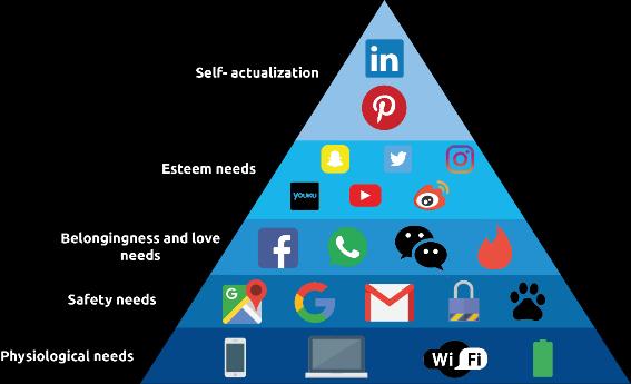
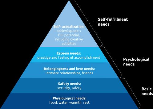
3 A new hierarchy of needs Maslow s Pyramid of Needs Maslow s Pyramid 2.0


4 Turning data into meaningful information Efficiency Knowledge Security Health Improving the way we live, work, learn and play


5 Electronics is the backbone of society Performance Cost Power Form factor Reliability The semiconductor industry pushes boundaries To meet new needs


6 Substrates are the foundation of high-tech products Services Final Product Software Hardware Semiconductor device Substrates The characteristics of the initial substrate define the performance and architecture of devices and circuits
7 Material innovation


8 An intricate relationship between substrate and device Superior effective resistivity Engineered substrates vs bulk Reduced crosstalk & energy loss Improved linearity RF-eSI HR-SOI Source : Substrate related RF performance on Trap-Rich High Resistivity SOI wafers, Khaled Ben Ali, Thesis, 2014 Bulk


 Crystal")
 Si")
9 Substrate engineering through Smart Cut TM Technology Crystalline layer engineering Combination with insulating layer Crystal on Crystal (lattice compatible) Amorphous on Amorphous Crystal on Crystal (not lattice compatible) Crystal on Amorphous Example: SOI (Silicon-on-Insulator) Si on SiO2 Smart-Cut TM Thin & highly uniform layers

10 Atomic scale layer transfer uniformity Native oxide Crystalline silicon 14 atomic planes ~ 3.8nm Buried oxide


11 Which benefits does material innovation bring? End Product Benefits Device quality and functionality improvement Substrate Pre-processing of active layers with unique properties


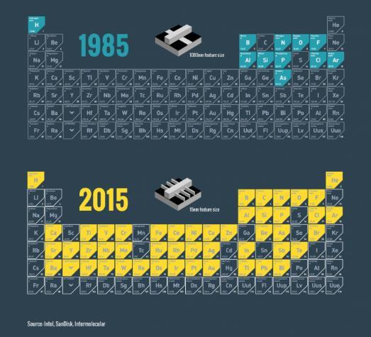
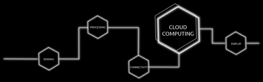
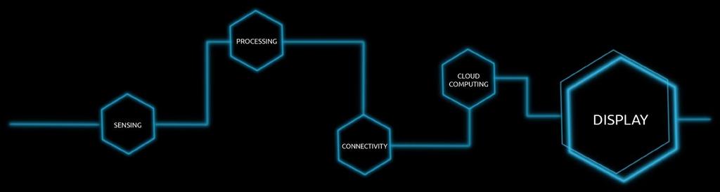
12 100 mm 150 mm Substrate wafer sizes 200 mm 300 mm This is what we do at Soitec This is not Soitec's full portfolio, but a broad outline of it SENSING IMAGER PROCESSING DIGITAL TO MIXED-SIGNAL CONNECTIVITY RF COMPUTING PHOTONICS DISPLAY EMERGING TECHNOLOGIES 100% of smartphones contain RF-SOI
13 Collaboration all along the value chain is required to improve PPAC* + reliability and speed up end products innovations Services Final Product Software Hardware Semiconductor device Substrates *PPAC = Power, Performance, Area (Form Factor), Cost


14 25 years of joint development with the Leti Increased development speed to enable breakthrough solutions -Smart Cut


15 Substrates: a unique & powerful innovation platform. SMART EVERYTHING Services Final Product Software ICs & Systems Innovation Platforms Hardware Semiconductor device Substrates Substrate Innovation Center

16 Shortening the R&D to solution cycle Fabless System innovation platforms & ecosystem & Academia Substrate Innovation Center Substrate Solutions Sampling & Prototyping Exploratory Solutions New Applications Equipment Materials

17 What does material innovation bring? Technological breakthroughs, unlocking hidden value Material innovation and substrate engineering made entirely new horizons possible
18


19 Sensing everything - even the invisible More data means that an increasingly larger portion of the electromagnetic spectrum has to be used to: Capture data Communicate data


 New")


20 3D image sensing: Imager-SOI for NIR Silicium not working well in Near Infrared (NIR) New material required (with reflective layer) to boost quantum efficiency Imager-SOI solution
21


22 AI and machine learning are increasingly being pushed from the cloud to the edge 4 drivers pushing AI at the edge Classifying raw data into metadata Examples of applications Latency Data privacy Giga/Mega bytes per second of incoming raw data from sensors Home Assistant Power consumption Automotive Cost Few (kilo) bytes per second of outgoing, heavily processed minimum joule per operation


23 Variation of chip characteristics Variation of chip characteristics FD-SOI engineered substrates enable embedded AI at the edge Superior transistor behavior Ultimate power efficiency thanks to dynamic Vth control (body bias) Bulk FD-SOI Without Body Bias With Body Bias Maximum design margins Reduced design margins Better electrostatics Lower variability Dynamic Vth control Simpler manufacturing Vdd min ~0.4V Minimum Energy Point *Vth = Threshold voltage
24
 RF-SOI 7 BULK (3D FinFET) FD-SOI FD-SOI with RF")
25 Technology node SOI enables RF-CMOS technologies Enhanced signal integrity BULK (Planar) RF-SOI 7 BULK (3D FinFET) FD-SOI FD-SOI with RF option


26 Number of bands and bands combinations New filter technologies are needed for 5G CHALLENGES More bands and band combinations Larger bands and higher frequency bands Band density in the spectrum Cost and manufacturability NEW ENGINEERED SUBSTRATE Filter template Bulk acoustic filter POI acoustic filter
27


28 Massive growth in data transmission Photonics-SOI wafer Optical waveguide for silicon integrated photonic systems High speed, long range, low power optical transceivers for next generation datacenters
29


30 Disruptive engineered substrates for microled displays Engineered substrate Red/Green/Blue MicroLEDs High brightness, high resolution, low power consumption microleds for next generation displays
31 Data Revolution An increasingly higher degree of sensing, processing and communications capability is being embedded into physical objects to bring intelligence to their operation

32 Material innovation fosters data Revolution Future systems require new materials for exciting innovations Material innovation powers society's continued digital transformation
33 Soitec
SOI technology platforms for 5G: Opportunities of collaboration
 SOI technology platforms for 5G: Opportunities of collaboration Dr. Ionut RADU Director, R&D SOITEC MOS AK workshop, Silicon Valley December 6th, 2017 Sourcing value from substrate Robert E. White ISBN-13:
Engineered substrates - at the heart of 4G/5G FEM evolution
 Engineered substrates - at the heart of 4G/5G FEM evolution Bernard ASPAR EVP Communication & Power Business Unit, Soitec SOI Consortium, Shanghai, September 2018 1 FEM market 2 RF-SOI 3 POI RF FEM market
FinFET vs. FD-SOI Key Advantages & Disadvantages
 FinFET vs. FD-SOI Key Advantages & Disadvantages Amiad Conley Technical Marketing Manager Process Diagnostics & Control, Applied Materials ChipEx-2014, Apr 2014 1 Moore s Law The number of transistors
Alternatives to standard MOSFETs. What problems are we really trying to solve?
 Alternatives to standard MOSFETs A number of alternative FET schemes have been proposed, with an eye toward scaling up to the 10 nm node. Modifications to the standard MOSFET include: Silicon-in-insulator
HOW TO CONTINUE COST SCALING. Hans Lebon
 HOW TO CONTINUE COST SCALING Hans Lebon OUTLINE Scaling & Scaling Challenges Imec Technology Roadmap Wafer size scaling : 450 mm 2 COST SCALING IMPROVED PERFORMANCE 3 GLOBAL TRAFFIC FORECAST Cloud Traffic
LSI ON GLASS SUBSTRATES
 LSI ON GLASS SUBSTRATES OUTLINE Introduction: Why System on Glass? MOSFET Technology Low-Temperature Poly-Si TFT Technology System-on-Glass Technology Issues Conclusion System on Glass CPU SRAM DRAM EEPROM
Session 3: Solid State Devices. Silicon on Insulator
 Session 3: Solid State Devices Silicon on Insulator 1 Outline A B C D E F G H I J 2 Outline Ref: Taurand Ning 3 SOI Technology SOl materials: SIMOX, BESOl, and Smart Cut SIMOX : Synthesis by IMplanted
Semiconductor Process Reliability SVTW 2012 Esko Mikkola, Ph.D. & Andrew Levy
 Semiconductor Process Reliability SVTW 2012 Esko Mikkola, Ph.D. & Andrew Levy 1 IC Failure Modes Affecting Reliability Via/metallization failure mechanisms Electro migration Stress migration Transistor
EUROSOI+- FP of 38 30/06/ FINAL PUBLISHABLE SUMMARY REPORT
 EUROSOI+- FP7-216373 3 of 38 30/06/2011 1. FINAL PUBLISHABLE SUMMARY REPORT EUROSOI+- FP7-216373 4 of 38 30/06/2011 EUROSOI+- FP7-216373 5 of 38 30/06/2011 The main and last objective of EUROSOI Network
Silicon Photonics Technology Platform To Advance The Development Of Optical Interconnects
 Silicon Photonics Technology Platform To Advance The Development Of Optical Interconnects By Mieke Van Bavel, science editor, imec, Belgium; Joris Van Campenhout, imec, Belgium; Wim Bogaerts, imec s associated
PERSPECTIVES FOR DISRUPTIVE 200MM/8-INCH GAN POWER DEVICE AND GAN-IC TECHNOLOGY DR. DENIS MARCON SR. BUSINESS DEVELOPMENT MANAGER
 PERSPECTIVES FOR DISRUPTIVE 200MM/8-INCH GAN POWER DEVICE AND GAN-IC TECHNOLOGY DR. DENIS MARCON SR. BUSINESS DEVELOPMENT MANAGER What I will show you today 200mm/8-inch GaN-on-Si e-mode/normally-off technology
Silicon photonics integration roadmap for applications in computing systems
 Silicon photonics integration roadmap for applications in computing systems Bert Jan Offrein Neuromorphic Devices and Systems Group 2016 IBM Corporation Outline Photonics and computing? The interconnect
ITRS MOSFET Scaling Trends, Challenges, and Key Technology Innovations
 Workshop on Frontiers of Extreme Computing Santa Cruz, CA October 24, 2005 ITRS MOSFET Scaling Trends, Challenges, and Key Technology Innovations Peter M. Zeitzoff Outline Introduction MOSFET scaling and
NEXT GENERATION SILICON PHOTONICS FOR COMPUTING AND COMMUNICATION PHILIPPE ABSIL
 NEXT GENERATION SILICON PHOTONICS FOR COMPUTING AND COMMUNICATION PHILIPPE ABSIL OUTLINE Introduction Platform Overview Device Library Overview What s Next? Conclusion OUTLINE Introduction Platform Overview
Fin-Shaped Field Effect Transistor (FinFET) Min Ku Kim 03/07/2018
 Min Ku Kim 03/07/2018") Fin-Shaped Field Effect Transistor (FinFET) Min Ku Kim 03/07/2018 ECE 658 Sp 2018 Semiconductor Materials and Device Characterizations OUTLINE Background FinFET Future Roadmap Keeping up w/ Moore s Law
Fin-Shaped Field Effect Transistor (FinFET) Min Ku Kim 03/07/2018 ECE 658 Sp 2018 Semiconductor Materials and Device Characterizations OUTLINE Background FinFET Future Roadmap Keeping up w/ Moore s Law
FD-SOI FOR RF IC DESIGN. SITRI LETI Workshop Mercier Eric 08 september 2016
 FD-SOI FOR RF IC DESIGN SITRI LETI Workshop Mercier Eric 08 september 2016 UTBB 28 nm FD-SOI : RF DIRECT BENEFITS (1/2) 3 back-end options available Routing possible on the AluCap level no restriction
Towards a Reconfigurable Nanocomputer Platform
 Towards a Reconfigurable Nanocomputer Platform Paul Beckett School of Electrical and Computer Engineering RMIT University Melbourne, Australia 1 The Nanoscale Cambrian Explosion Disparity: Widerangeof
Lecture: Integration of silicon photonics with electronics. Prepared by Jean-Marc FEDELI CEA-LETI
 Lecture: Integration of silicon photonics with electronics Prepared by Jean-Marc FEDELI CEA-LETI Context The goal is to give optical functionalities to electronics integrated circuit (EIC) The objectives
 www.soiconsortium.org By Xavier CAUCHY, Digital Applications Manager, Soitec xavier.cauchy@soitec.fr with François ANDRIEU, Senior Research Engineer, LETI April 2010 SOI Industry Consortium Questions and
ICT Micro- and nanoelectronics technologies
 EPoSS Proposers' Day, 2 Feb 2017, Brussels ICT 31-2017 Micro- and nanoelectronics technologies Eric Fribourg-Blanc, Henri Rajbenbach, Andreas Lymberis European Commission DG CONNECT (Communications Networks,
ULS24 Frequently Asked Questions
 List of Questions 1 1. What type of lens and filters are recommended for ULS24, where can we source these components?... 3 2. Are filters needed for fluorescence and chemiluminescence imaging, what types
Advanced PDK and Technologies accessible through ASCENT
 Advanced PDK and Technologies accessible through ASCENT MOS-AK Dresden, Sept. 3, 2018 L. Perniola*, O. Rozeau*, O. Faynot*, T. Poiroux*, P. Roseingrave^ olivier.faynot@cea.fr *Cea-Leti, Grenoble France;
Research Needs for Device Sciences Modeling and Simulation (May 6, 2005)
") Research Needs for Device Sciences Modeling and Simulation (May 6, 2005) SRC Device Sciences 2005 Modeling and Simulation Task Force Contributing organizations: Axcelis, Freescale, IBM, Intel, LSI, SRC,
Research Needs for Device Sciences Modeling and Simulation (May 6, 2005) SRC Device Sciences 2005 Modeling and Simulation Task Force Contributing organizations: Axcelis, Freescale, IBM, Intel, LSI, SRC,
IEEE JOURNAL OF SELECTED TOPICS IN QUANTUM ELECTRONICS 2010 Silicon Photonic Circuits: On-CMOS Integration, Fiber Optical Coupling, and Packaging
 IEEE JOURNAL OF SELECTED TOPICS IN QUANTUM ELECTRONICS 2010 Silicon Photonic Circuits: On-CMOS Integration, Fiber Optical Coupling, and Packaging Christophe Kopp, St ephane Bernab e, Badhise Ben Bakir,
Integrated Photonics using the POET Optical InterposerTM Platform
 Integrated Photonics using the POET Optical InterposerTM Platform Dr. Suresh Venkatesan CIOE Conference Shenzhen, China Sept. 5, 2018 POET Technologies Inc. TSXV: PUBLIC POET PTK.V Technologies Inc. PUBLIC
Nanotechnology, the infrastructure, and IBM s research projects
 Nanotechnology, the infrastructure, and IBM s research projects Dr. Paul Seidler Coordinator Nanotechnology Center, IBM Research - Zurich Nanotechnology is the understanding and control of matter at dimensions
MAPPER: High throughput Maskless Lithography
 MAPPER: High throughput Maskless Lithography Marco Wieland CEA- Leti Alterative Lithography workshop 1 Today s agenda Introduction Applications Qualification of on-tool metrology by in-resist metrology
Monolithic Pixel Sensors in SOI technology R&D activities at LBNL
 Monolithic Pixel Sensors in SOI technology R&D activities at LBNL Lawrence Berkeley National Laboratory M. Battaglia, L. Glesener (UC Berkeley & LBNL), D. Bisello, P. Giubilato (LBNL & INFN Padova), P.
More specifically, I would like to talk about Gallium Nitride and related wide bandgap compound semiconductors.
 Good morning everyone, I am Edgar Martinez, Program Manager for the Microsystems Technology Office. Today, it is my pleasure to dedicate the next few minutes talking to you about transformations in future
sensors & systems Imagine future imaging... Leti, technology research institute Contact:
 Imaging sensors & systems Imagine future imaging... Leti, technology research institute Contact: leti.contact@cea.fr From consumer markets to high-end applications smart home IR array for human activity
Image sensor combining the best of different worlds
 Image sensors and vision systems Image sensor combining the best of different worlds First multispectral time-delay-and-integration (TDI) image sensor based on CCD-in-CMOS technology. Introduction Jonathan
New advances in silicon photonics Delphine Marris-Morini
 New advances in silicon photonics Delphine Marris-Morini P. Brindel Alcatel-Lucent Bell Lab, Nozay, France New Advances in silicon photonics D. Marris-Morini, L. Virot*, D. Perez-Galacho, X. Le Roux, D.
Lecture 4 - Digital Representations III + Transistors
 Lecture 4 - Digital Representations III + Transistors Video: Seems like a natural extension from images no? We just have a new dimension (time) Each frame is just an image made up of pixels Display n frames
420 Intro to VLSI Design
 Dept of Electrical and Computer Engineering 420 Intro to VLSI Design Lecture 0: Course Introduction and Overview Valencia M. Joyner Spring 2005 Getting Started Syllabus About the Instructor Labs, Problem
Beyond Moore the challenge for Europe
 Beyond Moore the challenge for Europe Dr. Alfred J. van Roosmalen Vice-President Business Development, NXP Semiconductors Company member of MEDEA+/CATRENE/AENEAS/Point-One FIT-IT 08 Spring Research Wien,
Silicon on Insulator (SOI) Spring 2018 EE 532 Tao Chen
 Spring 2018 EE 532 Tao Chen") Silicon on Insulator (SOI) Spring 2018 EE 532 Tao Chen What is Silicon on Insulator (SOI)? SOI silicon on insulator, refers to placing a thin layer of silicon on top of an insulator such as SiO2. The devices
Silicon on Insulator (SOI) Spring 2018 EE 532 Tao Chen What is Silicon on Insulator (SOI)? SOI silicon on insulator, refers to placing a thin layer of silicon on top of an insulator such as SiO2. The devices
Intel s High-k/Metal Gate Announcement. November 4th, 2003
 Intel s High-k/Metal Gate Announcement November 4th, 2003 1 What are we announcing? Intel has made significant progress in future transistor materials Two key parts of this new transistor are: The gate
Simulation of High Resistivity (CMOS) Pixels
 Pixels") Simulation of High Resistivity (CMOS) Pixels Stefan Lauxtermann, Kadri Vural Sensor Creations Inc. AIDA-2020 CMOS Simulation Workshop May 13 th 2016 OUTLINE 1. Definition of High Resistivity Pixel Also
Simulation of High Resistivity (CMOS) Pixels Stefan Lauxtermann, Kadri Vural Sensor Creations Inc. AIDA-2020 CMOS Simulation Workshop May 13 th 2016 OUTLINE 1. Definition of High Resistivity Pixel Also
Resonant Tunneling Device. Kalpesh Raval
 Resonant Tunneling Device Kalpesh Raval Outline Diode basics History of Tunnel diode RTD Characteristics & Operation Tunneling Requirements Various Heterostructures Fabrication Technique Challenges Application
Lecture #29. Moore s Law
 Lecture #29 ANNOUNCEMENTS HW#15 will be for extra credit Quiz #6 (Thursday 5/8) will include MOSFET C-V No late Projects will be accepted after Thursday 5/8 The last Coffee Hour will be held this Thursday
Enabling Breakthroughs In Technology
 Enabling Breakthroughs In Technology Mike Mayberry Director of Components Research VP, Technology and Manufacturing Group Intel Corporation June 2011 Defined To be defined Enabling a Steady Technology
IOLTS th IEEE International On-Line Testing Symposium
 IOLTS 2018 24th IEEE International On-Line Testing Symposium Exp. comparison and analysis of the sensitivity to laser fault injection of CMOS FD-SOI and CMOS bulk technologies J.M. Dutertre 1, V. Beroulle
Monolithic Pixel Detector in a 0.15µm SOI Technology
 Monolithic Pixel Detector in a 0.15µm SOI Technology 2006 IEEE Nuclear Science Symposium, San Diego, California, Nov. 1, 2006 Yasuo Arai (KEK) KEK Detector Technology Project : [SOIPIX Group] Y. Arai Y.
GSEF 2019 Advisory Board
 GSEF 2019 Advisory Board Ralph Lauxmann, Senior Vice President Systems & Technology, Continental Automotive Hans Adlkofer, Vice President Systems Group, The Automotive Division, Infineon Technologies Hai
Opportunities and challenges of silicon photonics based System-In-Package
 Opportunities and challenges of silicon photonics based System-In-Package ECTC 2014 Panel session : Emerging Technologies and Market Trends of Silicon Photonics Speaker : Stéphane Bernabé (Leti Photonics
Sub-micron technology IC fabrication process trends SOI technology. Development of CMOS technology. Technology problems due to scaling
 Goodbye Microelectronics Welcome Nanoelectronics Sub-micron technology IC fabrication process trends SOI technology SiGe Tranzistor in 50nm process Virus The thickness of gate oxide= 1.2 nm!!! Today we
CHAPTER 2 POLARIZATION SPLITTER- ROTATOR BASED ON A DOUBLE- ETCHED DIRECTIONAL COUPLER
 CHAPTER 2 POLARIZATION SPLITTER- ROTATOR BASED ON A DOUBLE- ETCHED DIRECTIONAL COUPLER As we discussed in chapter 1, silicon photonics has received much attention in the last decade. The main reason is
Innovative ultra-broadband ubiquitous Wireless communications through terahertz transceivers ibrow
 Project Overview Innovative ultra-broadband ubiquitous Wireless communications through terahertz transceivers ibrow Mar-2017 Presentation outline Project key facts Motivation Project objectives Project
EMT 251 Introduction to IC Design
 EMT 251 Introduction to IC Design (Pengantar Rekabentuk Litar Terkamir) Semester II 2011/2012 Introduction to IC design and Transistor Fundamental Some Keywords! Very-large-scale-integration (VLSI) is
Electronic-Photonic ICs for Low Cost and Scalable Datacenter Solutions
 Electronic-Photonic ICs for Low Cost and Scalable Datacenter Solutions Christoph Theiss, Director Packaging Christoph.Theiss@sicoya.com 1 SEMICON Europe 2016, October 27 2016 Sicoya Overview Spin-off from
Silicon Photonics Photo-Detector Announcement. Mario Paniccia Intel Fellow Director, Photonics Technology Lab
 Silicon Photonics Photo-Detector Announcement Mario Paniccia Intel Fellow Director, Photonics Technology Lab Agenda Intel s Silicon Photonics Research 40G Modulator Recap 40G Photodetector Announcement
Intel s Breakthrough in High-K Gate Dielectric Drives Moore s Law Well into the Future
 Page 1 Intel s Breakthrough in High-K Gate Dielectric Drives Moore s Law Well into the Future Robert S. Chau Intel Fellow, Technology and Manufacturing Group Director, Transistor Research Intel Corporation
Lithography in our Connected World
 Lithography in our Connected World SEMI Austin Spring Forum TOP PAN P R INTING CO., LTD MATER IAL SOLUTIONS DIVISION Toppan Printing Co., LTD A Broad-Based Global Printing Company Foundation: January 17,
Challenges in Imaging, Sensors, and Signal Processing
 Challenges in Imaging, Sensors, and Signal Processing Raymond Balcerak MTO Technology Symposium March 5-7, 2007 1 Report Documentation Page Form Approved OMB No. 0704-0188 Public reporting burden for the
Photonic Crystal Slot Waveguide Spectrometer for Detection of Methane
 Photonic Crystal Slot Waveguide Spectrometer for Detection of Methane Swapnajit Chakravarty 1, Wei-Cheng Lai 2, Xiaolong (Alan) Wang 1, Che-Yun Lin 2, Ray T. Chen 1,2 1 Omega Optics, 10306 Sausalito Drive,
Optical Bus for Intra and Inter-chip Optical Interconnects
 Optical Bus for Intra and Inter-chip Optical Interconnects Xiaolong Wang Omega Optics Inc., Austin, TX Ray T. Chen University of Texas at Austin, Austin, TX Outline Perspective of Optical Backplane Bus
High speed silicon-based optoelectronic devices Delphine Marris-Morini Institut d Electronique Fondamentale, Université Paris Sud
 High speed silicon-based optoelectronic devices Delphine Marris-Morini Institut d Electronique Fondamentale, Université Paris Sud Data centers Optical telecommunications Environment Interconnects Silicon
Transistor was first invented by William.B.Shockley, Walter Brattain and John Bardeen of Bell Labratories. In 1961, first IC was introduced.
 Unit 1 Basic MOS Technology Transistor was first invented by William.B.Shockley, Walter Brattain and John Bardeen of Bell Labratories. In 1961, first IC was introduced. Levels of Integration:- i) SSI:-
MEDIA RELEASE FOR IMMEDIATE RELEASE 26 JULY 2016
 MEDIA RELEASE FOR IMMEDIATE RELEASE 26 JULY 2016 A*STAR S IME KICKS OFF CONSORTIA TO DEVELOP ADVANCED PACKAGING SOLUTIONS FOR NEXT-GENERATION INTERNET OF THINGS APPLICATIONS AND HIGH-PERFORMANCE WIRELESS
Basic Fabrication Steps
 Basic Fabrication Steps and Layout Somayyeh Koohi Department of Computer Engineering Adapted with modifications from lecture notes prepared by author Outline Fabrication steps Transistor structures Transistor
Fundamentals of CMOS Image Sensors
 CHAPTER 2 Fundamentals of CMOS Image Sensors Mixed-Signal IC Design for Image Sensor 2-1 Outline Photoelectric Effect Photodetectors CMOS Image Sensor(CIS) Array Architecture CIS Peripherals Design Considerations
MEMS in ECE at CMU. Gary K. Fedder
 MEMS in ECE at CMU Gary K. Fedder Department of Electrical and Computer Engineering and The Robotics Institute Carnegie Mellon University Pittsburgh, PA 15213-3890 fedder@ece.cmu.edu http://www.ece.cmu.edu/~mems
3-D Modelling of the Novel Nanoscale Screen-Grid Field Effect Transistor (SGFET)
") 3-D Modelling of the Novel Nanoscale Screen-Grid Field Effect Transistor (SGFET) Pei W. Ding, Kristel Fobelets Department of Electrical Engineering, Imperial College London, U.K. J. E. Velazquez-Perez
3-D Modelling of the Novel Nanoscale Screen-Grid Field Effect Transistor (SGFET) Pei W. Ding, Kristel Fobelets Department of Electrical Engineering, Imperial College London, U.K. J. E. Velazquez-Perez
Drain. Drain. [Intel: bulk-si MOSFETs]
![Drain. Drain. [Intel: bulk-si MOSFETs]](/thumbs/89/97695223.jpg "Drain. Drain. [Intel: bulk-si MOSFETs]") 1 Introduction For more than 40 years, the evolution and growth of very-large-scale integration (VLSI) silicon-based integrated circuits (ICs) have followed from the continual shrinking, or scaling, of
1 Introduction For more than 40 years, the evolution and growth of very-large-scale integration (VLSI) silicon-based integrated circuits (ICs) have followed from the continual shrinking, or scaling, of
Developing Smart Miniaturized Solutions for Industry
 Developing Smart Miniaturized Solutions for Industry Micro nanotechnologies & Embedded Software Competitive Cluster - Grenoble / France www.minalogic.com Born in Grenoble 1 st french scanner (1972) Airbag
Technology & Manufacturing
 Technology & Manufacturing Jean-Marc Chery Chief Operating Officer Front-End Manufacturing Unique capability 2 Technology portfolio aligned with application focus areas Flexible IDM model with foundry
ECE 5745 Complex Digital ASIC Design Topic 2: CMOS Devices
 ECE 5745 Complex Digital ASIC Design Topic 2: CMOS Devices Christopher Batten School of Electrical and Computer Engineering Cornell University http://www.csl.cornell.edu/courses/ece5950 Simple Transistor
First Results of 0.15µm CMOS SOI Pixel Detector
 First Results of 0.15µm CMOS SOI Pixel Detector Y. Arai, M. Hazumi, Y. Ikegami, T. Kohriki, O. Tajima, S. Terada, T. Tsuboyama, Y. Unno, H. Ushiroda IPNS, High Energy Accelerator Reserach Organization
New Wave SiP solution for Power
 New Wave SiP solution for Power Vincent Lin Corporate R&D ASE Group APEC March 7 th, 2018 in San Antonio, Texas. 0 Outline Challenges Facing Human Society Energy, Environment and Traffic Autonomous Driving
RF DEVICES: BREAKTHROUGHS THANKS TO NEW MATERIALS. Jean-René Lequepeys. Leti Devices Workshop December 3, 2017
 RF DEVICES: BREAKTHROUGHS THANKS TO NEW MATERIALS Jean-René Lequepeys CELLULAR RF MARKETS RF cellular markets are still progressing Smartphones remain the main driver Declining growth rate but more complex
Parallel Computing 2020: Preparing for the Post-Moore Era. Marc Snir
 Parallel Computing 2020: Preparing for the Post-Moore Era Marc Snir THE (CMOS) WORLD IS ENDING NEXT DECADE So says the International Technology Roadmap for Semiconductors (ITRS) 2 End of CMOS? IN THE LONG
Laser attacks on integrated circuits: from CMOS to FD-SOI
 DTIS 2014 9 th International Conference on Design & Technology of Integrated Systems in Nanoscale Era Laser attacks on integrated circuits: from CMOS to FD-SOI J.-M. Dutertre 1, S. De Castro 1, A. Sarafianos
3D SOI elements for System-on-Chip applications
 Advanced Materials Research Online: 2011-07-04 ISSN: 1662-8985, Vol. 276, pp 137-144 doi:10.4028/www.scientific.net/amr.276.137 2011 Trans Tech Publications, Switzerland 3D SOI elements for System-on-Chip
Feature-level Compensation & Control
 Feature-level Compensation & Control 2 Sensors and Control Nathan Cheung, Kameshwar Poolla, Costas Spanos Workshop 11/19/2003 3 Metrology, Control, and Integration Nathan Cheung, UCB SOI Wafers Multi wavelength
First Results of 0.15μm CMOS SOI Pixel Detector
 First Results of 0.15μm CMOS SOI Pixel Detector International Symposium on Detector Development SLAC, CA, April 5, 2006 KEK Detector Technology Project : [SOIPIX Group] Yasuo Arai (KEK) Y. Arai Y. Ikegami
Plan Optik AG. Plan Optik AG PRODUCT CATALOGUE
 Plan Optik AG Plan Optik AG PRODUCT CATALOGUE 2 In order to service the high demand of wafers more quickly, Plan Optik provides off the shelf products in sizes from 2 up to 300mm diameter. Therefore Plan
FDSOI for Low Power System on Chip. M.HAOND STMicroelectronics, Crolles, France
 FDSOI for Low Power System on Chip M.HAOND STMicroelectronics, Crolles, France OUTLINE Introduction : Motivations for FDSOI FDSOI Presentation & Short Channel control MOS VT Construction Performance Analysis
Silicon Photonics Transceivers for Hyper Scale Datacenters: Deployment and Roadmap
 Silicon Photonics Transceivers for Hyper Scale Datacenters: Deployment and Roadmap Peter De Dobbelaere Luxtera Inc. 09/19/2016 Luxtera Proprietary www.luxtera.com Luxtera Company Introduction $100B+ Shift
A 3.9 ns 8.9 mw 4 4 Silicon Photonic Switch Hybrid-Integrated with CMOS Driver
 A 3.9 ns 8.9 mw 4 4 Silicon Photonic Switch Hybrid-Integrated with CMOS Driver A. Rylyakov, C. Schow, B. Lee, W. Green, J. Van Campenhout, M. Yang, F. Doany, S. Assefa, C. Jahnes, J. Kash, Y. Vlasov IBM
Due to the absence of internal nodes, inverter-based Gm-C filters [1,2] allow achieving bandwidths beyond what is possible
![Due to the absence of internal nodes, inverter-based Gm-C filters [1,2] allow achieving bandwidths beyond what is possible](/thumbs/73/68507481.jpg "Due to the absence of internal nodes, inverter-based Gm-C filters [1,2] allow achieving bandwidths beyond what is possible") A Forward-Body-Bias Tuned 450MHz Gm-C 3 rd -Order Low-Pass Filter in 28nm UTBB FD-SOI with >1dBVp IIP3 over a 0.7-to-1V Supply Joeri Lechevallier 1,2, Remko Struiksma 1, Hani Sherry 2, Andreia Cathelin
A Forward-Body-Bias Tuned 450MHz Gm-C 3 rd -Order Low-Pass Filter in 28nm UTBB FD-SOI with >1dBVp IIP3 over a 0.7-to-1V Supply Joeri Lechevallier 1,2, Remko Struiksma 1, Hani Sherry 2, Andreia Cathelin
Parameter Optimization Of GAA Nano Wire FET Using Taguchi Method
 Parameter Optimization Of GAA Nano Wire FET Using Taguchi Method S.P. Venu Madhava Rao E.V.L.N Rangacharyulu K.Lal Kishore Professor, SNIST Professor, PSMCET Registrar, JNTUH Abstract As the process technology
New silicon photonics technology delivers faster data traffic in data centers
 Edition May 2017 Silicon Photonics, Photonics New silicon photonics technology delivers faster data traffic in data centers New transceiver with 10x higher bandwidth than current transceivers. Today, the
Day One 13 March Day Two 14 March 2019
 GSEF 2019 Advisory Board Ralph Lauxmann, Senior Vice President Systems & Technology, Continental Automotive Hans Adlkofer, Vice President Systems Group, The Automotive Division, Infineon Technologies Hai
Short Course Program
 Short Course Program TECHNIQUES FOR SEE MODELING AND MITIGATION OREGON CONVENTION CENTER OREGON BALLROOM 201-202 MONDAY, JULY 11 8:00 AM 8:10 AM 9:40 AM 10:10 AM 11:40 AM 1:20 PM 2:50 PM 3:20 PM 4:50 PM
Modelling of electronic and transport properties in semiconductor nanowires
 Modelling of electronic and transport properties in semiconductor nanowires Martin P. Persson,1 Y. M. Niquet,1 S. Roche,1 A. Lherbier,1,2 D. Camacho,1 F. Triozon,3 M. Diarra,4 C. Delerue4 and G. Allan4
Low Transistor Variability The Key to Energy Efficient ICs
 Low Transistor Variability The Key to Energy Efficient ICs 2 nd Berkeley Symposium on Energy Efficient Electronic Systems 11/3/11 Robert Rogenmoser, PhD 1 BEES_roro_G_111103 Copyright 2011 SuVolta, Inc.
Lecture 0: Introduction
 Lecture 0: Introduction Introduction Integrated circuits: many transistors on one chip. Very Large Scale Integration (VLSI): bucketloads! Complementary Metal Oxide Semiconductor Fast, cheap, low power
Innovation to Advance Moore s Law Requires Core Technology Revolution
 Innovation to Advance Moore s Law Requires Core Technology Revolution Klaus Schuegraf, Ph.D. Chief Technology Officer Silicon Systems Group Applied Materials UC Berkeley Seminar March 9 th, 2012 Innovation
High-speed Ge photodetector monolithically integrated with large cross silicon-on-insulator waveguide
 [ APPLIED PHYSICS LETTERS ] High-speed Ge photodetector monolithically integrated with large cross silicon-on-insulator waveguide Dazeng Feng, Shirong Liao, Roshanak Shafiiha. etc Contents 1. Introduction
EVALUATION OF RADIATION HARDNESS DESIGN TECHNIQUES TO IMPROVE RADIATION TOLERANCE FOR CMOS IMAGE SENSORS DEDICATED TO SPACE APPLICATIONS
 EVALUATION OF RADIATION HARDNESS DESIGN TECHNIQUES TO IMPROVE RADIATION TOLERANCE FOR CMOS IMAGE SENSORS DEDICATED TO SPACE APPLICATIONS P. MARTIN-GONTHIER, F. CORBIERE, N. HUGER, M. ESTRIBEAU, C. ENGEL,
The Charge-Coupled Device. Many overheads courtesy of Simon Tulloch
 The Charge-Coupled Device Astronomy 1263 Many overheads courtesy of Simon Tulloch smt@ing.iac.es Jan 24, 2013 What does a CCD Look Like? The fine surface electrode structure of a thick CCD is clearly visible
Final Exam Topics. IC Technology Advancement. Microelectronics Technology in the 21 st Century. Intel s 90 nm CMOS Technology. 14 nm CMOS Transistors
 ANNOUNCEMENTS Final Exam: When: Wednesday 12/10 12:30-3:30PM Where: 10 Evans (last names beginning A-R) 60 Evans (last names beginning S-Z) Comprehensive coverage of course material Closed book; 3 sheets
EE 330 Lecture 7. Design Rules. IC Fabrication Technology Part 1
 EE 330 Lecture 7 Design Rules IC Fabrication Technology Part 1 Review from Last Time Technology Files Provide Information About Process Process Flow (Fabrication Technology) Model Parameters Design Rules
FRAUNHOFER INSTITUTE FOR PHOTONIC MICROSYSTEMS IPMS. Application Area. Quality of Life
 FRAUNHOFER INSTITUTE FOR PHOTONIC MICROSYSTEMS IPMS Application Area Quality of Life Overlay image of visible spectral range (VIS) and thermal infrared range (LWIR). Quality of Life With extensive experience
Mostafa Emam Tuesday 14 November
 Mostafa Emam mostafa.emam@incize.com Tuesday 14 November 2017 http://www.linkedin.com/company/incize Since 2014 Louvain-la-Neuve, Belgium MEASUREMENT, CHARACTERIZATION & MODELING SERVICES FOR SI & III-V
Open Innovation to Manage Risks in Technology The Business of Breakthroughs
 Open Innovation to Manage Risks in Technology The Business of Breakthroughs Janos Veres, Program Manager 2016 PARC, All rights reserved. PARC Legacy: A Storied History of Inventing the Future 1970 1973
ASCENT Overview. European Nanoelectronics Infrastructure Access. MOS-AK Workshop, Infineon, Munich, 13 th March 2018.
 ASCENT Overview MOS-AK Workshop, Infineon, Munich, 13 th March 2018 European Nanoelectronics Infrastructure Access Paul Roseingrave The Challenge Cost/performance returns by scaling are diminishing Cost
+1 (479)
") Introduction to VLSI Design http://csce.uark.edu +1 (479) 575-6043 yrpeng@uark.edu Invention of the Transistor Vacuum tubes ruled in first half of 20th century Large, expensive, power-hungry, unreliable
Introduction to VLSI Design http://csce.uark.edu +1 (479) 575-6043 yrpeng@uark.edu Invention of the Transistor Vacuum tubes ruled in first half of 20th century Large, expensive, power-hungry, unreliable
FinFET-based Design for Robust Nanoscale SRAM
 FinFET-based Design for Robust Nanoscale SRAM Prof. Tsu-Jae King Liu Dept. of Electrical Engineering and Computer Sciences University of California at Berkeley Acknowledgements Prof. Bora Nikoli Zheng
Power FINFET, a Novel Superjunction Power MOSFET
 Power FINFET, a Novel Superjunction Power MOSFET Wai Tung Ng Smart Power Integration & Semiconductor Devices Research Group Department of Electrical and Computer Engineering Toronto, Ontario Canada, M5S