EMT 251 Introduction to IC Design
|
|
|
- Lilian Terry
- 6 years ago
- Views:
Transcription

1 EMT 251 Introduction to IC Design (Pengantar Rekabentuk Litar Terkamir) Semester II 2011/2012 Introduction to IC design and Transistor Fundamental
2 Some Keywords! Very-large-scale-integration (VLSI) is defined as a technology that allows the construction and interconnection of large numbers (millions) of transistors on a single integrated circuit. Integrated circuit (IC) is a collection of one or more gates fabricated on a single silicon chip. Wafer is a thin slice of semiconductor material on which semiconductor devices are made. Also called a slice or substrate. Chip is a small piece of semiconductor material upon which miniaturized electronic circuits can be built. Die is an individual circuit or subsystem that is one of several identical chips that are produced after dicing up a wafer. If you use these key-words often, people will think that you are an expert VLSI engineer!!!


3 History of IC Design Invention of the transistor (BJT) 1947 Shockley, Bardeen, Brattain Bell Labs Single-transistor integrated circuit 1958 Jack Kilby Texas Instruments Invention of CMOS logic gates 1963 Wanlass & Sah Fairchild Semiconductor First microprocessor (Intel 4004) ,300 MOS transistors, 740 khz clock frequency Very Large Scale Integration 1978 Chips with more than 20,000 devices
4 The origin of this terminology can be traced as the logical extension to the integration techniques namely the Small Scale Integration, SSI (the ICs which functioned as logic gates, flip-flops), the Medium Scale Integration, MSI (multiplexers, decoders)., the Large Scale Integration LSI (early microprocessors, small memories, PAL, GAL Te chnology Number Of Gates / Transistor Per Chip Example Ye ar SSI 1 to 20 74XX series, 4xxx series 60 s MSI 100 to XXX series, 45XX series 70 s LSI 1000 to 10,000/100 to 100,000* 8085, 80 s VLSI 10,000 to 100,000/1,000,000 * CPLD, FPGA, advanced µc, SoC 90 s

5 IC s market trend & economic impact As a result of the continuously increasing integration density and decreasing unit costs, the semiconductor industry has been one of the fastest growing sectors in the worldwide economy


6 Electronic Revolution Age of electronics microcontrollers, DSPs, and other VLSI chips are everywhere Electronics of today and tomorrow demand higher performance (speed) circuits low power circuits for portable applications more mixed signal emphasis wireless hardware high performance signal processing sensors and microsystems

7 VLSI Design Flow Design Methodologies Top Down Design coded circuit functionality for rapid design digital only covered in EKT 422 Bottom Up Design transistor-level design with focus on circuit performance digital & mixed signal covered in ECE 410
8 Integrated Circuit Technology Technologies for digital ICs passive (inert) circuits: resistors and capacitors only, no transistors active circuits; with transistors III-V devices (compound semic.) MOS and Bipolar devices (silicon) in EMT251 will cover only CMOS because CMOS dominates the semiconductor/ic industry Silicon is cheaper - preferred over other materials physics of CMOS is easier to understand CMOS is easier to implement/fabricate CMOS provides lower power-delay product CMOS is lowest power density: can get morecmos transistors/functions in same chip area BUT! CMOS is not the fastest technology! BJT and III-V devices are faster
9 CMOS technology trend Variations over time # transistors / chip: increasing with time power / transistor: decreasing with time (constant power density) device channel length: decreasing with time power supply voltage: decreasing with time Transistor/Chip Channel Length Power/Transistor Supply Voltage low power/voltage is critical for future ICs
10
11 Moore s Law In 1965, Gordon Moore realized there was a striking trend; each new generation of memory chip contained roughly twice as much capacity as its predecessor, and each chip was released within months of the previous chip. He reasoned, computing power would rise exponentially over relatively brief periods of time. Moore's observation, now known as Moore's Law, described a trend that has continued and is still remarkably accurate. In 26 years the number of transistors on a chip has increased more than 3,200 times, from 2,300 on the 4004 in 1971 to 7.5 million on the Pentium II processor in 1998

12 Moore s Law for CPUs and DRAMs
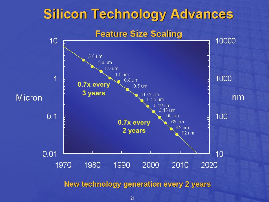
13 Semiconductor Scaling

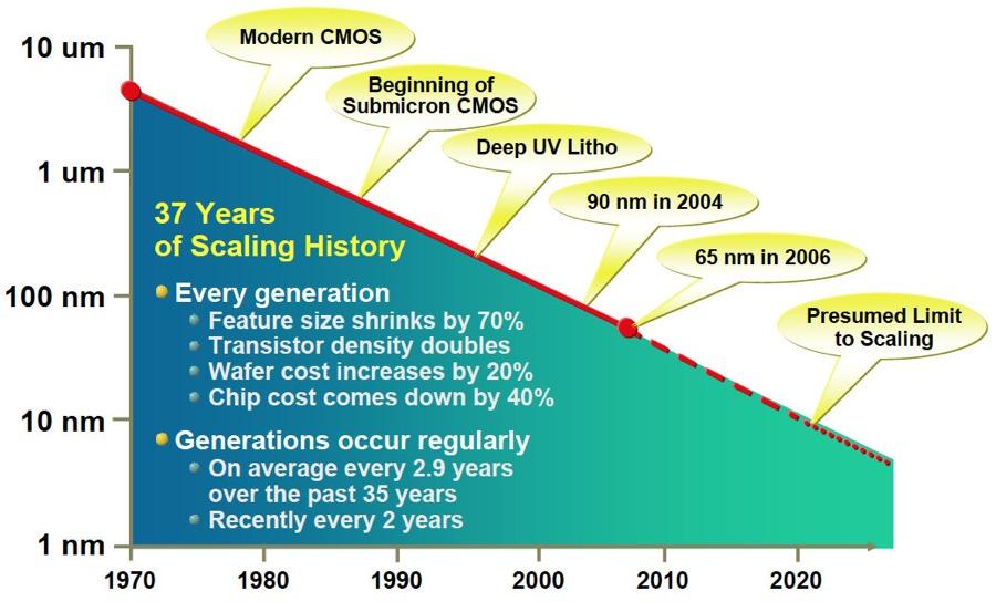
14 Processor Technology Scaling
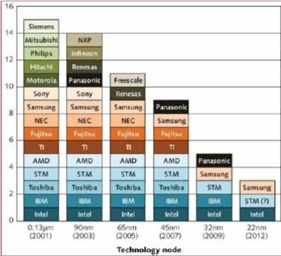
15 Technology node
16 ITRS International Technology Roadmap for Semiconductors Predictions of the worldwide semiconductor / IC industry about its own future prospects...
17 Shrinking device dimension
18 Increasing function density
19 Increasing clock frequency
20 Increasing clock frequency
21 Decreasing supply voltages
22 Moore s law on power consumption
23 Moore s law on power consumption

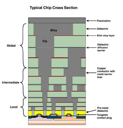
24 Cross Sectional view

25 Real Cross Sectional view

26 Type of Material Conductor Material that easily permits electrical current Eg :???? Insulator Material that block electrical current Eg :??? Semiconductor In between conductor and insulator Eg : Silicon, Germanium

27 Semiconductor vs Conductor Conductor Very easy to conduct current Behavior can t be controlled costly Semiconductor Need to do something to make it conduct behavior can be controlled cheap This is the main reason WHY SEMICONDUCTOR IS THE LEADING TECHNOLOGY NOWADAYS
28 Type of semiconductor Transistor


 terminal (generally at DC and not")
29 What is MOSFET?? Most widely used field effect transistor Let s look at its structure and physical operation 3 terminal device (gate, source, drain) Additional body (or bulk) terminal (generally at DC and not used for signals) Two types: nmos and pmos
30 nmos Transistor Four terminal device: gate, source, drain (and body) No connection between the gate and drain/source (separated by oxide) Voltage on gate controls current flow between source and drain Gate-oxide-body stack looks like a capacitor Gate and body are conductors SiO2 (oxide) is a good insulator called Metal-Oxide-Semiconductor (MOS) capacitor Gate no longer made out of metal, but poly
31 Basic nmos operation Body is commonly tied to ground (0V) When the gate is at a low voltage (VG = 0): P-type body is at low voltage Source-body and drain-body diodes are OFF (reverse bias) Depletion region between n+ and p bulk No current can flow, transistor is OFF
32 Basic nmos operation cont When the gate is at a high voltage Positive charge on gate of MOS capacitor Negative charge attracted to oxide in the body (under the gate) Inverts channel under the gate to n-type Now current can flow through this n-type channel between source and drain Transistor is ON

33 pmos Transistor Similar to nmos, but doping and voltages reversed Body tied to high voltage (Vdd) Gate low: transistor is ON inverted channel of positively charged holes Gate high: transistor is OFF Bubble indicates inverted behavior of the pmos


34 CMOS complementary-symmetry metal oxide semiconductor (CMOS) A process technology that is the basis for modern digital integrated circuits "complementary-symmetry" = uses complementary and symmetrical pairs of PMOS and NMOS for logic functions. Complementary = arrangement where the NMOS and PMOS are connected in series such that when one is on, the other is off
35 CMOS example inverter nand nor
36 Assignment =) Answer the following questions: 1. Why CMOS are more favorable than BJT? 2. What is the meaning of CMOS process technology and give some examples? 3. What is the latest CMOS process technology has been used and who was introduced that technology? 4. What is the difference between 0.18 μm CMOS process technology and 0.09 μm CMOS process technology? nm and 65 nm CMOS process technology have been introduced in the year of 2005 and 2006 respectively. Based on Moore s Law, what is the CMOS process technology expected to be introduced in 2007 and 2008
VLSI Design. Introduction
 VLSI Design Introduction Outline Introduction Silicon, pn-junctions and transistors A Brief History Operation of MOS Transistors CMOS circuits Fabrication steps for CMOS circuits Introduction Integrated
Introduction to VLSI ASIC Design and Technology
 Introduction to VLSI ASIC Design and Technology Paulo Moreira CERN - Geneva, Switzerland Paulo Moreira Introduction 1 Outline Introduction Is there a limit? Transistors CMOS building blocks Parasitics
420 Intro to VLSI Design
 Dept of Electrical and Computer Engineering 420 Intro to VLSI Design Lecture 0: Course Introduction and Overview Valencia M. Joyner Spring 2005 Getting Started Syllabus About the Instructor Labs, Problem
Progress due to: Feature size reduction - 0.7X/3 years (Moore s Law). Increasing chip size - 16% per year. Creativity in implementing functions.
. Increasing chip size - 16% per year. Creativity in implementing functions.") Introduction - Chapter 1 Evolution of IC Fabrication 1960 and 1990 integrated t circuits. it Progress due to: Feature size reduction - 0.7X/3 years (Moore s Law). Increasing chip size - 16% per year. Creativity
Introduction - Chapter 1 Evolution of IC Fabrication 1960 and 1990 integrated t circuits. it Progress due to: Feature size reduction - 0.7X/3 years (Moore s Law). Increasing chip size - 16% per year. Creativity
Lecture Integrated circuits era
 Lecture 1 1.1 Integrated circuits era Transistor was first invented by William.B.Shockley, Walter Brattain and John Bardeen of Bell laboratories. In 1961, first IC was introduced. Levels of Integration:-
VLSI Design. Introduction
 Tassadaq Hussain VLSI Design Introduction Outcome of this course Problem Aims Objectives Outcomes Data Collection Theoretical Model Mathematical Model Validate Development Analysis and Observation Pseudo
+1 (479)
") Introduction to VLSI Design http://csce.uark.edu +1 (479) 575-6043 yrpeng@uark.edu Invention of the Transistor Vacuum tubes ruled in first half of 20th century Large, expensive, power-hungry, unreliable
Introduction to VLSI Design http://csce.uark.edu +1 (479) 575-6043 yrpeng@uark.edu Invention of the Transistor Vacuum tubes ruled in first half of 20th century Large, expensive, power-hungry, unreliable
Lecture 8. MOS Transistors; Cheap Computers; Everycircuit
 Lecture 8 MOS Transistors; Cheap Computers; Everycircuit Copyright 2017 by Mark Horowitz 1 Reading The rest of Chapter 4 in the reader For more details look at A&L 5.1 Digital Signals (goes in much more
Chapter 1, Introduction
 Introduction to Semiconductor Manufacturing Technology Chapter 1, Introduction hxiao89@hotmail.com 1 Objective After taking this course, you will able to Use common semiconductor terminology Describe a
ECE 2300 Digital Logic & Computer Organization
 ECE 2300 Digital Logic & Computer Organization Spring 2018 CMOS Logic Lecture 4: 1 NAND Logic Gate X Y (X Y) = NAND Using De Morgan s Law: (X Y) = X +Y X X X +Y = Y Y Also a NAND We can build circuits
Shorthand Notation for NMOS and PMOS Transistors
 Shorthand Notation for NMOS and PMOS Transistors Terminal Voltages Mode of operation depends on V g, V d, V s V gs = V g V s V gd = V g V d V ds = V d V s = V gs - V gd Source and drain are symmetric diffusion
Integrated Circuit Technology (Course Code: EE662) Lecture 1: Introduction
 Lecture 1: Introduction") Indian Institute of Technology Jodhpur, Year 2015 2016 Integrated Circuit Technology (Course Code: EE662) Lecture 1: Introduction Course Instructor: Shree Prakash Tiwari, Ph.D. Email: sptiwari@iitj.ac.in
Indian Institute of Technology Jodhpur, Year 2015 2016 Integrated Circuit Technology (Course Code: EE662) Lecture 1: Introduction Course Instructor: Shree Prakash Tiwari, Ph.D. Email: sptiwari@iitj.ac.in
MICROPROCESSOR TECHNOLOGY
 MICROPROCESSOR TECHNOLOGY Assis. Prof. Hossam El-Din Moustafa Lecture 3 Ch.1 The Evolution of The Microprocessor 17-Feb-15 1 Chapter Objectives Introduce the microprocessor evolution from transistors to
Introduction. Reading: Chapter 1. Courtesy of Dr. Dansereau, Dr. Brown, Dr. Vranesic, Dr. Harris, and Dr. Choi.
 Introduction Reading: Chapter 1 Courtesy of Dr. Dansereau, Dr. Brown, Dr. Vranesic, Dr. Harris, and Dr. Choi http://csce.uark.edu +1 (479) 575-6043 yrpeng@uark.edu Why study logic design? Obvious reasons
EE4800 CMOS Digital IC Design & Analysis. Lecture 1 Introduction Zhuo Feng
 EE4800 CMOS Digital IC Design & Analysis Lecture 1 Introduction Zhuo Feng 1.1 Prof. Zhuo Feng Office: EERC 730 Phone: 487-3116 Email: zhuofeng@mtu.edu Class Website http://www.ece.mtu.edu/~zhuofeng/ee4800fall2010.html
Basic Fabrication Steps
 Basic Fabrication Steps and Layout Somayyeh Koohi Department of Computer Engineering Adapted with modifications from lecture notes prepared by author Outline Fabrication steps Transistor structures Transistor
ECE520 VLSI Design. Lecture 2: Basic MOS Physics. Payman Zarkesh-Ha
 ECE520 VLSI Design Lecture 2: Basic MOS Physics Payman Zarkesh-Ha Office: ECE Bldg. 230B Office hours: Wednesday 2:00-3:00PM or by appointment E-mail: pzarkesh@unm.edu Slide: 1 Review of Last Lecture Semiconductor
Digital Design and System Implementation. Overview of Physical Implementations
 Digital Design and System Implementation Overview of Physical Implementations CMOS devices CMOS transistor circuit functional behavior Basic logic gates Transmission gates Tri-state buffers Flip-flops
ECE 410: VLSI Design Course Lecture Notes (Uyemura textbook)
") ECE 410: VLSI Design Course Lecture Notes (Uyemura tetbook) Professor Fathi Salem Michigan State University We will be updating the notes this Semester. Lecture Notes Page 2.1 Electronics Revolution Age
ECE 410: VLSI Design Course Lecture Notes (Uyemura tetbook) Professor Fathi Salem Michigan State University We will be updating the notes this Semester. Lecture Notes Page 2.1 Electronics Revolution Age
Transistor was first invented by William.B.Shockley, Walter Brattain and John Bardeen of Bell Labratories. In 1961, first IC was introduced.
 Unit 1 Basic MOS Technology Transistor was first invented by William.B.Shockley, Walter Brattain and John Bardeen of Bell Labratories. In 1961, first IC was introduced. Levels of Integration:- i) SSI:-
Lecture 0: Introduction
 Lecture 0: Introduction Introduction Integrated circuits: many transistors on one chip. Very Large Scale Integration (VLSI): bucketloads! Complementary Metal Oxide Semiconductor Fast, cheap, low power
Introduction to Electronic Devices
 (Course Number 300331) Fall 2006 Instructor: Dr. Dietmar Knipp Assistant Professor of Electrical Engineering Information: http://www.faculty.iubremen.de/dknipp/ Source: Apple Ref.: Apple Ref.: IBM Critical
Digital Integrated Circuits - Logic Families (Part II)
") Digital Integrated Circuits - Logic Families (Part II) MOSFET Logic Circuits MOSFETs are unipolar devices. They are simple, small in size, inexpensive to fabricate and consume less power. MOS fabrication
Digital Integrated Circuits - Logic Families (Part II) MOSFET Logic Circuits MOSFETs are unipolar devices. They are simple, small in size, inexpensive to fabricate and consume less power. MOS fabrication
ENG2410 Digital Design CMOS Technology. Fall 2017 S. Areibi School of Engineering University of Guelph
 ENG2410 Digital Design CMOS Technology Fall 2017 S. reibi School of Engineering University of Guelph The Transistor Revolution First transistor Bell Labs, 1948 Bipolar logic 1960 s Intel 4004 processor
Lecture 4 - Digital Representations III + Transistors
 Lecture 4 - Digital Representations III + Transistors Video: Seems like a natural extension from images no? We just have a new dimension (time) Each frame is just an image made up of pixels Display n frames
INTRODUCTION TO MOS TECHNOLOGY
 INTRODUCTION TO MOS TECHNOLOGY 1. The MOS transistor The most basic element in the design of a large scale integrated circuit is the transistor. For the processes we will discuss, the type of transistor
Assoc. Prof. Dr. MONTREE SIRIPRUCHYANUN
 1 Assoc. Prof. Dr. MONTREE SIRIPRUCHYANUN Dept. of Teacher Training in Electrical Engineering 1 King Mongkut s Institute of Technology North Bangkok 1929 Bulky, expensive and required high supply voltages.
CMOS Digital Logic Design with Verilog. Chapter1 Digital IC Design &Technology
 CMOS Digital Logic Design with Verilog Chapter1 Digital IC Design &Technology Chapter Overview: In this chapter we study the concept of digital hardware design & technology. This chapter deals the standard
Semiconductor Devices
 Semiconductor Devices - 2014 Lecture Course Part of SS Module PY4P03 Dr. P. Stamenov School of Physics and CRANN, Trinity College, Dublin 2, Ireland Hilary Term, TCD 3 th of Feb 14 MOSFET Unmodified Channel
Lecture 0: Introduction
 Introduction to CMOS VLSI Design Lecture : Introduction David Harris Steven Levitan Harvey Mudd College University of Pittsburgh Spring 24 Fall 28 Administrivia Professor Steven Levitan TA: Bo Zhao Syllabus
ECE 334: Electronic Circuits Lecture 10: Digital CMOS Circuits
 Faculty of Engineering ECE 334: Electronic Circuits Lecture 10: Digital CMOS Circuits CMOS Technology Complementary MOS, or CMOS, needs both PMOS and NMOS FET devices for their logic gates to be realized
INTRODUCTION: Basic operating principle of a MOSFET:
 INTRODUCTION: Along with the Junction Field Effect Transistor (JFET), there is another type of Field Effect Transistor available whose Gate input is electrically insulated from the main current carrying
Lecture 1 Introduction to Solid State Electronics
 EE 471: Transport Phenomena in Solid State Devices Spring 2018 Lecture 1 Introduction to Solid State Electronics Bryan Ackland Department of Electrical and Computer Engineering Stevens Institute of Technology
Student Lecture by: Giangiacomo Groppi Joel Cassell Pierre Berthelot September 28 th 2004
 Student Lecture by: Giangiacomo Groppi Joel Cassell Pierre Berthelot September 28 th 2004 Lecture outline Historical introduction Semiconductor devices overview Bipolar Junction Transistor (BJT) Field
6.012 Microelectronic Devices and Circuits
 MIT, Spring 2009 6.012 Microelectronic Devices and Circuits Charles G. Sodini Jing Kong Shaya Famini, Stephanie Hsu, Ming Tang Lecture 1 6.012 Overview Contents: Overview of 6.012 Reading Assignment: Howe
CMOS VLSI IC Design. A decent understanding of all tasks required to design and fabricate a chip takes years of experience
 CMOS VLSI IC Design A decent understanding of all tasks required to design and fabricate a chip takes years of experience 1 Commonly used keywords INTEGRATED CIRCUIT (IC) many transistors on one chip VERY
VLSI: An Introduction
 Chapter 1 UEEA2223/UEEG4223 Integrated Circuit Design VLSI: An Introduction Prepared by Dr. Lim Soo King 02 Jan 2011. Chapter 1 VLSI Design: An Introduction... 1 1.0 Introduction... 1 1.0.1 Early Computing
Computer Architecture (TT 2012)
") Computer Architecture (TT 212) Laws of Attraction aniel Kroening Oxford University, Computer Science epartment Version 1., 212 . Kroening: Computer Architecture (TT 212) 2 . Kroening: Computer Architecture
Computer Architecture (TT 212) Laws of Attraction aniel Kroening Oxford University, Computer Science epartment Version 1., 212 . Kroening: Computer Architecture (TT 212) 2 . Kroening: Computer Architecture
In 1951 William Shockley developed the world first junction transistor. One year later Geoffrey W. A. Dummer published the concept of the integrated
 Objectives History and road map of integrated circuits Application specific integrated circuits Design flow and tasks Electric design automation tools ASIC project MSDAP In 1951 William Shockley developed
Spiral 1 / Unit 8. Transistor Implementations CMOS Logic Gates
 18.1 Spiral 1 / Unit 8 Transistor Implementations CMOS Logic Gates 18.2 Spiral Content Mapping Spiral Theory Combinational Design Sequential Design System Level Design Implementation and Tools Project
Jack Keil Wolf Lecture. ESE 570: Digital Integrated Circuits and VLSI Fundamentals. Lecture Outline. MOSFET N-Type, P-Type.
 ESE 570: Digital Integrated Circuits and VLSI Fundamentals Jack Keil Wolf Lecture Lec 3: January 24, 2019 MOS Fabrication pt. 2: Design Rules and Layout http://www.ese.upenn.edu/about-ese/events/wolf.php
Field-Effect Transistor (FET) is one of the two major transistors; FET derives its name from its working mechanism;
 is one of the two major transistors; FET derives its name from its working mechanism;") Chapter 3 Field-Effect Transistors (FETs) 3.1 Introduction Field-Effect Transistor (FET) is one of the two major transistors; FET derives its name from its working mechanism; The concept has been known
Chapter 3 Field-Effect Transistors (FETs) 3.1 Introduction Field-Effect Transistor (FET) is one of the two major transistors; FET derives its name from its working mechanism; The concept has been known
55:041 Electronic Circuits
 55:041 Electronic Circuits Mosfet Review Sections of Chapter 3 &4 A. Kruger Mosfet Review, Page-1 Basic Structure of MOS Capacitor Sect. 3.1 Width 1 10-6 m or less Thickness 50 10-9 m or less ` MOS Metal-Oxide-Semiconductor
Engr354: Digital Logic Circuits
 Engr354: Digital Logic Circuits Chapter 3: Implementation Technology Curtis Nelson Chapter 3 Overview In this chapter you will learn about: How transistors are used as switches; Integrated circuit technology;
CMOS Technology for Computer Architects
 CMOS Technology for Computer Architects Lecture 1: Introduction Iakovos Mavroidis Giorgos Passas Manolis Katevenis FORTH-ICS (University of Crete) Course Contents Implementation of high-performance digital
Figure.1. Schematic of 4-bit CLA JCHPS Special Issue 9: June Page 101
 Delay Depreciation and Power efficient Carry Look Ahead Adder using CMOS T. Archana*, K. Arunkumar, A. Hema Malini Department of Electronics and Communication Engineering, Saveetha Engineering College,
Lecture Introduction
 Lecture 1 6.012 Introduction 1. Overview of 6.012 Outline 2. Key conclusions of 6.012 Reading Assignment: Howe and Sodini, Chapter 1 6.012 Electronic Devices and Circuits-Fall 200 Lecture 1 1 Overview
Device Technologies. Yau - 1
 Device Technologies Yau - 1 Objectives After studying the material in this chapter, you will be able to: 1. Identify differences between analog and digital devices and passive and active components. Explain
Digital Design: An Embedded Systems Approach Using VHDL
 Digital Design: An Embedded Systems Approach Using Chapter 6 Implementation Fabrics Portions of this work are from the book, Digital Design: An Embedded Systems Approach Using, by Peter J. Ashenden, published
ESE 570: Digital Integrated Circuits and VLSI Fundamentals
 ESE 570: Digital Integrated Circuits and VLSI Fundamentals Lec 3: January 24, 2019 MOS Fabrication pt. 2: Design Rules and Layout Penn ESE 570 Spring 2019 Khanna Jack Keil Wolf Lecture http://www.ese.upenn.edu/about-ese/events/wolf.php
Introduction. Digital Integrated Circuits A Design Perspective. Jan M. Rabaey Anantha Chandrakasan Borivoje Nikolic. July 30, 2002
 Digital Integrated Circuits A Design Perspective Jan M. Rabaey Anantha Chandrakasan Borivoje Nikolic Introduction July 30, 2002 1 What is this book all about? Introduction to digital integrated circuits.
ELCN100 Electronic Lab. Instruments and Measurements Spring Lecture 01: Introduction
 ELCN100 Electronic Lab. Instruments and Measurements Spring 2018 Lecture 01: Introduction Dr. Hassan Mostafa حسن مصطفى د. hmostafa@uwaterloo.ca LAB 1 Cairo University Course Outline Course objectives To
EECS150 - Digital Design Lecture 2 - CMOS
 EECS150 - Digital Design Lecture 2 - CMOS August 29, 2002 John Wawrzynek Fall 2002 EECS150 - Lec02-CMOS Page 1 Outline Overview of Physical Implementations CMOS devices Announcements/Break CMOS transistor
2009 Spring CS211 Digital Systems & Lab 1 CHAPTER 3: TECHNOLOGY (PART 2)
") 1 CHAPTER 3: IMPLEMENTATION TECHNOLOGY (PART 2) Whatwillwelearninthischapter? we learn in this 2 How transistors operate and form simple switches CMOS logic gates IC technology FPGAs and other PLDs Basic
1 CHAPTER 3: IMPLEMENTATION TECHNOLOGY (PART 2) Whatwillwelearninthischapter? we learn in this 2 How transistors operate and form simple switches CMOS logic gates IC technology FPGAs and other PLDs Basic
EE 320 L LABORATORY 9: MOSFET TRANSISTOR CHARACTERIZATIONS. by Ming Zhu UNIVERSITY OF NEVADA, LAS VEGAS 1. OBJECTIVE 2. COMPONENTS & EQUIPMENT
 EE 320 L ELECTRONICS I LABORATORY 9: MOSFET TRANSISTOR CHARACTERIZATIONS by Ming Zhu DEPARTMENT OF ELECTRICAL AND COMPUTER ENGINEERING UNIVERSITY OF NEVADA, LAS VEGAS 1. OBJECTIVE Get familiar with MOSFETs,
Propagation Delay, Circuit Timing & Adder Design. ECE 152A Winter 2012
 Propagation Delay, Circuit Timing & Adder Design ECE 152A Winter 2012 Reading Assignment Brown and Vranesic 2 Introduction to Logic Circuits 2.9 Introduction to CAD Tools 2.9.1 Design Entry 2.9.2 Synthesis
Propagation Delay, Circuit Timing & Adder Design
 Propagation Delay, Circuit Timing & Adder Design ECE 152A Winter 2012 Reading Assignment Brown and Vranesic 2 Introduction to Logic Circuits 2.9 Introduction to CAD Tools 2.9.1 Design Entry 2.9.2 Synthesis
Module-3: Metal Oxide Semiconductor (MOS) & Emitter coupled logic (ECL) families
 & Emitter coupled logic (ECL) families") 1 Module-3: Metal Oxide Semiconductor (MOS) & Emitter coupled logic (ECL) families 1. Introduction 2. Metal Oxide Semiconductor (MOS) logic 2.1. Enhancement and depletion mode 2.2. NMOS and PMOS inverter
1 Module-3: Metal Oxide Semiconductor (MOS) & Emitter coupled logic (ECL) families 1. Introduction 2. Metal Oxide Semiconductor (MOS) logic 2.1. Enhancement and depletion mode 2.2. NMOS and PMOS inverter
Intro to Electricity. Introduction to Transistors. Example Circuit Diagrams. Water Analogy
 Introduction to Transistors Transistors form the basic building blocks of all computer hardware. Invented by William Shockley, John Bardeen and Walter Brattain in 1947, replacing previous vaccuumtube technology
ECE/CoE 0132: FETs and Gates
 ECE/CoE 0132: FETs and Gates Kartik Mohanram September 6, 2017 1 Physical properties of gates Over the next 2 lectures, we will discuss some of the physical characteristics of integrated circuits. We will
EE301 Electronics I , Fall
 EE301 Electronics I 2018-2019, Fall 1. Introduction to Microelectronics (1 Week/3 Hrs.) Introduction, Historical Background, Basic Consepts 2. Rewiev of Semiconductors (1 Week/3 Hrs.) Semiconductor materials
! Review: MOS IV Curves and Switch Model. ! MOS Device Layout. ! Inverter Layout. ! Gate Layout and Stick Diagrams. ! Design Rules. !
 ESE 570: Digital Integrated Circuits and VLSI Fundamentals Lec 3: January 21, 2017 MOS Fabrication pt. 2: Design Rules and Layout Lecture Outline! Review: MOS IV Curves and Switch Model! MOS Device Layout!
EE 42/100 Lecture 23: CMOS Transistors and Logic Gates. Rev A 4/15/2012 (10:39 AM) Prof. Ali M. Niknejad
 Prof. Ali M. Niknejad") A. M. Niknejad University of California, Berkeley EE 100 / 42 Lecture 23 p. 1/16 EE 42/100 Lecture 23: CMOS Transistors and Logic Gates ELECTRONICS Rev A 4/15/2012 (10:39 AM) Prof. Ali M. Niknejad University
A. M. Niknejad University of California, Berkeley EE 100 / 42 Lecture 23 p. 1/16 EE 42/100 Lecture 23: CMOS Transistors and Logic Gates ELECTRONICS Rev A 4/15/2012 (10:39 AM) Prof. Ali M. Niknejad University
ISSCC 2003 / SESSION 1 / PLENARY / 1.1
 ISSCC 2003 / SESSION 1 / PLENARY / 1.1 1.1 No Exponential is Forever: But Forever Can Be Delayed! Gordon E. Moore Intel Corporation Over the last fifty years, the solid-state-circuits industry has grown
55:041 Electronic Circuits
 55:041 Electronic Circuits MOSFETs Sections of Chapter 3 &4 A. Kruger MOSFETs, Page-1 Basic Structure of MOS Capacitor Sect. 3.1 Width = 1 10-6 m or less Thickness = 50 10-9 m or less ` MOS Metal-Oxide-Semiconductor
Pramoda N V Department of Electronics and Communication Engineering, MCE Hassan Karnataka India
 Advanced Low Power CMOS Design to Reduce Power Consumption in CMOS Circuit for VLSI Design Pramoda N V Department of Electronics and Communication Engineering, MCE Hassan Karnataka India Abstract: Low
FET. Field Effect Transistors ELEKTRONIKA KONTROL. Eka Maulana, ST, MT, M.Eng. Universitas Brawijaya. p + S n n-channel. Gate. Basic structure.
 FET Field Effect Transistors ELEKTRONIKA KONTROL Basic structure Gate G Source S n n-channel Cross section p + p + p + G Depletion region Drain D Eka Maulana, ST, MT, M.Eng. Universitas Brawijaya S Channel
Design cycle for MEMS
 Design cycle for MEMS Design cycle for ICs IC Process Selection nmos CMOS BiCMOS ECL for logic for I/O and driver circuit for critical high speed parts of the system The Real Estate of a Wafer MOS Transistor
UNIT III VLSI CIRCUIT DESIGN PROCESSES. In this chapter we will be studying how to get the schematic into stick diagrams or layouts.
 UNIT III VLSI CIRCUIT DESIGN PROCESSES In this chapter we will be studying how to get the schematic into stick diagrams or layouts. MOS circuits are formed on four basic layers: N-diffusion P-diffusion
EECS150 - Digital Design Lecture 15 - CMOS Implementation Technologies. Overview of Physical Implementations
 EECS150 - Digital Design Lecture 15 - CMOS Implementation Technologies Mar 12, 2013 John Wawrzynek Spring 2013 EECS150 - Lec15-CMOS Page 1 Overview of Physical Implementations Integrated Circuits (ICs)
EECS150 - Digital Design Lecture 9 - CMOS Implementation Technologies
 EECS150 - Digital Design Lecture 9 - CMOS Implementation Technologies Feb 14, 2012 John Wawrzynek Spring 2012 EECS150 - Lec09-CMOS Page 1 Overview of Physical Implementations Integrated Circuits (ICs)
EDC UNIT IV- Transistor and FET Characteristics EDC Lesson 9- ", Raj Kamal, 1
 EDC UNIT IV- Transistor and FET Characteristics Lesson-9: JFET and Construction of JFET 2008 EDC Lesson 9- ", Raj Kamal, 1 1. Transistor 2008 EDC Lesson 9- ", Raj Kamal, 2 Transistor Definition The transferred-resistance
LSI ON GLASS SUBSTRATES
 LSI ON GLASS SUBSTRATES OUTLINE Introduction: Why System on Glass? MOSFET Technology Low-Temperature Poly-Si TFT Technology System-on-Glass Technology Issues Conclusion System on Glass CPU SRAM DRAM EEPROM
6.012 Microelectronic Devices and Circuits
 MIT, Spring 2003 6.012 Microelectronic Devices and Circuits Jesús del Alamo Dimitri Antoniadis, Judy Hoyt, Charles Sodini Pablo Acosta, Susan Luschas, Jorg Scholvin, Niamh Waldron Lecture 1 6.012 overview
Homework 10 posted just for practice. Office hours next week, schedule TBD. HKN review today. Your feedback is important!
 EE141 Fall 2005 Lecture 26 Memory (Cont.) Perspectives Administrative Stuff Homework 10 posted just for practice No need to turn in Office hours next week, schedule TBD. HKN review today. Your feedback
Physics 160 Lecture 11. R. Johnson May 4, 2015
 Physics 160 Lecture 11 R. Johnson May 4, 2015 Two Solutions to the Miller Effect Putting a matching resistor on the collector of Q 1 would be a big mistake, as it would give no benefit and would produce
Introduction to Digital Logic Missouri S&T University CPE 2210 Electric Circuits
 Introduction to Digital Logic Missouri S&T University CPE 2210 Electric Circuits Egemen K. Çetinkaya Egemen K. Çetinkaya Department of Electrical & Computer Engineering Missouri University of Science and
Architecture of Computers and Parallel Systems Part 9: Digital Circuits
 Architecture of Computers and Parallel Systems Part 9: Digital Circuits Ing. Petr Olivka petr.olivka@vsb.cz Department of Computer Science FEI VSB-TUO Architecture of Computers and Parallel Systems Part
Digital Integrated Circuits
 Digital Integrated Circuits Yaping Dan ( 但亚平 ), PhD Office: Law School North 301 Tel: 34206045-3011 Email: yapingd@gmail.com Digital Integrated Circuits Introduction p-n junctions and MOSFETs The CMOS
Chapter 3: Basics Semiconductor Devices and Processing 2006/9/27 1. Topics
 Chapter 3: Basics Semiconductor Devices and Processing 2006/9/27 1 Topics What is semiconductor Basic semiconductor devices Basics of IC processing CMOS technologies 2006/9/27 2 1 What is Semiconductor
Week 7: Common-Collector Amplifier, MOS Field Effect Transistor
 EE 2110A Electronic Circuits Week 7: Common-Collector Amplifier, MOS Field Effect Transistor ecture 07-1 Topics to coer Common-Collector Amplifier MOS Field Effect Transistor Physical Operation and I-V
! Review: MOS IV Curves and Switch Model. ! MOS Device Layout. ! Inverter Layout. ! Gate Layout and Stick Diagrams. ! Design Rules. !
 ESE 570: Digital Integrated Circuits and VLSI Fundamentals Lec 3: January 21, 2016 MOS Fabrication pt. 2: Design Rules and Layout Lecture Outline! Review: MOS IV Curves and Switch Model! MOS Device Layout!
ESE 570: Digital Integrated Circuits and VLSI Fundamentals
 ESE 570: Digital Integrated Circuits and VLSI Fundamentals Lec 3: January 21, 2016 MOS Fabrication pt. 2: Design Rules and Layout Penn ESE 570 Spring 2016 Khanna Adapted from GATech ESE3060 Slides Lecture
Lecture #29. Moore s Law
 Lecture #29 ANNOUNCEMENTS HW#15 will be for extra credit Quiz #6 (Thursday 5/8) will include MOSFET C-V No late Projects will be accepted after Thursday 5/8 The last Coffee Hour will be held this Thursday
Depletion-mode operation ( 공핍형 ): Using an input gate voltage to effectively decrease the channel size of an FET
: Using an input gate voltage to effectively decrease the channel size of an FET") Ch. 13 MOSFET Metal-Oxide-Semiconductor Field-Effect Transistor : I D D-mode E-mode V g The gate oxide is made of dielectric SiO 2 with e = 3.9 Depletion-mode operation ( 공핍형 ): Using an input gate voltage
Ch. 13 MOSFET Metal-Oxide-Semiconductor Field-Effect Transistor : I D D-mode E-mode V g The gate oxide is made of dielectric SiO 2 with e = 3.9 Depletion-mode operation ( 공핍형 ): Using an input gate voltage
FPGA Based System Design
 FPGA Based System Design Reference Wayne Wolf, FPGA-Based System Design Pearson Education, 2004 Why VLSI? Integration improves the design: higher speed; lower power; physically smaller. Integration reduces
ECE 340 Lecture 37 : Metal- Insulator-Semiconductor FET Class Outline:
 ECE 340 Lecture 37 : Metal- Insulator-Semiconductor FET Class Outline: Metal-Semiconductor Junctions MOSFET Basic Operation MOS Capacitor Things you should know when you leave Key Questions What is the
Chapter 2 : Semiconductor Materials & Devices (II) Feb
 Feb") Chapter 2 : Semiconductor Materials & Devices (II) 1 Reference 1. SemiconductorManufacturing Technology: Michael Quirk and Julian Serda (2001) 3. Microelectronic Circuits (5/e): Sedra & Smith (2004) 4.
Chapter 2 : Semiconductor Materials & Devices (II) 1 Reference 1. SemiconductorManufacturing Technology: Michael Quirk and Julian Serda (2001) 3. Microelectronic Circuits (5/e): Sedra & Smith (2004) 4.
ECE 5745 Complex Digital ASIC Design Topic 2: CMOS Devices
 ECE 5745 Complex Digital ASIC Design Topic 2: CMOS Devices Christopher Batten School of Electrical and Computer Engineering Cornell University http://www.csl.cornell.edu/courses/ece5950 Simple Transistor
Intel s High-k/Metal Gate Announcement. November 4th, 2003
 Intel s High-k/Metal Gate Announcement November 4th, 2003 1 What are we announcing? Intel has made significant progress in future transistor materials Two key parts of this new transistor are: The gate
Silicon VLSI Technology. Fundamentals, Practice and Modeling. Class Notes For Instructors. J. D. Plummer, M. D. Deal and P. B.
 Silicon VLSI Technology Fundamentals, ractice, and Modeling Class otes For Instructors J. D. lummer, M. D. Deal and. B. Griffin These notes are intended to be used for lectures based on the above text.
12-nm Novel Topologies of LPHP: Low-Power High- Performance 2 4 and 4 16 Mixed-Logic Line Decoders
 12-nm Novel Topologies of LPHP: Low-Power High- Performance 2 4 and 4 16 Mixed-Logic Line Decoders Mr.Devanaboina Ramu, M.tech Dept. of Electronics and Communication Engineering Sri Vasavi Institute of
Metal-Oxide-Silicon (MOS) devices PMOS. n-type
 devices PMOS. n-type") Metal-Oxide-Silicon (MOS devices Principle of MOS Field Effect Transistor transistor operation Metal (poly gate on oxide between source and drain Source and drain implants of opposite type to substrate.
Metal-Oxide-Silicon (MOS devices Principle of MOS Field Effect Transistor transistor operation Metal (poly gate on oxide between source and drain Source and drain implants of opposite type to substrate.
Lecture 1, Introduction and Background
 EE 338L CMOS Analog Integrated Circuit Design Lecture 1, Introduction and Background With the advances of VLSI (very large scale integration) technology, digital signal processing is proliferating and
Chapter 3 Digital Logic Structures
 Chapter 3 Digital Logic Structures Transistor: Building Block of Computers Microprocessors contain millions of transistors Intel Pentium 4 (2000): 48 million IBM PowerPC 750FX (2002): 38 million IBM/Apple
Integrated diodes. The forward voltage drop only slightly depends on the forward current. ELEKTRONIKOS ĮTAISAI
 1 Integrated diodes pn junctions of transistor structures can be used as integrated diodes. The choice of the junction is limited by the considerations of switching speed and breakdown voltage. The forward
Chapter 3 Basics Semiconductor Devices and Processing
 Chapter 3 Basics Semiconductor Devices and Processing 1 Objectives Identify at least two semiconductor materials from the periodic table of elements List n-type and p-type dopants Describe a diode and
TECHNO INDIA BATANAGAR (DEPARTMENT OF ELECTRONICS & COMMUNICATION ENGINEERING) QUESTION BANK- 2018
 QUESTION BANK- 2018") TECHNO INDIA BATANAGAR (DEPARTMENT OF ELECTRONICS & COMMUNICATION ENGINEERING) QUESTION BANK- 2018 Paper Setter Detail Name Designation Mobile No. E-mail ID Raina Modak Assistant Professor 6290025725 raina.modak@tib.edu.in
TECHNO INDIA BATANAGAR (DEPARTMENT OF ELECTRONICS & COMMUNICATION ENGINEERING) QUESTION BANK- 2018 Paper Setter Detail Name Designation Mobile No. E-mail ID Raina Modak Assistant Professor 6290025725 raina.modak@tib.edu.in
Chapter 1. Introduction
 EECS3611 Analog Integrated Circuit esign Chapter 1 Introduction EECS3611 Analog Integrated Circuit esign Instructor: Prof. Ebrahim Ghafar-Zadeh, Prof. Peter Lian email: egz@cse.yorku.ca peterlian@cse.yorku.ca
PHYSICAL STRUCTURE OF CMOS INTEGRATED CIRCUITS. Dr. Mohammed M. Farag
 PHYSICAL STRUCTURE OF CMOS INTEGRATED CIRCUITS Dr. Mohammed M. Farag Outline Integrated Circuit Layers MOSFETs CMOS Layers Designing FET Arrays EE 432 VLSI Modeling and Design 2 Integrated Circuit Layers