Fundamentals of CMOS Image Sensors
|
|
|
- Egbert Greer
- 6 years ago
- Views:
Transcription

1 CHAPTER 2 Fundamentals of CMOS Image Sensors Mixed-Signal IC Design for Image Sensor 2-1
2 Outline Photoelectric Effect Photodetectors CMOS Image Sensor(CIS) Array Architecture CIS Peripherals Design Considerations Evaluations of Image Sensors Mixed-Signal IC Design for Image Sensor 2-2
3 Outline Photoelectric Effect Photodetectors CMOS Image Sensor(CIS) Array Architecture CIS Peripherals Design Considerations Evaluations of Image Sensors Mixed-Signal IC Design for Image Sensor 2-3

4 Architecture of a CIS Mixed-Signal IC Design for Image Sensor 2-4

5 Photo-generated Carriers The amount of photo-generated carriers - Depends on the semiconductor material - Described by the absorption coefficient α Mixed-Signal IC Design for Image Sensor 2-5
6 Absorption Coefficient Absorption coefficient α Absorption length L abs Visible light (0.4 ~ 0.6um) L abs 0.1~10um Mixed-Signal IC Design for Image Sensor 2-6

7 α : Depends on Material Mixed-Signal IC Design for Image Sensor 2-7
8 Behavior of Minority Carriers Large absorption length of IR Photo-generated minority carrier in substrate Long life time & diffusion Crosstalk Need IR cut filter to suppress blur effect Mixed-Signal IC Design for Image Sensor 2-8
9 Diffusion Length vs. Impurity Conc. Diffusion lengths > 10um with concentration < 1E18cm -3 Mixed-Signal IC Design for Image Sensor 2-9
10 Quantum Efficiency and Sensitivity Sensitivity I L : Photocurrent, P 0 : unit light power Quantum efficiency # of generated carrier / # of input photons Maximum sensitivity (at η Q = 1) Mixed-Signal IC Design for Image Sensor 2-10
11 Sensitivity of Silicon Mixed-Signal IC Design for Image Sensor 2-11

12 Quantum Efficiency and Sensitivity Light intensity PN-junction structure Mixed-Signal IC Design for Image Sensor 2-12

13 Quantum efficiency Sensitivity Mixed-Signal IC Design for Image Sensor 2-13
14 QE: Dotted Sensitivity : Solid Mixed-Signal IC Design for Image Sensor 2-14

15 QE in P-N Junction Mixed-Signal IC Design for Image Sensor 2-

16 QE in P-N Junction Mixed-Signal IC Design for Image Sensor 2-

17 Structures of PDs, PGs, and PTrs. photogate photodiode V-phototransistor L-phototransistor Mixed-Signal IC Design for Image Sensor 2-17
18 Forward current PN Junction Diode Photocurrent of the pn-junction PD Mixed-Signal IC Design for Image Sensor 2-18
19 PD I V Curves Mixed-Signal IC Design for Image Sensor 2-19
20 Solar cell mode (get V oc from I L =0) PD mode (reverse biased ) Avalanche mode - Used in an avalanche photodiode (APD) : single photon detection Mixed-Signal IC Design for Image Sensor 2-20

21 Dark Current G R current (generation-recombination) Thermal generation Diffusion current Minority diffusion Surface leak current Si-SiO 2 interface Mixed-Signal IC Design for Image Sensor 2-
22 Dark Current Diffusion current T I diff Tunnel current - Band-to-band tunneling (BTBT) - Trap-assisted tunneling (TAT) Mixed-Signal IC Design for Image Sensor 2-22
23 Dark Current G R current (generation-recombination) Thermal generation Surface leak current Mixed-Signal IC Design for Image Sensor 2-23
24 Surface Recombination SiO 2 interfaces the surface of the silicon Produce surface states or interface states Carriers near the surface are trapped Degrade the quantum efficiency or sensitivity (critical for short wavelength light) Mixed-Signal IC Design for Image Sensor 2-
25 Dependence of I dark (T, V) Mixed-Signal IC Design for Image Sensor 2-25
26 Temporal Noise Shot noise Signal-to-noise ratio (SNR) for shot noise Mixed-Signal IC Design for Image Sensor 2-26
27 Temporal Noise Thermal noise - Johnson noise or Nyquist noise - Appears as ktc noise Mixed-Signal IC Design for Image Sensor 2-27

28 Spatial Noise Fixed Pattern Noise (FPN) Pixel uniformity Readout circuit uniformity Array FPN Column FPN Mixed-Signal IC Design for Image Sensor 2-28
29 Photon Transfer Curve Mixed-Signal IC Design for Image Sensor 2-29
30 Speed Some kinds of smart image sensors need a PD with a fast response - for optical wireless LANs - measure time-of-flight (TOF) Mixed-Signal IC Design for Image Sensor 2-30
31 The response of a PD is limited by (1) CR time constant (2) Transit time (3) Diffusion time of minority carriers Mixed-Signal IC Design for Image Sensor 2-31
32 Outline Photoelectric Effect Photodetectors CMOS Image Sensor(CIS) Array Architecture CIS Peripherals Design Considerations Evaluations of Image Sensors Mixed-Signal IC Design for Image Sensor 2-32
33 Photogate Mixed-Signal IC Design for Image Sensor 2-33
34 Phototransistor Amplifies a photocurrent by a factor of the base current gain β - Not high, typically about Large variation ( produces FPN ) When base width increases, the quantum efficiency increases but the gain decreases Mixed-Signal IC Design for Image Sensor 2-34
35 Avalanche Photodiode (APD) High-speed response Optical fiber communication Ultra low light detection (single photon) Spike-current output (not for imaging) Require a high voltage over 100 V Low voltage operation possibility at sub-micron technology Mixed-Signal IC Design for Image Sensor 2-35
36 Avalanche Photodiode Structure Mixed-Signal IC Design for Image Sensor 2-36
37 Photoconductive Detector (PCD) Typically has a structure of n + n n + Gain originates from two parts - Long lifetime of holes τ p - Short transit time of electrons t tr Mixed-Signal IC Design for Image Sensor 2-37
38 MSM Photodetector Metal-Semiconductor-Metal (MSM) Photodetector A kind of PCD Easy to fabricate Ultra-fast photodetectors (GaAs MSM) Image sensors with a sensitivity in the UV region (GaN MSM) Mixed-Signal IC Design for Image Sensor 2-38

39 Structure of MSM Photodetector Mixed-Signal IC Design for Image Sensor 2-39
40 Outline Photoelectric Effect Photodetectors CMOS Image Sensor(CIS) Array Architecture CIS Peripherals Design Considerations Evaluations of Image Sensors Mixed-Signal IC Design for Image Sensor 2-40
41 Architecture of a CIS Mixed-Signal IC Design for Image Sensor 2-41
42 Active & Passive Pixel Mixed-Signal IC Design for Image Sensor 2-42
43 Active & Passive Pixel Mixed-Signal IC Design for Image Sensor 2-43
44 Accumulation Mode Electrical floating PD as capacitor Accumulation of photo-generated carrier is interpreted as discharge process. R ph = 0.3A/W, PD area A = 100um 2, illumination L o = 100lux, 1lux~= 1.6x10⁻⁷ W/cm 2 Accumulation is necessary at video rate Mixed-Signal IC Design for Image Sensor 2-44
45 Accumulation Mode Junction capacitance (depends on applied bias V) For C PD (V) : linearly proportional to I ph + I d Mixed-Signal IC Design for Image Sensor 2-45
46 Voltage Drop of a PD Mixed-Signal IC Design for Image Sensor 2-46
47 Potential Description Mixed-Signal IC Design for Image Sensor 2-47
48 Mixed-Signal IC Design for Image Sensor 2-48
49 Behavior of Carriers in PD Mixed-Signal IC Design for Image Sensor 2-49
50 Pinned Photodiode (PPD) Also buried photodiode (BPD) Has less dark current than a conventional PD Has an accumulation region with complete depletion Need precise fabrication process control Mixed-Signal IC Design for Image Sensor 2-50

51 Photo-Generated Carriers in PPD Mixed-Signal IC Design for Image Sensor 2-51

52 Passive Pixel Sensor Advantages - very simple - large fill factor (FF) Disadvantages - large smear (?) - large k B TC noise - large column FPN Mixed-Signal IC Design for Image Sensor 2-52

53 On-Chip Column Amplifier Gain loss due to large C C Mixed-Signal IC Design for Image Sensor 2-53
 k B TC noise is reduced Little switching noise Mixed-Signal IC Design for")
54 Transversal Signal Line (TSL) Drastically reduces smear (?) k B TC noise is reduced Little switching noise Mixed-Signal IC Design for Image Sensor 2-54


55 Active Pixel Sensor, 3T-APS Basic pixel circuits of a 3T-APS Mixed-Signal IC Design for Image Sensor 2-55
56 Issues with 3T-APS It is difficult to suppress k B TC noise PD simultaneously acts as a photo conversion region. This constrains the PD design Full-well capacity and the conversion gain have a trade-off relationship Mixed-Signal IC Design for Image Sensor 2-56


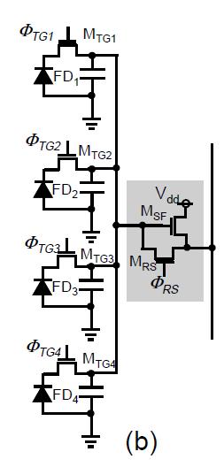
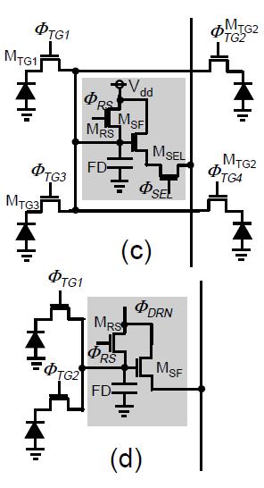
57 Active Pixel Sensor, 4T-APS Basic pixel circuits of the 4T-APS Mixed-Signal IC Design for Image Sensor 2-57
58 Issues with 4T-APS The additional transistor reduces the FF Image lag may occur when the accumulated signal charge is completely transferred into the FD It is difficult to establish fabrication process parameters Mixed-Signal IC Design for Image Sensor 2-58
59 Incomplete Charge Transfer Mixed-Signal IC Design for Image Sensor 2-59
60 Outline Photoelectric Effect Photodetectors CMOS Image Sensor(CIS) Array Architecture CIS Peripherals Design Considerations Evaluations of Image Sensors Mixed-Signal IC Design for Image Sensor 2-60

61 Addressing scanner decoder Mixed-Signal IC Design for Image Sensor 2-61

62 Typical method Random Access Mixed-Signal IC Design for Image Sensor 2-62

63 Random Access A different types of random access Mixed-Signal IC Design for Image Sensor 2-63

64 Source follower Readout Circuits Mixed-Signal IC Design for Image Sensor 2-64
65 Correlated Double Sampling (CDS) Eliminate the threshold mismatch (FPN) of readout path Eliminate thermal (ktc) noise from reset transistor Mixed-Signal IC Design for Image Sensor 2-65
66 3T CDS (with ktc noise) Mixed-Signal IC Design for Image Sensor 2-66
67 4T CDS (no ktc noise) Mixed-Signal IC Design for Image Sensor 2-67

68 Alternative CDS Mixed-Signal IC Design for Image Sensor 2-68

69 CDS with Differential Output Typical circuitry for CDS with a 4T-APS pixel circuit Mixed-Signal IC Design for Image Sensor 2-69
70 Timing chart of CDS Mixed-Signal IC Design for Image Sensor 2-70
71 4T Differential Delta Sampling (DDS) Mixed-Signal IC Design for Image Sensor 2-71
72 Rolling Shutter Mixed-Signal IC Design for Image Sensor 2-72
73 Shape Distortion Mixed-Signal IC Design for Image Sensor 2-73
74 Mechanical Shutter (Rolling Rst) Mixed-Signal IC Design for Image Sensor 2-74
75 Mechanical Shutter (Global Rst) Mixed-Signal IC Design for Image Sensor 2-75
76 Electronic Global Shutter Mixed-Signal IC Design for Image Sensor 2-76
77 Mode Change & Dead Frame Mixed-Signal IC Design for Image Sensor 2-77

78 Sub-Resolution Mixed-Signal IC Design for Image Sensor 2-78
79 Pixel Binning Mixed-Signal IC Design for Image Sensor 2-79
80 Analog Front End Mixed-Signal IC Design for Image Sensor 2-80
81 Analog-to-Digital Converters Chip-shared structure Pipelined ADC Flash ADC Column parallel structure Single slope ADC Successive approximation ADC Cyclic ADC Delta-Sigma ADC Mixed-Signal IC Design for Image Sensor 2-81
82 Outline Photoelectric Effect Photodetectors CMOS Image Sensor(CIS) Array Architecture CIS Peripherals Design Considerations Evaluations of Image Sensors Mixed-Signal IC Design for Image Sensor 2-82
83 Reset Noise k B TC noise Mixed-Signal IC Design for Image Sensor 2-83
84 Reset Method Soft reset - V PD slowly reaches V dd V th - Image lag Hard reset - gate voltage is larger than V dd - reset action finishes quickly - k B TC noise Mixed-Signal IC Design for Image Sensor 2-84

85 Flushed Reset Hard reset first Then soft reset to reduce k B TC noise Mixed-Signal IC Design for Image Sensor 2-85
86 Dynamic Range The ratio of the maximum signal range to the minimum signal range Determined by two factors Noise floor (min.) Well charge capacity (max.) DR Full Well Charge 20log( Noise floor ) Mixed-Signal IC Design for Image Sensor 2-86
87 Color Reproduction There are three ways to realize color in a conventional CMOS image sensor - On-chip color filter type - Three imagers type - Three light sources type Mixed-Signal IC Design for Image Sensor 2-87

88 On-chip Color Filter Type Three colored filters are directly placed on the pixels - RGB or CMY complementary color filters Mixed-Signal IC Design for Image Sensor 2-88
89 Three Imagers Type High color fidelity Complicated optics Expensive Mixed-Signal IC Design for Image Sensor 2-89

90 Three Light Sources Type Mainly used in medical endoscopes Color fidelity is excellent Time to acquire a whole image is long Mixed-Signal IC Design for Image Sensor 2-90

91 Multiple Junction Pixel Mixed-Signal IC Design for Image Sensor 2-91

92 Pixel Sharing Mixed-Signal IC Design for Image Sensor 2-92

93 Zigzag Placement of RGB Pixels Mixed-Signal IC Design for Image Sensor 2-93
94 Comparison of Pixels Mixed-Signal IC Design for Image Sensor 2-94
95 Outline Photoelectric Effect Photodetectors CMOS Image Sensor(CIS) Array Architecture CIS Peripherals Design Considerations Evaluations of Image Sensors Mixed-Signal IC Design for Image Sensor 2-95
96 Evaluation Items Mixed-Signal IC Design for Image Sensor 2-96

97 Evaluation Environment Mixed-Signal IC Design for Image Sensor 2-97

98 Factors of Environment Light Source Imaging Lens Optical Filter Alignment Temperature Evaluation board Mixed-Signal IC Design for Image Sensor 2-98
99 Evaluation Methods Dark Characteristic Average dark current Temporal noise FPN (DSNU) Illuminated Characteristic Response Linearity Sensitivity Saturation SNR (Dynamic range) FPN (PRNU) Mixed-Signal IC Design for Image Sensor 2-99
100 Spectral Response Angular Response Smear Resolution Image Lag Defects Evaluation Methods Mixed-Signal IC Design for Image Sensor 2-100
101 Photoconversion Mixed-Signal IC Design for Image Sensor 2-101
102 Linear Saturation Mixed-Signal IC Design for Image Sensor 2-102

103 Dark FPN Measurement Mixed-Signal IC Design for Image Sensor 2-103
104 Spectral Response Mixed-Signal IC Design for Image Sensor 2-104


105 Incident Light Angle Control Mixed-Signal IC Design for Image Sensor 2-105

106 Angular Response Mixed-Signal IC Design for Image Sensor 2-106
107 Image Lag Measurement Mixed-Signal IC Design for Image Sensor 2-107
Photons and solid state detection
 Photons and solid state detection Photons represent discrete packets ( quanta ) of optical energy Energy is hc/! (h: Planck s constant, c: speed of light,! : wavelength) For solid state detection, photons
Detectors for Optical Communications
 Optical Communications: Circuits, Systems and Devices Chapter 3: Optical Devices for Optical Communications lecturer: Dr. Ali Fotowat Ahmady Sep 2012 Sharif University of Technology 1 Photo All detectors
Optical Receivers Theory and Operation
 Optical Receivers Theory and Operation Photo Detectors Optical receivers convert optical signal (light) to electrical signal (current/voltage) Hence referred O/E Converter Photodetector is the fundamental
Lecture 18: Photodetectors
 Lecture 18: Photodetectors Contents 1 Introduction 1 2 Photodetector principle 2 3 Photoconductor 4 4 Photodiodes 6 4.1 Heterojunction photodiode.................... 8 4.2 Metal-semiconductor photodiode................
EE 392B: Course Introduction
 EE 392B Course Introduction About EE392B Goals Topics Schedule Prerequisites Course Overview Digital Imaging System Image Sensor Architectures Nonidealities and Performance Measures Color Imaging Recent
Application of CMOS sensors in radiation detection
 Application of CMOS sensors in radiation detection S. Ashrafi Physics Faculty University of Tabriz 1 CMOS is a technology for making low power integrated circuits. CMOS Complementary Metal Oxide Semiconductor
Ultra-high resolution 14,400 pixel trilinear color image sensor
 Ultra-high resolution 14,400 pixel trilinear color image sensor Thomas Carducci, Antonio Ciccarelli, Brent Kecskemety Microelectronics Technology Division Eastman Kodak Company, Rochester, New York 14650-2008
E19 PTC and 4T APS. Cristiano Rocco Marra 20/12/2017
 POLITECNICO DI MILANO MSC COURSE - MEMS AND MICROSENSORS - 2017/2018 E19 PTC and 4T APS Cristiano Rocco Marra 20/12/2017 In this class we will introduce the photon transfer tecnique, a commonly-used routine
14.2 Photodiodes 411
 14.2 Photodiodes 411 Maximum reverse voltage is specified for Ge and Si photodiodes and photoconductive cells. Exceeding this voltage can cause the breakdown and severe deterioration of the sensor s performance.
Chap14. Photodiode Detectors
 Chap14. Photodiode Detectors Mohammad Ali Mansouri-Birjandi mansouri@ece.usb.ac.ir mamansouri@yahoo.com Faculty of Electrical and Computer Engineering University of Sistan and Baluchestan (USB) Design
Active Pixel Sensors Fabricated in a Standard 0.18 um CMOS Technology
 Active Pixel Sensors Fabricated in a Standard.18 um CMOS Technology Hui Tian, Xinqiao Liu, SukHwan Lim, Stuart Kleinfelder, and Abbas El Gamal Information Systems Laboratory, Stanford University Stanford,
Photodiode: LECTURE-5
 LECTURE-5 Photodiode: Photodiode consists of an intrinsic semiconductor sandwiched between two heavily doped p-type and n-type semiconductors as shown in Fig. 3.2.2. Sufficient reverse voltage is applied
OPTOELECTRONIC and PHOTOVOLTAIC DEVICES
 OPTOELECTRONIC and PHOTOVOLTAIC DEVICES Outline 1. Introduction to the (semiconductor) physics: energy bands, charge carriers, semiconductors, p-n junction, materials, etc. 2. Light emitting diodes Light
Three Ways to Detect Light. We now establish terminology for photon detectors:
 Three Ways to Detect Light In photon detectors, the light interacts with the detector material to produce free charge carriers photon-by-photon. The resulting miniscule electrical currents are amplified
Part I. CCD Image Sensors
 Part I CCD Image Sensors 2 Overview of CCD CCD is the abbreviation for charge-coupled device. CCD image sensors are silicon-based integrated circuits (ICs), consisting of a dense matrix of photodiodes
Optical Amplifiers. Continued. Photonic Network By Dr. M H Zaidi
 Optical Amplifiers Continued EDFA Multi Stage Designs 1st Active Stage Co-pumped 2nd Active Stage Counter-pumped Input Signal Er 3+ Doped Fiber Er 3+ Doped Fiber Output Signal Optical Isolator Optical
Optical Communications
 Optical Communications Telecommunication Engineering School of Engineering University of Rome La Sapienza Rome, Italy 2005-2006 Lecture #4, May 9 2006 Receivers OVERVIEW Photodetector types: Photodiodes
Optical Fiber Communication Lecture 11 Detectors
 Optical Fiber Communication Lecture 11 Detectors Warriors of the Net Detector Technologies MSM (Metal Semiconductor Metal) PIN Layer Structure Semiinsulating GaAs Contact InGaAsP p 5x10 18 Absorption InGaAs
Lecture 8 Optical Sensing. ECE 5900/6900 Fundamentals of Sensor Design
 ECE 5900/6900: Fundamentals of Sensor Design Lecture 8 Optical Sensing 1 Optical Sensing Q: What are we measuring? A: Electromagnetic radiation labeled as Ultraviolet (UV), visible, or near,mid-, far-infrared
Characterization of CMOS Image Sensor
 Characterization of CMOS Image Sensor Master of Science Thesis For the degree of Master of Science in Microelectronics at Delft University of Technology Utsav Jain July 21,2016 Faculty of Electrical Engineering,
Charge coupled CMOS and hybrid detector arrays
 Charge coupled CMOS and hybrid detector arrays James Janesick Sarnoff Corporation, 4952 Warner Ave., Suite 300, Huntington Beach, CA. 92649 Headquarters: CN5300, 201 Washington Road Princeton, NJ 08543-5300
Lecture 9 External Modulators and Detectors
 Optical Fibres and Telecommunications Lecture 9 External Modulators and Detectors Introduction Where are we? A look at some real laser diodes. External modulators Mach-Zender Electro-absorption modulators
Detectors for microscopy - CCDs, APDs and PMTs. Antonia Göhler. Nov 2014
 Detectors for microscopy - CCDs, APDs and PMTs Antonia Göhler Nov 2014 Detectors/Sensors in general are devices that detect events or changes in quantities (intensities) and provide a corresponding output,
Trend of CMOS Imaging Device Technologies
 004 6 ( ) CMOS : Trend of CMOS Imaging Device Technologies 3 7110 Abstract Which imaging device survives in the current fast-growing and competitive market, imagers or CMOS imagers? Although this question
Silicon sensors for radiant signals. D.Sc. Mikko A. Juntunen
 Silicon sensors for radiant signals D.Sc. Mikko A. Juntunen 2017 01 16 Today s outline Introduction Basic physical principles PN junction revisited Applications Light Ionizing radiation X-Ray sensors in
STA1600LN x Element Image Area CCD Image Sensor
 ST600LN 10560 x 10560 Element Image Area CCD Image Sensor FEATURES 10560 x 10560 Photosite Full Frame CCD Array 9 m x 9 m Pixel 95.04mm x 95.04mm Image Area 100% Fill Factor Readout Noise 2e- at 50kHz
Simulation of High Resistivity (CMOS) Pixels
 Pixels") Simulation of High Resistivity (CMOS) Pixels Stefan Lauxtermann, Kadri Vural Sensor Creations Inc. AIDA-2020 CMOS Simulation Workshop May 13 th 2016 OUTLINE 1. Definition of High Resistivity Pixel Also
Simulation of High Resistivity (CMOS) Pixels Stefan Lauxtermann, Kadri Vural Sensor Creations Inc. AIDA-2020 CMOS Simulation Workshop May 13 th 2016 OUTLINE 1. Definition of High Resistivity Pixel Also
Based on lectures by Bernhard Brandl
 Astronomische Waarneemtechnieken (Astronomical Observing Techniques) Based on lectures by Bernhard Brandl Lecture 10: Detectors 2 1. CCD Operation 2. CCD Data Reduction 3. CMOS devices 4. IR Arrays 5.
ACTIVE PIXEL SENSORS VS. CHARGE-COUPLED DEVICES
 ACTIVE PIXEL SENSORS VS. CHARGE-COUPLED DEVICES Dr. Eric R. Fossum Imaging Systems Section Jet Propulsion Laboratory, California Institute of Technology (818) 354-3128 1993 IEEE Workshop on CCDs and Advanced
OFCS OPTICAL DETECTORS 11/9/2014 LECTURES 1
 OFCS OPTICAL DETECTORS 11/9/2014 LECTURES 1 1-Defintion & Mechanisms of photodetection It is a device that converts the incident light into electrical current External photoelectric effect: Electrons are
CMOS Today & Tomorrow
 CMOS Today & Tomorrow Uwe Pulsfort TDALSA Product & Application Support Overview Image Sensor Technology Today Typical Architectures Pixel, ADCs & Data Path Image Quality Image Sensor Technology Tomorrow
A 3MPixel Multi-Aperture Image Sensor with 0.7µm Pixels in 0.11µm CMOS
 A 3MPixel Multi-Aperture Image Sensor with 0.7µm Pixels in 0.11µm CMOS Keith Fife, Abbas El Gamal, H.-S. Philip Wong Stanford University, Stanford, CA Outline Introduction Chip Architecture Detailed Operation
Engineering Medical Optics BME136/251 Winter 2018
 Engineering Medical Optics BME136/251 Winter 2018 Monday/Wednesday 2:00-3:20 p.m. Beckman Laser Institute Library, MSTB 214 (lab) *1/17 UPDATE Wednesday, 1/17 Optics and Photonic Devices III: homework
Characterization of CMOS Image Sensor
 Characterization of CMOS Image Sensor Master of Science Thesis For the degree of Master of Science in Microelectronics at Delft University of Technology Utsav Jain August 31, 2016 Faculty of Electrical
A flexible compact readout circuit for SPAD arrays ABSTRACT Keywords: 1. INTRODUCTION 2. THE SPAD 2.1 Operation 7780C - 55
 A flexible compact readout circuit for SPAD arrays Danial Chitnis * and Steve Collins Department of Engineering Science University of Oxford Oxford England OX13PJ ABSTRACT A compact readout circuit that
FUTURE PROSPECTS FOR CMOS ACTIVE PIXEL SENSORS
 FUTURE PROSPECTS FOR CMOS ACTIVE PIXEL SENSORS Dr. Eric R. Fossum Jet Propulsion Laboratory Dr. Philip H-S. Wong IBM Research 1995 IEEE Workshop on CCDs and Advanced Image Sensors April 21, 1995 CMOS APS
CCDS. Lesson I. Wednesday, August 29, 12
 CCDS Lesson I CCD OPERATION The predecessor of the CCD was a device called the BUCKET BRIGADE DEVICE developed at the Phillips Research Labs The BBD was an analog delay line, made up of capacitors such
Figure Responsivity (A/W) Figure E E-09.
 Figure E E-09.") OSI Optoelectronics, is a leading manufacturer of fiber optic components for communication systems. The products offer range for Silicon, GaAs and InGaAs to full turnkey solutions. Photodiodes are semiconductor
OSI Optoelectronics, is a leading manufacturer of fiber optic components for communication systems. The products offer range for Silicon, GaAs and InGaAs to full turnkey solutions. Photodiodes are semiconductor
Department of Electrical Engineering IIT Madras
 Department of Electrical Engineering IIT Madras Sample Questions on Semiconductor Devices EE3 applicants who are interested to pursue their research in microelectronics devices area (fabrication and/or
Performance and Characteristics of Silicon Avalanche Photodetectors in
 Performance and Characteristics of Silicon Avalanche Photodetectors in the C5 Process Paper Authors: Dennis Montierth 1, Timothy Strand 2, James Leatham 2, Lloyd Linder 3, and R. Jacob Baker 1 1 Dept.
MOSFET MODULATED DUAL CONVERSION GAIN CMOS IMAGE SENSORS
 MOSFET MODULATED DUAL CONVERSION GAIN CMOS IMAGE SENSORS By Xiangli Li A dissertation submitted in partial fulfillment of the requirements for the degree of Doctor of Philosophy in Electrical and Computer
CCD1600A Full Frame CCD Image Sensor x Element Image Area
 - 1 - General Description CCD1600A Full Frame CCD Image Sensor 10560 x 10560 Element Image Area General Description The CCD1600 is a 10560 x 10560 image element solid state Charge Coupled Device (CCD)
A High Image Quality Fully Integrated CMOS Image Sensor
 A High Image Quality Fully Integrated CMOS Image Sensor Matt Borg, Ray Mentzer and Kalwant Singh Hewlett-Packard Company, Corvallis, Oregon Abstract We describe the feature set and noise characteristics
Charged Coupled Device (CCD) S.Vidhya
 S.Vidhya") Charged Coupled Device (CCD) S.Vidhya 02.04.2016 Sensor Physical phenomenon Sensor Measurement Output A sensor is a device that measures a physical quantity and converts it into a signal which can be read
Charged Coupled Device (CCD) S.Vidhya 02.04.2016 Sensor Physical phenomenon Sensor Measurement Output A sensor is a device that measures a physical quantity and converts it into a signal which can be read
Figure Figure E E-09. Dark Current (A) 1.
 1.") OSI Optoelectronics, is a leading manufacturer of fiber optic components for communication systems. The products offer range for Silicon, GaAs and InGaAs to full turnkey solutions. Photodiodes are semiconductor
OSI Optoelectronics, is a leading manufacturer of fiber optic components for communication systems. The products offer range for Silicon, GaAs and InGaAs to full turnkey solutions. Photodiodes are semiconductor
CMOS Active Pixel Sensor Technology for High Performance Machine Vision Applications
 CMOS Active Pixel Sensor Technology for High Performance Machine Vision Applications Nicholas A. Doudoumopoulol Lauren Purcell 1, and Eric R. Fossum 2 1Photobit, LLC 2529 Foothill Blvd. Suite 104, La Crescenta,
Where detectors are used in science & technology
 Lecture 9 Outline Role of detectors Photomultiplier tubes (photoemission) Modulation transfer function Photoconductive detector physics Detector architecture Where detectors are used in science & technology
Jan Bogaerts imec
 imec 2007 1 Radiometric Performance Enhancement of APS 3 rd Microelectronic Presentation Days, Estec, March 7-8, 2007 Outline Introduction Backside illuminated APS detector Approach CMOS APS (readout)
Computational Sensors
 Computational Sensors Suren Jayasuriya Postdoctoral Fellow, The Robotics Institute, Carnegie Mellon University Class Announcements 1) Vote on this poll about project checkpoint date on Piazza: https://piazza.com/class/j6dobp76al46ao?cid=126
Automotive Image Sensors
 Automotive Image Sensors February 1st 2018 Boyd Fowler and Johannes Solhusvik 1 Outline Automotive Image Sensor Market and Applications Viewing Sensors HDR Flicker Mitigation Machine Vision Sensors In
Demonstration of a Frequency-Demodulation CMOS Image Sensor
 Demonstration of a Frequency-Demodulation CMOS Image Sensor Koji Yamamoto, Keiichiro Kagawa, Jun Ohta, Masahiro Nunoshita Graduate School of Materials Science, Nara Institute of Science and Technology
Introduction to silicon photomultipliers (SiPMs) White paper
 White paper") Introduction to silicon photomultipliers (SiPMs) White paper Basic structure and operation The silicon photomultiplier (SiPM) is a radiation detector with extremely high sensitivity, high efficiency, and
Introduction to silicon photomultipliers (SiPMs) White paper Basic structure and operation The silicon photomultiplier (SiPM) is a radiation detector with extremely high sensitivity, high efficiency, and
Lecture 14: Photodiodes
 Lecture 14: Photodiodes Background concepts p-n photodiodes photoconductive/photovoltaic modes p-i-n photodiodes responsivity and bandwidth Reading: Senior 8.1-8.8.3 Keiser Chapter 6 1 Electron-hole photogeneration
Design and Simulation of N-Substrate Reverse Type Ingaasp/Inp Avalanche Photodiode
 International Refereed Journal of Engineering and Science (IRJES) ISSN (Online) 2319-183X, (Print) 2319-1821 Volume 2, Issue 8 (August 2013), PP.34-39 Design and Simulation of N-Substrate Reverse Type
10/14/2009. Semiconductor basics pn junction Solar cell operation Design of silicon solar cell
 PHOTOVOLTAICS Fundamentals PV FUNDAMENTALS Semiconductor basics pn junction Solar cell operation Design of silicon solar cell SEMICONDUCTOR BASICS Allowed energy bands Valence and conduction band Fermi
ELEN6350. Summary: High Dynamic Range Photodetector Hassan Eddrees, Matt Bajor
 ELEN6350 High Dynamic Range Photodetector Hassan Eddrees, Matt Bajor Summary: The use of image sensors presents several limitations for visible light spectrometers. Both CCD and CMOS one dimensional imagers
Problem 4 Consider a GaAs p-n + junction LED with the following parameters at 300 K: Electron diusion coecient, D n = 25 cm 2 =s Hole diusion coecient
 Prof. Jasprit Singh Fall 2001 EECS 320 Homework 7 This homework is due on November 8. Problem 1 An optical power density of 1W/cm 2 is incident on a GaAs sample. The photon energy is 2.0 ev and there is
What is the highest efficiency Solar Cell?
 What is the highest efficiency Solar Cell? GT CRC Roof-Mounted PV System Largest single PV structure at the time of it s construction for the 1996 Olympic games Produced more than 1 billion watt hrs. of
ABSTRACT. Section I Overview of the µdss
 An Autonomous Low Power High Resolution micro-digital Sun Sensor Ning Xie 1, Albert J.P. Theuwissen 1, 2 1. Delft University of Technology, Delft, the Netherlands; 2. Harvest Imaging, Bree, Belgium; ABSTRACT
DIGITAL IMAGING. Handbook of. Wiley VOL 1: IMAGE CAPTURE AND STORAGE. Editor-in- Chief
 Handbook of DIGITAL IMAGING VOL 1: IMAGE CAPTURE AND STORAGE Editor-in- Chief Adjunct Professor of Physics at the Portland State University, Oregon, USA Previously with Eastman Kodak; University of Rochester,
Semiconductor Physics and Devices
 Metal-Semiconductor and Semiconductor Heterojunctions The Metal-Oxide-Semiconductor Field-Effect Transistor (MOSFET) is one of two major types of transistors. The MOSFET is used in digital circuit, because
Chapter 3 OPTICAL SOURCES AND DETECTORS
 Chapter 3 OPTICAL SOURCES AND DETECTORS 3. Optical sources and Detectors 3.1 Introduction: The success of light wave communications and optical fiber sensors is due to the result of two technological breakthroughs.
Recent Development and Study of Silicon Solid State Photomultiplier (MRS Avalanche Photodetector)
") Recent Development and Study of Silicon Solid State Photomultiplier (MRS Avalanche Photodetector) Valeri Saveliev University of Obninsk, Russia Vienna Conference on Instrumentation Vienna, 20 February
Recent Development and Study of Silicon Solid State Photomultiplier (MRS Avalanche Photodetector) Valeri Saveliev University of Obninsk, Russia Vienna Conference on Instrumentation Vienna, 20 February
Design and Performance of a Pinned Photodiode CMOS Image Sensor Using Reverse Substrate Bias
 Design and Performance of a Pinned Photodiode CMOS Image Sensor Using Reverse Substrate Bias 13 September 2017 Konstantin Stefanov Contents Background Goals and objectives Overview of the work carried
Introduction. Chapter 1
 1 Chapter 1 Introduction During the last decade, imaging with semiconductor devices has been continuously replacing conventional photography in many areas. Among all the image sensors, the charge-coupled-device
Semiconductor Detector Systems
 Semiconductor Detector Systems Helmuth Spieler Physics Division, Lawrence Berkeley National Laboratory OXFORD UNIVERSITY PRESS ix CONTENTS 1 Detector systems overview 1 1.1 Sensor 2 1.2 Preamplifier 3
Characterization of CMOS Image Sensors with Nyquist Rate Pixel Level ADC
 Characterization of CMOS Image Sensors with Nyquist Rate Pixel Level ADC David Yang, Hui Tian, Boyd Fowler, Xinqiao Liu, and Abbas El Gamal Information Systems Laboratory, Stanford University, Stanford,
Photon Count. for Brainies.
 Page 1/12 Photon Count ounting for Brainies. 0. Preamble This document gives a general overview on InGaAs/InP, APD-based photon counting at telecom wavelengths. In common language, telecom wavelengths
Dynamic Range. Can I look at bright and faint things at the same time?
 Detector Basics The purpose of any detector is to record the light collected by the telescope. All detectors transform the incident radiation into a some other form to create a permanent record, such as
Development of the Pixelated Photon Detector. Using Silicon on Insulator Technology. for TOF-PET
 July 24, 2015 Development of the Pixelated Photon Detector Using Silicon on Insulator Technology for TOF-PET A.Koyama 1, K.Shimazoe 1, H.Takahashi 1, T. Orita 2, Y.Arai 3, I.Kurachi 3, T.Miyoshi 3, D.Nio
More Imaging Luc De Mey - CEO - CMOSIS SA
 More Imaging Luc De Mey - CEO - CMOSIS SA Annual Review / June 28, 2011 More Imaging CMOSIS: Vision & Mission CMOSIS s Business Concept On-Going R&D: More Imaging CMOSIS s Vision Image capture is a key
FEATURES GENERAL DESCRIPTION. CCD Element Linear Image Sensor CCD Element Linear Image Sensor
 CCD 191 6000 Element Linear Image Sensor FEATURES 6000 x 1 photosite array 10µm x 10µm photosites on 10µm pitch Anti-blooming and integration control Enhanced spectral response (particularly in the blue
LEDs, Photodetectors and Solar Cells
 LEDs, Photodetectors and Solar Cells Chapter 7 (Parker) ELEC 424 John Peeples Why the Interest in Photons? Answer: Momentum and Radiation High electrical current density destroys minute polysilicon and
Solar Cell Parameters and Equivalent Circuit
 9 Solar Cell Parameters and Equivalent Circuit 9.1 External solar cell parameters The main parameters that are used to characterise the performance of solar cells are the peak power P max, the short-circuit
Chapter 3 Wide Dynamic Range & Temperature Compensated Gain CMOS Image Sensor in Automotive Application. 3.1 System Architecture
 Chapter 3 Wide Dynamic Range & Temperature Compensated Gain CMOS Image Sensor in Automotive Application Like the introduction said, we can recognize the problem would be suffered on image sensor in automotive
UNIT VIII-SPECIAL PURPOSE ELECTRONIC DEVICES. 1. Explain tunnel Diode operation with the help of energy band diagrams.
 UNIT III-SPECIAL PURPOSE ELECTRONIC DEICES 1. Explain tunnel Diode operation with the help of energy band diagrams. TUNNEL DIODE: A tunnel diode or Esaki diode is a type of semiconductor diode which is
Lecture 7. July 24, Detecting light (converting light to electrical signal)
") Lecture 7 July 24, 2017 Detecting light (converting light to electrical signal) Photoconductor Photodiode Managing electrical signal Metal-oxide-semiconductor (MOS) capacitor Charge coupled device (CCD)
Lecture 7 July 24, 2017 Detecting light (converting light to electrical signal) Photoconductor Photodiode Managing electrical signal Metal-oxide-semiconductor (MOS) capacitor Charge coupled device (CCD)
Semiconductor Devices Lecture 5, pn-junction Diode
 Semiconductor Devices Lecture 5, pn-junction Diode Content Contact potential Space charge region, Electric Field, depletion depth Current-Voltage characteristic Depletion layer capacitance Diffusion capacitance
OPTI510R: Photonics. Khanh Kieu College of Optical Sciences, University of Arizona Meinel building R.626
 OPTI510R: Photonics Khanh Kieu College of Optical Sciences, University of Arizona kkieu@optics.arizona.edu Meinel building R.626 Photodetectors Introduction Most important characteristics Photodetector
STA3600A 2064 x 2064 Element Image Area CCD Image Sensor
 ST600A 2064 x 2064 Element Image Area CCD Image Sensor FEATURES 2064 x 2064 CCD Image Array 15 m x 15 m Pixel 30.96 mm x 30.96 mm Image Area Near 100% Fill Factor Readout Noise Less Than 3 Electrons at
Device design for global shutter operation in a 1.1-um pixel image sensor and its application to nearinfrared
 Device design for global shutter operation in a 1.1-um pixel image sensor and its application to nearinfrared sensing Zach M. Beiley Robin Cheung Erin F. Hanelt Emanuele Mandelli Jet Meitzner Jae Park
PRELIMINARY. CCD 3041 Back-Illuminated 2K x 2K Full Frame CCD Image Sensor FEATURES
 CCD 3041 Back-Illuminated 2K x 2K Full Frame CCD Image Sensor FEATURES 2048 x 2048 Full Frame CCD 15 µm x 15 µm Pixel 30.72 mm x 30.72 mm Image Area 100% Fill Factor Back Illuminated Multi-Pinned Phase
Unit 2 Semiconductor Devices. Lecture_2.5 Opto-Electronic Devices
 Unit 2 Semiconductor Devices Lecture_2.5 Opto-Electronic Devices Opto-electronics Opto-electronics is the study and application of electronic devices that interact with light. Electronics (electrons) Optics
Camera Test Protocol. Introduction TABLE OF CONTENTS. Camera Test Protocol Technical Note Technical Note
 Technical Note CMOS, EMCCD AND CCD CAMERAS FOR LIFE SCIENCES Camera Test Protocol Introduction The detector is one of the most important components of any microscope system. Accurate detector readings
EVALUATION OF RADIATION HARDNESS DESIGN TECHNIQUES TO IMPROVE RADIATION TOLERANCE FOR CMOS IMAGE SENSORS DEDICATED TO SPACE APPLICATIONS
 EVALUATION OF RADIATION HARDNESS DESIGN TECHNIQUES TO IMPROVE RADIATION TOLERANCE FOR CMOS IMAGE SENSORS DEDICATED TO SPACE APPLICATIONS P. MARTIN-GONTHIER, F. CORBIERE, N. HUGER, M. ESTRIBEAU, C. ENGEL,
Cameras CS / ECE 181B
 Cameras CS / ECE 181B Image Formation Geometry of image formation (Camera models and calibration) Where? Radiometry of image formation How bright? What color? Examples of cameras What is a Camera? A camera
Overview. Charge-coupled Devices. MOS capacitor. Charge-coupled devices. Charge-coupled devices:
 Overview Charge-coupled Devices Charge-coupled devices: MOS capacitors Charge transfer Architectures Color Limitations 1 2 Charge-coupled devices MOS capacitor The most popular image recording technology
Three Ways to Detect Light. Following: Lord Rosse image of M33 vs. Hubble image demonstrate how critical detector technology is.
 Three Ways to Detect Light In photon detectors, the light interacts with the detector material to produce free charge carriers photon-by-photon. The resulting miniscule electrical currents are amplified
IT FR R TDI CCD Image Sensor
 4k x 4k CCD sensor 4150 User manual v1.0 dtd. August 31, 2015 IT FR 08192 00 R TDI CCD Image Sensor Description: With the IT FR 08192 00 R sensor ANDANTA GmbH builds on and expands its line of proprietary
LAB V. LIGHT EMITTING DIODES
 LAB V. LIGHT EMITTING DIODES 1. OBJECTIVE In this lab you are to measure I-V characteristics of Infrared (IR), Red and Blue light emitting diodes (LEDs). The emission intensity as a function of the diode
The market for solid-state image sensors
 Abbas El Gamal and Helmy Eltoukhy The market for solid-state image sensors has been experiencing explosive growth in recent years due to the increasing demands of mobile imaging, digital still and video
UNIT III. By Ajay Kumar Gautam Asst. Prof. Electronics & Communication Engineering Dev Bhoomi Institute of Technology & Engineering, Dehradun
 UNIT III By Ajay Kumar Gautam Asst. Prof. Electronics & Communication Engineering Dev Bhoomi Institute of Technology & Engineering, Dehradun SYLLABUS Optical Absorption in semiconductors, Types of Photo
1 Introduction & Motivation 1
 Abstract Just five years ago, digital cameras were considered a technological luxury appreciated by only a few, and it was said that digital image quality would always lag behind that of conventional film
Functional Materials. Optoelectronic devices
 Functional Materials Lecture 2: Optoelectronic materials and devices (inorganic). Photonic materials Optoelectronic devices Light-emitting diode (LED) displays Photodiode and Solar cell Photoconductive
FIBER OPTICS. Prof. R.K. Shevgaonkar. Department of Electrical Engineering. Indian Institute of Technology, Bombay. Lecture: 20
 FIBER OPTICS Prof. R.K. Shevgaonkar Department of Electrical Engineering Indian Institute of Technology, Bombay Lecture: 20 Photo-Detectors and Detector Noise Fiber Optics, Prof. R.K. Shevgaonkar, Dept.
Design of an Integrated Image Sensor System
 Institute of Integrated Sensor Systems Dept. of Electrical Engineering and Information Technology Design of an Integrated Image Sensor System Kuan Shang Fall Semester, 2007 Prof. Dr.-Ing. Andreas König
CONTENTS. 2.2 Schrodinger's Wave Equation 31. PART I Semiconductor Material Properties. 2.3 Applications of Schrodinger's Wave Equation 34
 CONTENTS Preface x Prologue Semiconductors and the Integrated Circuit xvii PART I Semiconductor Material Properties CHAPTER 1 The Crystal Structure of Solids 1 1.0 Preview 1 1.1 Semiconductor Materials
KAF E. 512(H) x 512(V) Pixel. Enhanced Response. Full-Frame CCD Image Sensor. Performance Specification. Eastman Kodak Company
 x 512(V) Pixel. Enhanced Response. Full-Frame CCD Image Sensor. Performance Specification. Eastman Kodak Company") KAF - 0261E 512(H) x 512(V) Pixel Enhanced Response Full-Frame CCD Image Sensor Performance Specification Eastman Kodak Company Image Sensor Solutions Rochester, New York 14650 Revision 2 December 21,
KAF - 0261E 512(H) x 512(V) Pixel Enhanced Response Full-Frame CCD Image Sensor Performance Specification Eastman Kodak Company Image Sensor Solutions Rochester, New York 14650 Revision 2 December 21,
Avalanche Photodiode. Instructor: Prof. Dietmar Knipp Presentation by Peter Egyinam. 4/19/2005 Photonics and Optical communicaton
 Avalanche Photodiode Instructor: Prof. Dietmar Knipp Presentation by Peter Egyinam 1 Outline Background of Photodiodes General Purpose of Photodiodes Basic operation of p-n, p-i-n and avalanche photodiodes
Key Questions ECE 340 Lecture 28 : Photodiodes
 Things you should know when you leave Key Questions ECE 340 Lecture 28 : Photodiodes Class Outline: How do the I-V characteristics change with illumination? How do solar cells operate? How do photodiodes