Photonic Crystal Slot Waveguide Spectrometer for Detection of Methane
|
|
|
- Lenard Bates
- 6 years ago
- Views:
Transcription

1 Photonic Crystal Slot Waveguide Spectrometer for Detection of Methane Swapnajit Chakravarty 1, Wei-Cheng Lai 2, Xiaolong (Alan) Wang 1, Che-Yun Lin 2, Ray T. Chen 1,2 1 Omega Optics, Sausalito Drive, Austin, TX Dept. of Electrical and Computer Engineering, University of Texas, Austin Funded by Environmental Protection Agency (EPA) SBIR Grant #: EP-D


 FTIR Spectroscopy (24lbs, ~ 1.5cu.")
 10 µm 300 µm Photonic Crystal Slot")
2 Motivation No other chip based optical method for infrared molecular absorption spectroscopy of gases Tunable Diode Laser Absorption Spectroscopy Our Device Cavity Ringdown Spectroscopy (66lbs, ~ 3cu.ft) FTIR Spectroscopy (24lbs, ~ 1.5cu.ft,) Photoacoustic Spectroscopy (33lbs, ~ 1cu.ft) 10 µm 300 µm Photonic Crystal Slot Waveguide Spectrometer (< 0.1 lbs, <10cu. cm.) 2
3 What is Photonic Crystal? Periodic electromagnetic media comparable to wavelength With photonic band gaps: optical insulators 1-D grating =1-D PhC 2-D PhC =2-D grating 3-D PhC =3-D grating Similar to: Semiconductors Defect structures can introduce defect mode inside the photonic bandgap Similar to: Doping of Semiconductor can trap light in cavities and waveguides ( wires ) 3D Pho to nic C rysta l with De fe c ts 3

, 4648 (2003) Ion Sensing Chakravarty et al, Optics Lett.")

4 Photonic Crystal Bio-Chemical Sensors Sensing principle based on change in refractive index Chemical Sensing Loncar et al, Appl. Phys. Lett. 82 (26), 4648 (2003) Ion Sensing Chakravarty et al, Optics Lett. 30 (19), 2578 (2005) Frontiers in Biological Detection: From Nanosensors to Systems, Conference 7888, SPIE Photonics West 2011 Bio-Sensing Lee et al, Optics Exp. 15 (8), 4530 (2007) 4
5 Photonic Crystal Slot Waveguide Spectroscopy Principle is based on Beer-Lambert absorption law: I = I 0 exp[ γαl] where I =Transmitted Intensity at the output of photonic crystal slot waveguide at wavelength λ I 0 = Incident Optical power at wavelength λ L = Geometrical optical path length = 300µm γ = Medium-specific absorption factor determined by dispersion enhanced light-matter interaction α = Absorption coefficient at wavelength λ γ = f c / n where c =Velocity of light in medium of refractive index n. v g = Group velocity of light in the photonic crystal waveguide f = Electric field intensity enhancement in the slot v g Mortensen et al, Appl. Phys. Lett. 90 (14), (2007) 5


6 Photonic Crystal Waveguide W-1 PCW Normalized dispersion diagram Scaled in wavelength by scaling the lattice constant of the photonic crystal 6


7 Photonic Crystal Slot Waveguide Photonic crystal period a=460nm Waveguide height h=0.5a Hole diameter d=0.5a Slot width w 0 =0.2a Defect width w 1 =1.3 a Slot Enhancement Advantages: Slow photon group velocity Smaller mode profile Compatible fabrication processes with silicon photonics Xu et al, Optics Lett (2004) 7


8 Photonic Crystal Slot Waveguide Design Device Parameters on a SOI wafer Guided mode design in SOI wafer Factor of 12 enhancement in slot with mode 3. Designed for wavelength at which mode 3 has group index n g =40, which coincides with the peak of the near-infrared absorption spectrum of methane at nm. 8

9 Device Fabrication Steps Standard silicon fabrication steps Thermal Oxide Growth Resist Patterning Silicon Dioxide Hard Mask Pattern transferred to Silicon Structures considered with bottom SiO 2 cladding for mechanical stability for operation in harsh environments Minimum feature sizes easily achievable by 193nm photolithography 9

10 Photonic Crystal Slot Waveguide Slot in the middle of a photonic crystal waveguide Mode Converter for higher coupling efficiency from the ridge waveguide into slot Photonic Crystal Impedance Taper for higher coupling efficiency into slow light region 10


11 Methods to improve Optical Coupling Efficiency n 0 =3.5<n 1 <n 2 < <n k-1 <n k =100 Group index varied gradually by shifting the edge air holes; from low group index at the ridge waveguide to high group index at the photonic crystal waveguide slow light regime. Xiaolong Wang, Ray T. Chen, Photonic Crystal Band-Shifting Device for Dynamic Control of Light Transmission, U.S. patent 455,791 (2009) 11


12 Experimental Setup Light is guided in and out of the photonic crystal waveguide by optical fibers Light propagates in direction perpendicular to flow of fluid Sample cell for controlled environment during experiments; not required for final product 12
 Experimentally, n g ~30; Slot enhancement ~12 More than an order of magnitude higher sensitivity can be achieved with wavelength/frequency modulation spectroscopy in near-ir (1ppm), on")
13 Methane Detection in N 2 Ambient by Spectroscopy At 1.665µm, detection sensitivity of methane achieved for a 300µm long photonic crystal slot waveguide= 100ppm =0.03ppm-m (=0.2% PEL) Experimentally, n g ~30; Slot enhancement ~12 More than an order of magnitude higher sensitivity can be achieved with wavelength/frequency modulation spectroscopy in near-ir (1ppm), on chip-integrated platform 13
14 Requirements from Gas Sensors Property Requirement Photonic Crystal Slot Waveguide Spectroscopy Cost < $50/unit for single gas CH 4 sensor Detection Sensitivity Device Reusability / Longevity Cross-Talk / False Positives/ Specificity High volume manufacturing in on-chip CMOS platform (< $20) <1% of LEL (500ppm for CH 4 ) Function of absorption cross-section (~40ppm Near-IR, ~400ppb Mid-IR) 5 years without recalibration or ~12 hours if battery-operated Minimum interference from other substances with signatures in similar wavelengths Sensitivity sufficient for most practical purposes No electronic components, longevity determined by silicon Specificity achieved by multiple detection on-chip More than an order of magnitude higher sensitivity can be achieved with wavelength/frequency modulation spectroscopy in near-ir (1ppm), on chip-integrated platform Absorbance cross-sections in mid-ir are 2 orders of magnitude larger (10ppb), on chipintegrated platform 14
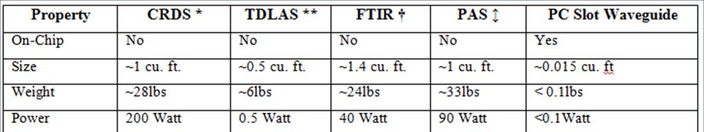
15 Comparison with other Technologies 15
16 Summary Photonic crystal Absorption spectrometers enable: Very low cost of ownership Sensitivity sufficient for most practical purposes Generous deployment of sensors in field Multiple species detection on-chip Less chance for false positives Small size enables minimum interference with existing processes In-situ detection and remote monitoring Application Areas : Industrial process gas monitoring & quality control Air quality control & monitoring (Greenhouse and Hazardous Gases) Explosives detection 16
17 Discussion: Minimum Detectable Sensitivity Smallest number density that can be determined by absorption spectroscopy di N min = ( ) / S( ν ) L I where di/i 0 = smallest fractional change in light intensity that can be detected = L = effective absorption path length = 300µm 1000= 30cm S(ν) =absorption cross section of methane at 1.665µm = cm 2 [HITRAN] N min = per cm 3 0 At 1.665µm, detection limit of methane for a 300µm long photonic crystal slot waveguide= 40ppm (=0.15% LEL) Experimentally, n g ~30; Slot enhancement ~12 Experimentally detected: 100ppm =0.03ppm-m 17
Computer Engineering, University of Texas, Burnet Road Bldg. 160, Austin, TX USA ABSTRACT 1. INTRODUCTION 2. PRINCIPLE OF OPERATION
 Photonic crystal slot waveguide Spectrometer for detection of Methane Swapnajit Chakravarty* a, Wei-Cheng Lai b, Xiaolong Wang a, Cheyun Lin b, Ray T. Chen b, a Omega Optics Inc., 10306 Sausalito Drive,
160MER, Austin, TX-78758, USA ABSTRACT 1. INTRODUCTION
 Group velocity independent coupling into slow light photonic crystal waveguide on silicon nanophotonic integrated circuits Che-Yun Lin* a, Xiaolong Wang a, Swapnajit Chakravarty b, Wei-Cheng Lai a, Beom
Omega Optics Inc., 8500 Shoal Creek Blvd., Austin, TX ABSTRACT 1. INTRODUCTION
 Integrated strip and slot waveguides in silicon-on-sapphire for Mid Infrared VOC detection in Water Yi Zou, 1,* Harish Subbaraman, 2 Swapnajit Chakravarty, 2,* Xiaochuan Xu, 2 Amir Hosseini, 2 Wei- Cheng
Miniature Mid-Infrared Thermooptic Switch with Photonic Crystal Waveguide Based Silicon-on-Sapphire Mach Zehnder Interferometers
 Miniature Mid-Infrared Thermooptic Switch with Photonic Crystal Waveguide Based Silicon-on- Mach Zehnder Interferometers Yi Zou, 1,* Swapnajit Chakravarty, 2,* Chi-Jui Chung, 1 1, 2, * and Ray T. Chen
2D silicon-based surface-normal vertical cavity photonic crystal waveguide array for high-density optical interconnects
 2D silicon-based surface-normal vertical cavity photonic crystal waveguide array for high-density optical interconnects JaeHyun Ahn a, Harish Subbaraman b, Liang Zhu a, Swapnajit Chakravarty b, Emanuel
CHAPTER 2 POLARIZATION SPLITTER- ROTATOR BASED ON A DOUBLE- ETCHED DIRECTIONAL COUPLER
 CHAPTER 2 POLARIZATION SPLITTER- ROTATOR BASED ON A DOUBLE- ETCHED DIRECTIONAL COUPLER As we discussed in chapter 1, silicon photonics has received much attention in the last decade. The main reason is
20dB-enhanced coupling to slot photonic crystal waveguide based on. multimode interference
 20dB-enhanced coupling to slot photonic crystal waveguide based on multimode interference Xiaonan Chen 1, Lanlan Gu 2, Wei Jiang 2, and Ray T. Chen 1* Microelectronic Research Center, Department of Electrical
Examination Optoelectronic Communication Technology. April 11, Name: Student ID number: OCT1 1: OCT 2: OCT 3: OCT 4: Total: Grade:
 Examination Optoelectronic Communication Technology April, 26 Name: Student ID number: OCT : OCT 2: OCT 3: OCT 4: Total: Grade: Declaration of Consent I hereby agree to have my exam results published on
Characterization of Photonic Structures with CST Microwave Studio. CST UGM 2010 Darmstadt
 Characterization of Photonic Structures with CST Microwave Studio Stefan Prorok, Jan Hendrik Wülbern, Jan Hampe, Hooi Sing Lee, Alexander Petrov and Manfred Eich, Institute of Optical and Electronic Materials
Waveguiding in PMMA photonic crystals
 ROMANIAN JOURNAL OF INFORMATION SCIENCE AND TECHNOLOGY Volume 12, Number 3, 2009, 308 316 Waveguiding in PMMA photonic crystals Daniela DRAGOMAN 1, Adrian DINESCU 2, Raluca MÜLLER2, Cristian KUSKO 2, Alex.
Optics Communications
 Optics Communications 283 (2010) 3678 3682 Contents lists available at ScienceDirect Optics Communications journal homepage: www.elsevier.com/locate/optcom Ultra-low-loss inverted taper coupler for silicon-on-insulator
 Chapter 5 5.1 What are the factors that determine the thickness of a polystyrene waveguide formed by spinning a solution of dissolved polystyrene onto a substrate? density of polymer concentration of polymer
Impact of the light coupling on the sensing properties of photonic crystal cavity modes Kumar Saurav* a,b, Nicolas Le Thomas a,b,
 Impact of the light coupling on the sensing properties of photonic crystal cavity modes Kumar Saurav* a,b, Nicolas Le Thomas a,b, a Photonics Research Group, Ghent University-imec, Technologiepark-Zwijnaarde
Waveguide Bragg Gratings and Resonators LUMERICAL SOLUTIONS INC
 Waveguide Bragg Gratings and Resonators JUNE 2016 1 Outline Introduction Waveguide Bragg gratings Background Simulation challenges and solutions Photolithography simulation Initial design with FDTD Band
Extreme Sensitivity in Photoacoustics by Using Optical Cantilever-type Microphone
 Extreme Sensitivity in Photoacoustics by Using Optical Cantilever-type Microphone Jyrki Kauppinen, Vesa Koskinen, Minna Huuskonen Department of Physics, University of Turku, FIN-20014 TURKU, Finland, e-mail:
Two bit optical analog-to-digital converter based on photonic crystals
 Two bit optical analog-to-digital converter based on photonic crystals Binglin Miao, Caihua Chen, Ahmed Sharkway, Shouyuan Shi, and Dennis W. Prather University of Delaware, Newark, Delaware 976 binglin@udel.edu
Experimental demonstration of propagation characteristics of mid-infrared photonic crystal waveguides in silicon-on-sapphire
 Experimental demonstration of propagation characteristics of mid-infrared photonic crystal waveguides in silicon-on-sapphire Yi Zou, 1,4,* Swapnajit Chakravarty, 2,3,4 Parker Wray, 1 and Ray T. Chen 1,2,5
CHIRPED FIBER BRAGG GRATING (CFBG) BY ETCHING TECHNIQUE FOR SIMULTANEOUS TEMPERATURE AND REFRACTIVE INDEX SENSING
 BY ETCHING TECHNIQUE FOR SIMULTANEOUS TEMPERATURE AND REFRACTIVE INDEX SENSING") CHIRPED FIBER BRAGG GRATING (CFBG) BY ETCHING TECHNIQUE FOR SIMULTANEOUS TEMPERATURE AND REFRACTIVE INDEX SENSING Siti Aisyah bt. Ibrahim and Chong Wu Yi Photonics Research Center Department of Physics,
CHIRPED FIBER BRAGG GRATING (CFBG) BY ETCHING TECHNIQUE FOR SIMULTANEOUS TEMPERATURE AND REFRACTIVE INDEX SENSING Siti Aisyah bt. Ibrahim and Chong Wu Yi Photonics Research Center Department of Physics,
Micro-sensors - what happens when you make "classical" devices "small": MEMS devices and integrated bolometric IR detectors
 Micro-sensors - what happens when you make "classical" devices "small": MEMS devices and integrated bolometric IR detectors Dean P. Neikirk 1 MURI bio-ir sensors kick-off 6/16/98 Where are the targets
Introduction Fundamentals of laser Types of lasers Semiconductor lasers
 ECE 5368 Introduction Fundamentals of laser Types of lasers Semiconductor lasers Introduction Fundamentals of laser Types of lasers Semiconductor lasers How many types of lasers? Many many depending on
Optical behavior. Reading assignment. Topic 10
 Reading assignment Optical behavior Topic 10 Askeland and Phule, The Science and Engineering of Materials, 4 th Ed.,Ch. 0. Shackelford, Materials Science for Engineers, 6 th Ed., Ch. 16. Chung, Composite
10/14/2009. Semiconductor basics pn junction Solar cell operation Design of silicon solar cell
 PHOTOVOLTAICS Fundamentals PV FUNDAMENTALS Semiconductor basics pn junction Solar cell operation Design of silicon solar cell SEMICONDUCTOR BASICS Allowed energy bands Valence and conduction band Fermi
Optodevice Data Book ODE I. Rev.9 Mar Opnext Japan, Inc.
 Optodevice Data Book ODE-408-001I Rev.9 Mar. 2003 Opnext Japan, Inc. Section 1 Operating Principles 1.1 Operating Principles of Laser Diodes (LDs) and Infrared Emitting Diodes (IREDs) 1.1.1 Emitting Principles
Physics of Waveguide Photodetectors with Integrated Amplification
 Physics of Waveguide Photodetectors with Integrated Amplification J. Piprek, D. Lasaosa, D. Pasquariello, and J. E. Bowers Electrical and Computer Engineering Department University of California, Santa
Luminous Equivalent of Radiation
 Intensity vs λ Luminous Equivalent of Radiation When the spectral power (p(λ) for GaP-ZnO diode has a peak at 0.69µm) is combined with the eye-sensitivity curve a peak response at 0.65µm is obtained with
High dynamic range electric field sensor for electromagnetic pulse detection
 High dynamic range electric field sensor for electromagnetic pulse detection Che-Yun Lin, 1,3 Alan X. Wang, 2,3 Beom Suk Lee, 1 Xingyu Zhang, 1 and Ray T. Chen 1,* 1 Microelectronics Research Center, The
Wide Absorption Spectrum Measuring Methods by DFB-LDs in Water Vapor Detection System
 PHOTONIC SENSORS / Vol. 4, No. 3, 2014: 230 235 Wide Absorption Spectrum Measuring Methods by DFB-LDs in Water Vapor Detection System Y. N. LIU 1, J. CHANG 1*, J. LIAN 1, Q. WANG 1, G. P. LV 1, W. J. WANG
High Resolution and Wide Dynamic Range Pressure Sensor Based on Two-Dimensional Photonic Crystal
 (212) Vol. 2, No. 1: 92 96 DOI: 17/s12-11-44-1 Regular High Resolution and Wide Dynamic Range Pressure Sensor Based on Two-Dimensional Photonic Crystal Saeed OLYAEE and Ali Asghar DEHGHANI Nano-photonics
Ultra-Compact Photonic Crystal Based Water Temperature Sensor
 PHOTONIC SENSORS / Vol. 6, No. 3, 2016: 274 278 Ultra-Compact Photonic Crystal Based Water Temperature Sensor Mahmoud NIKOUFARD *, Masoud KAZEMI ALAMOUTI, and Alireza ADEL Department of Electronics, Faculty
Progress in Reducing Size and Cost of Trace Gas Analyzers Based on Tunable Diode Laser Absorption Spectroscopy
 VG04-253 Progress in Reducing Size and Cost of Trace Gas Analyzers Based on Tunable Diode Laser Absorption Spectroscopy M.B. Frish, R.T. Wainner, B.D. Green, J. Stafford-Evans, M.C. Laderer, and M.G. Allen
Proceedings Photonic Gas Sensor Using a Silicon Strip Waveguide
 Proceedings Photonic Gas Sensor Using a Silicon Strip Waveguide Christian Ranacher 1, *, Andreas Tortschanoff 1, Cristina Consani 1, Mohssen Moridi 1, Thomas Grille 2 and Bernhard Jakoby 3 1 Carinthian
On-chip Si-based Bragg cladding waveguide with high index contrast bilayers
 On-chip Si-based Bragg cladding waveguide with high index contrast bilayers Yasha Yi, Shoji Akiyama, Peter Bermel, Xiaoman Duan, and L. C. Kimerling Massachusetts Institute of Technology, 77 Massachusetts
IMAGING SILICON NANOWIRES
 Project report IMAGING SILICON NANOWIRES PHY564 Submitted by: 1 Abstract: Silicon nanowires can be easily integrated with conventional electronics. Silicon nanowires can be prepared with single-crystal
High Dynamic Range Electric Field Sensor for Electromagnetic Pulse Detection
 High Dynamic Range Electric Field Sensor for Electromagnetic Pulse Detection Che-Yun Lin 1, Alan X. Wang 2,a), Beom Suk Lee 1, Xingyu Zhang 1, and Ray T. Chen 1,3,b) 1 The University of Texas at Austin,
Quantum cascade laser-based photoacoustic sensor for environmental pollution monitoring
 Quantum cascade laser-based photoacoustic sensor for environmental pollution monitoring Angela Elia, V. Spagnolo, C. Di Franco, P.M. Lugarà, G. Scamarcio Laboratorio Regionale CNR-INFM LIT 3 Dipartimento
Frequency Tunable Low-Cost Microwave Absorber for EMI/EMC Application
 Progress In Electromagnetics Research Letters, Vol. 74, 47 52, 2018 Frequency Tunable Low-Cost Microwave Absorber for EMI/EMC Application Gobinda Sen * and Santanu Das Abstract A frequency tunable multi-layer
Optical Bus for Intra and Inter-chip Optical Interconnects
 Optical Bus for Intra and Inter-chip Optical Interconnects Xiaolong Wang Omega Optics Inc., Austin, TX Ray T. Chen University of Texas at Austin, Austin, TX Outline Perspective of Optical Backplane Bus
Microphotonics Readiness for Commercial CMOS Manufacturing. Marco Romagnoli
 Microphotonics Readiness for Commercial CMOS Manufacturing Marco Romagnoli MicroPhotonics Consortium meeting MIT, Cambridge October 15 th, 2012 Passive optical structures based on SOI technology Building
Supplementary information for Stretchable photonic crystal cavity with
 Supplementary information for Stretchable photonic crystal cavity with wide frequency tunability Chun L. Yu, 1,, Hyunwoo Kim, 1, Nathalie de Leon, 1,2 Ian W. Frank, 3 Jacob T. Robinson, 1,! Murray McCutcheon,
Dual-frequency Characterization of Bending Loss in Hollow Flexible Terahertz Waveguides
 Dual-frequency Characterization of Bending Loss in Hollow Flexible Terahertz Waveguides Pallavi Doradla a,b, and Robert H. Giles a,b a Submillimeter Wave Technology Laboratory, University of Massachusetts
B. Cavity-Enhanced Absorption Spectroscopy (CEAS)
") B. Cavity-Enhanced Absorption Spectroscopy (CEAS) CEAS is also known as ICOS (integrated cavity output spectroscopy). Developed in 1998 (Engeln et al.; O Keefe et al.) In cavity ringdown spectroscopy,
B. Cavity-Enhanced Absorption Spectroscopy (CEAS) CEAS is also known as ICOS (integrated cavity output spectroscopy). Developed in 1998 (Engeln et al.; O Keefe et al.) In cavity ringdown spectroscopy,
Lithography. 3 rd. lecture: introduction. Prof. Yosi Shacham-Diamand. Fall 2004
 Lithography 3 rd lecture: introduction Prof. Yosi Shacham-Diamand Fall 2004 1 List of content Fundamental principles Characteristics parameters Exposure systems 2 Fundamental principles Aerial Image Exposure
Silicon Photonics Photo-Detector Announcement. Mario Paniccia Intel Fellow Director, Photonics Technology Lab
 Silicon Photonics Photo-Detector Announcement Mario Paniccia Intel Fellow Director, Photonics Technology Lab Agenda Intel s Silicon Photonics Research 40G Modulator Recap 40G Photodetector Announcement
Section B Lecture 5 FIBER CHARACTERISTICS
 Section B Lecture 5 FIBER CHARACTERISTICS Material absorption Losses Material absorption is a loss mechanism related to material composition and fabrication process for the fiber. This results in dissipation
Advanced semiconductor lasers
 Advanced semiconductor lasers Quantum cascade lasers Single mode lasers DFBs, VCSELs, etc. Quantum cascade laser Reminder: Semiconductor laser diodes Conventional semiconductor laser CB diode laser: material
Mid-Infrared Laser Heterodyne Systems From Earth Observation to Security and Defence. Damien Weidmann
 Mid-Infrared Laser Heterodyne Systems From Earth Observation to Security and Defence Damien Weidmann Outline Laser Heterodyne Radiometer (LHR) Earth Observation rationale Principles and capabilities Hollow
On-chip interrogation of a silicon-on-insulator microring resonator based ethanol vapor sensor with an arrayed waveguide grating (AWG) spectrometer
 spectrometer") On-chip interrogation of a silicon-on-insulator microring resonator based ethanol vapor sensor with an arrayed waveguide grating (AWG) spectrometer Nebiyu A. Yebo* a, Wim Bogaerts, Zeger Hens b,roel Baets
On-chip interrogation of a silicon-on-insulator microring resonator based ethanol vapor sensor with an arrayed waveguide grating (AWG) spectrometer Nebiyu A. Yebo* a, Wim Bogaerts, Zeger Hens b,roel Baets
Performance of silicon micro ring modulator with an interleaved p-n junction for optical interconnects
 Indian Journal of Pure & Applied Physics Vol. 55, May 2017, pp. 363-367 Performance of silicon micro ring modulator with an interleaved p-n junction for optical interconnects Priyanka Goyal* & Gurjit Kaur
Lecture 18: Photodetectors
 Lecture 18: Photodetectors Contents 1 Introduction 1 2 Photodetector principle 2 3 Photoconductor 4 4 Photodiodes 6 4.1 Heterojunction photodiode.................... 8 4.2 Metal-semiconductor photodiode................
Low threshold continuous wave Raman silicon laser
 NATURE PHOTONICS, VOL. 1, APRIL, 2007 Low threshold continuous wave Raman silicon laser HAISHENG RONG 1 *, SHENGBO XU 1, YING-HAO KUO 1, VANESSA SIH 1, ODED COHEN 2, OMRI RADAY 2 AND MARIO PANICCIA 1 1:
Design, Simulation & Optimization of 2D Photonic Crystal Power Splitter
 Optics and Photonics Journal, 2013, 3, 13-19 http://dx.doi.org/10.4236/opj.2013.32a002 Published Online June 2013 (http://www.scirp.org/journal/opj) Design, Simulation & Optimization of 2D Photonic Crystal
Proceedings Evanescent-Wave Gas Sensing Using an Integrated Thermal Light Source
 Proceedings Evanescent-Wave Gas Sensing Using an Integrated Thermal Light Source Cristina Consani 1, *, Christian Ranacher 1, Andreas Tortschanoff 1, Thomas Grille 2, Peter Irsigler 2 and Bernhard Jakoby
Photonics and Optical Communication
 Photonics and Optical Communication (Course Number 300352) Spring 2007 Dr. Dietmar Knipp Assistant Professor of Electrical Engineering http://www.faculty.iu-bremen.de/dknipp/ 1 Photonics and Optical Communication
Plane wave excitation by taper array for optical leaky waveguide antenna
 LETTER IEICE Electronics Express, Vol.15, No.2, 1 6 Plane wave excitation by taper array for optical leaky waveguide antenna Hiroshi Hashiguchi a), Toshihiko Baba, and Hiroyuki Arai Graduate School of
Index. Cambridge University Press Silicon Photonics Design Lukas Chrostowski and Michael Hochberg. Index.
 absorption, 69 active tuning, 234 alignment, 394 396 apodization, 164 applications, 7 automated optical probe station, 389 397 avalanche detector, 268 back reflection, 164 band structures, 30 bandwidth
RECENTLY, using near-field scanning optical
 1 2 1 2 Theoretical and Experimental Study of Near-Field Beam Properties of High Power Laser Diodes W. D. Herzog, G. Ulu, B. B. Goldberg, and G. H. Vander Rhodes, M. S. Ünlü L. Brovelli, C. Harder Abstract
Sensor based on Domain Inverted Electro-Optic
 Large Dynamic Range Electromagnetic Field Sensor based on Domain Inverted Electro-Optic Polymer Directional Coupler Alan X. Wang Ray T. Chen Omega Optics Inc., Austin, TX -1- Application of Electric Field
Supplementary Figures
 Supplementary Figures Supplementary Figure 1: Mach-Zehnder interferometer (MZI) phase stabilization. (a) DC output of the MZI with and without phase stabilization. (b) Performance of MZI stabilization
Lecture 9 External Modulators and Detectors
 Optical Fibres and Telecommunications Lecture 9 External Modulators and Detectors Introduction Where are we? A look at some real laser diodes. External modulators Mach-Zender Electro-absorption modulators
Slow Light Waveguide Optimization
 Slow Light Waveguide Optimization Sebastian Dütsch, Corrado Fraschina, Patric Strasser, Roman Kappeler, Peter Kaspar, Heinz Jäckel Communication Photonics Group, Electronics Laboratory Patric Strasser,
Lamb Wave Ultrasonic Stylus
 Lamb Wave Ultrasonic Stylus 0.1 Motivation Stylus as an input tool is used with touchscreen-enabled devices, such as Tablet PCs, to accurately navigate interface elements, send messages, etc. They are,
A thin foil optical strain gage based on silicon-on-insulator microresonators
 A thin foil optical strain gage based on silicon-on-insulator microresonators D. Taillaert* a, W. Van Paepegem b, J. Vlekken c, R. Baets a a Photonics research group, Ghent University - INTEC, St-Pietersnieuwstraat
Photonics and Optical Communication Spring 2005
 Photonics and Optical Communication Spring 2005 Final Exam Instructor: Dr. Dietmar Knipp, Assistant Professor of Electrical Engineering Name: Mat. -Nr.: Guidelines: Duration of the Final Exam: 2 hour You
- no emitters/amplifiers available. - complex process - no CMOS-compatible
 Advantages of photonic integrated circuits (PICs) in Microwave Photonics (MWP): compactness low-power consumption, stability flexibility possibility of aggregating optics and electronics functionalities
Wavelength-independent coupler from fiber to an on-chip cavity, demonstrated over an 850nm span. Steven Wang, Tal Carmon, Eric Ostby and Kerry Vahala
 Wavelength-independent coupler from fiber to an on-chip, demonstrated over an 85nm span Steven Wang, Tal Carmon, Eric Ostby and Kerry Vahala Basics of coupling Importance of phase match ( λ ) 1 ( λ ) 2
Surface-Emitting Single-Mode Quantum Cascade Lasers
 Surface-Emitting Single-Mode Quantum Cascade Lasers M. Austerer, C. Pflügl, W. Schrenk, S. Golka, G. Strasser Zentrum für Mikro- und Nanostrukturen, Technische Universität Wien, Floragasse 7, A-1040 Wien
High Speed pin Photodetector with Ultra-Wide Spectral Responses
 High Speed pin Photodetector with Ultra-Wide Spectral Responses C. Tam, C-J Chiang, M. Cao, M. Chen, M. Wong, A. Vazquez, J. Poon, K. Aihara, A. Chen, J. Frei, C. D. Johns, Ibrahim Kimukin, Achyut K. Dutta
Tapered Amplifiers. For Amplification of Seed Sources or for External Cavity Laser Setups. 750 nm to 1070 nm COHERENT.COM DILAS.
 Tapered Amplifiers For Amplification of Seed Sources or for External Cavity Laser Setups 750 nm to 1070 nm COHERENT.COM DILAS.COM Welcome DILAS Semiconductor is now part of Coherent Inc. With operations
Silicon Photonics: A Platform for Integration, Wafer Level Assembly and Packaging
 Silicon Photonics: A Platform for Integration, Wafer Level Assembly and Packaging M. Asghari Kotura Inc April 27 Contents: Who is Kotura Choice of waveguide technology Challenges and merits of Si photonics
Individually ventilated cages microclimate monitoring using photoacoustic spectroscopy
 Individually ventilated cages microclimate monitoring using photoacoustic spectroscopy Jean-Philippe Besson*, Marcel Gyger**, Stéphane Schilt *, Luc Thévenaz *, * Nanophotonics and Metrology Laboratory
Trace-gas detection based on the temperature-tuning periodically poled MgO: LiNbO 3 optical parametric oscillator
 JOUNAL OF OPTOELECTONICS AND ADVANCED MATEIALS Vol. 8, No. 4, August 2006, p. 1438-14 42 Trace-gas detection based on the temperature-tuning periodically poled MgO: LiNbO 3 optical parametric oscillator
Lecture 19 Optical Characterization 1
 Lecture 19 Optical Characterization 1 1/60 Announcements Homework 5/6: Is online now. Due Wednesday May 30th at 10:00am. I will return it the following Wednesday (6 th June). Homework 6/6: Will be online
A continuous-wave optical parametric oscillator for mid infrared photoacoustic trace gas detection
 A continuous-wave optical parametric oscillator for mid infrared photoacoustic trace gas detection Frank Müller, Alexander Popp, Frank Kühnemann Institute of Applied Physics, University of Bonn, Wegelerstr.8,
AWG OPTICAL DEMULTIPLEXERS: FROM DESIGN TO CHIP. D. Seyringer
 AWG OPTICAL DEMULTIPLEXERS: FROM DESIGN TO CHIP D. Seyringer Research Centre for Microtechnology, Vorarlberg University of Applied Sciences, Hochschulstr. 1, 6850 Dornbirn, Austria, E-mail: dana.seyringer@fhv.at
2. Pulsed Acoustic Microscopy and Picosecond Ultrasonics
 1st International Symposium on Laser Ultrasonics: Science, Technology and Applications July 16-18 2008, Montreal, Canada Picosecond Ultrasonic Microscopy of Semiconductor Nanostructures Thomas J GRIMSLEY
OPTI510R: Photonics. Khanh Kieu College of Optical Sciences, University of Arizona Meinel building R.626
 OPTI510R: Photonics Khanh Kieu College of Optical Sciences, University of Arizona kkieu@optics.arizona.edu Meinel building R.626 Announcements Homework #3 is due today No class Monday, Feb 26 Pre-record
Ring cavity tunable fiber laser with external transversely chirped Bragg grating
 Ring cavity tunable fiber laser with external transversely chirped Bragg grating A. Ryasnyanskiy, V. Smirnov, L. Glebova, O. Mokhun, E. Rotari, A. Glebov and L. Glebov 2 OptiGrate, 562 South Econ Circle,
Nanophotonic trapping for precise manipulation of biomolecular arrays
 SUPPLEMENTARY INFORMATION DOI: 10.1038/NNANO.2014.79 Nanophotonic trapping for precise manipulation of biomolecular arrays Mohammad Soltani, Jun Lin, Robert A. Forties, James T. Inman, Summer N. Saraf,
InP-based Waveguide Photodetector with Integrated Photon Multiplication
 InP-based Waveguide Photodetector with Integrated Photon Multiplication D.Pasquariello,J.Piprek,D.Lasaosa,andJ.E.Bowers Electrical and Computer Engineering Department University of California, Santa Barbara,
Optical Fiber Technology. Photonic Network By Dr. M H Zaidi
 Optical Fiber Technology Numerical Aperture (NA) What is numerical aperture (NA)? Numerical aperture is the measure of the light gathering ability of optical fiber The higher the NA, the larger the core
Optical gas sensing: a review
 Optical gas sensing: a review Jane Hodgkinson* and Ralph P Tatam Department of Engineering Photonics, School of Engineering, Cranfield University, Cranfield, Bedfordshire, MK43 0AL, UK. j.hodgkinson@cranfield.ac.uk
Design of Terahertz Waveband Antenna Based on Fractal Photonic Crystal Structure
 Design of Terahertz Waveband Antenna Based on Fractal Photonic Crystal Structure Bin Lin 1, a, Chang Lin 1, Yunhai Mao 1, Zhihang Chen 1, Peitao Zhang 1, Yuankun Cai 1, Guangya Ye 1, Yu Zhang 1 1 Xiamen
Features. Applications. Optional Features
 Features Compact, Rugged Design TEM Beam with M 2 < 1.2 Pulse Rates from Single Shot to 15 khz IR, Green, UV, and Deep UV Wavelengths Available RS232 Computer Control Patented Harmonic Generation Technology
E LECTROOPTICAL(EO)modulatorsarekeydevicesinoptical
modulatorsarekeydevicesinoptical") 286 JOURNAL OF LIGHTWAVE TECHNOLOGY, VOL. 26, NO. 2, JANUARY 15, 2008 Design and Fabrication of Sidewalls-Extended Electrode Configuration for Ridged Lithium Niobate Electrooptical Modulator Yi-Kuei Wu,
286 JOURNAL OF LIGHTWAVE TECHNOLOGY, VOL. 26, NO. 2, JANUARY 15, 2008 Design and Fabrication of Sidewalls-Extended Electrode Configuration for Ridged Lithium Niobate Electrooptical Modulator Yi-Kuei Wu,
SPP waveguide sensors
 SPP waveguide sensors 1. Optical sensor - Properties - Surface plasmon resonance sensor - Long-range surface plasmon-polariton sensor 2. LR-SPP waveguide - SPP properties in a waveguide - Asymmetric double-electrode
Lecture: Integration of silicon photonics with electronics. Prepared by Jean-Marc FEDELI CEA-LETI
 Lecture: Integration of silicon photonics with electronics Prepared by Jean-Marc FEDELI CEA-LETI Context The goal is to give optical functionalities to electronics integrated circuit (EIC) The objectives
AP Chemistry Cell Phone Spectroscopy Lab Adopted from Alexander Scheeline Department of Chemistry University of Illinois at Urbana-Champaign
 AP Chemistry Cell Phone Spectroscopy Lab Adopted from Alexander Scheeline Department of Chemistry University of Illinois at Urbana-Champaign Back Ground Electromagnetic radiation Electromagnetic radiation
Lecture 6 Fiber Optical Communication Lecture 6, Slide 1
 Lecture 6 Optical transmitters Photon processes in light matter interaction Lasers Lasing conditions The rate equations CW operation Modulation response Noise Light emitting diodes (LED) Power Modulation
Laser tests of Wide Band Gap power devices. Using Two photon absorption process
 Laser tests of Wide Band Gap power devices Using Two photon absorption process Frederic Darracq Associate professor IMS, CNRS UMR5218, Université Bordeaux, 33405 Talence, France 1 Outline Two-Photon absorption
Tunable wideband infrared detector array for global space awareness
 Tunable wideband infrared detector array for global space awareness Jonathan R. Andrews 1, Sergio R. Restaino 1, Scott W. Teare 2, Sanjay Krishna 3, Mike Lenz 3, J.S. Brown 3, S.J. Lee 3, Christopher C.
Keywords: Photonic crystal fibers (PCFs), Chromatic dispersion, Confinement losses, SVEI Method. Linear waveguide.
, Chromatic dispersion, Confinement losses, SVEI Method. Linear waveguide.") Volume 3, Issue 11, November 2013 ISSN: 2277 128X International Journal of Advanced Research in Computer Science and Software Engineering Research Paper Available online at: www.ijarcsse.com Analysis of
Volume 3, Issue 11, November 2013 ISSN: 2277 128X International Journal of Advanced Research in Computer Science and Software Engineering Research Paper Available online at: www.ijarcsse.com Analysis of
Ultracompact Adiabatic Bi-sectional Tapered Coupler for the Si/III-V Heterogeneous Integration
 Ultracompact Adiabatic Bi-sectional Tapered Coupler for the Si/III-V Heterogeneous Integration Qiangsheng Huang, Jianxin Cheng 2, Liu Liu, 2, 2, 3,*, and Sailing He State Key Laboratory for Modern Optical
Realization of Polarization-Insensitive Optical Polymer Waveguide Devices
 644 Realization of Polarization-Insensitive Optical Polymer Waveguide Devices Kin Seng Chiang,* Sin Yip Cheng, Hau Ping Chan, Qing Liu, Kar Pong Lor, and Chi Kin Chow Department of Electronic Engineering,
Recent Advances in Gas and Chemical Detection by Vernier Effect-Based Photonic Sensors
 Sensors 2014, 14, 4831-4855; doi:10.3390/s140304831 Review OPEN ACCESS sensors ISSN 1424-8220 www.mdpi.com/journal/sensors Recent Advances in Gas and Chemical Detection by Vernier Effect-Based Photonic
Thermal management and thermal properties of high-brightness diode lasers
 Thermal management and thermal properties of high-brightness diode lasers Jens W. Tomm Max-Born-Institut für Nichtlineare Optik und Kurzzeitspektroskopie Berlin Max-Born-Str. 2 A, D-12489 Berlin, Germany
Silicon-On-Insulator based guided wave optical clock distribution
 Silicon-On-Insulator based guided wave optical clock distribution K. E. Moselund, P. Dainesi, and A. M. Ionescu Electronics Laboratory Swiss Federal Institute of Technology People and funding EPFL Project
CMOS Compatible Hyperspectral Optical Filters
 DOI 10.516/irs013/iP6 CMOS Compatible Hyperspectral Optical Filters Damiana Lerose 1, Detlef Sommer 1, Konrad Bach 1, Daniel Gäbler 1, Martin Sterger 1 X-FAB Semiconductor Foundries AG, Haarbergstr. 67,
Gas sensors using single layer patterned interference optical filters. Abstract
 Gas sensors using single layer patterned interference optical filters Thomas D. Rahmlow, Jr 1., Kieran Gallagher and Robert L Johnson, Jr. Omega Optical, 21 Omega Drive, Brattleboro, VT 05301 USA Abstract
Controlling spatial modes in waveguided spontaneous parametric down conversion
 Controlling spatial modes in waveguided spontaneous parametric down conversion Michał Karpiński Konrad Banaszek, Czesław Radzewicz Faculty of Physics University of Warsaw Poland Ultrafast Phenomena Lab
Vertical External Cavity Surface Emitting Laser
 Chapter 4 Optical-pumped Vertical External Cavity Surface Emitting Laser The booming laser techniques named VECSEL combine the flexibility of semiconductor band structure and advantages of solid-state