10/14/2009. Semiconductor basics pn junction Solar cell operation Design of silicon solar cell
|
|
|
- Jasmine Gilmore
- 5 years ago
- Views:
Transcription


1 PHOTOVOLTAICS Fundamentals PV FUNDAMENTALS Semiconductor basics pn junction Solar cell operation Design of silicon solar cell SEMICONDUCTOR BASICS Allowed energy bands Valence and conduction band Fermi level E F E F E F Metal Insulator Semiconductor 1


2 SEMICONDUCTOR BASICS Allowed energy bands Valence and conduction band Fermi level Energy E C E F E V Distance SEMICONDUCTOR BASICS Effect of temperature 0 K T 1 T 2 > T 1 SEMICONDUCTOR BASICS Effect of doping Intrinsic N-doped P-doped 2
3 SEMICONDUCTOR BASICS Absorption of light depends on the energy of the photon (wavelength) E ph = E g hc E 1.24 E ev m SEMICONDUCTOR BASICS Absorption of light depends on the energy of the photon (wavelength) E ph > E g hc E 1.24 E ev m SEMICONDUCTOR BASICS Absorption of light depends on the energy of the photon (wavelength) E ph < E g hc E 1.24 E ev m 3
![SEMICONDUCTOR BASICS Absorption coefficient [cm -1 ]: the distance into the material at which the light drops to about 1/e of its original intensity I](/docs-images/90/102646699/images/4-1.jpg "x I o e PV FUNDAMENTALS The generation rate gives the number of electrons generated at each point in the device due to the absorption of photons.")

4 SEMICONDUCTOR BASICS Absorption coefficient [cm -1 ]: the distance into the material at which the light drops to about 1/e of its original intensity I x I o e PV FUNDAMENTALS The generation rate gives the number of electrons generated at each point in the device due to the absorption of photons. di G N o e dx x PV FUNDAMENTALS Recombination may occur through Radiative recombination - an electron directly combines with a hole in the conduction band and releases a photon E ph = E g Radiated photon is weakly absorbed; this is how LEDs work!! Not very likely for indirect gap semiconductor like Si 4
5 SEMICONDUCTOR BASICS Recombination may occur through Shockley-Read-Hall recombination 2-step process: an electron is trapped in a defect level Energy released by photon and/or phonons More efficient for mid-gap defect levels SEMICONDUCTOR BASICS Recombination may occur through Auger recombination similar to radiative recombination but energy release through a third carrier Dominant for heavily doped semiconductors SEMICONDUCTOR BASICS Recombination is characterized by Recombination rate Minority carrier lifetime how long a carrier is likely to stay around for before recombining Diffusion length average distance a carrier can move from point of generation until it recombines 5


6 PN JUNCTION PN JUNCTION PN JUNCTION 6


7 PN JUNCTION Basic steps: the generation of light-generated carriers; the collection of the light-generated generated carries to generate a current; the generation of a voltage across the solar cell; and the dissipation of power in the load and in parasitic resistances. 7


8 Basic steps: the generation of light-generated carriers Normalized generation Blue Green Red Depth into cell Basic steps: the generation of light-generated carriers Basic steps: the collection of the carriers 8


9 Basic steps: the collection of the carriers Solar cell operation Quantum efficiency Ratio of the number of carriers collected to the number of photons of a given energy incident Solar cell operation Quantum efficiency External quantum efficiency includes the effect of optical losses, e.g. reflection on the surface,... 9

 is measured Quantum")

10 Spectral response Ratio of the current generated by the solar cell to the power incident on the solar cell Spectral Response (SR) is measured Quantum Efficiency (QE) is calculated from SR: IV characteristic = diode + light generated current IV characteristic 10

11 IV characteristic IV characteristic IV characteristic 11
 Incident flux (i.e. number of photons)")

12 IV characteristic: Short Circuit Current (I sc ) IV characteristic: Short Circuit Current (I sc ) Area of the solar cell (common to use J sc in ma/cm 2 ) Incident flux (i.e. number of photons) Spectrum incident light Optical properties of the solar cell Collection probability, e.g. diffusion length IV characteristic: Open circuit voltage (V oc ) V oc depends strongly on the recombination 12

 Efficiency (η) is the")

13 IV characteristic: Maximum power I MP V MP IV characteristic: Fill factor (FF) Efficiency (η) is the fraction of incident power which is converted to electricity 13


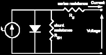
14 Resistive effects Characteristic resistance Parasitic resistance Resistive effects Characteristic resistance Maximum power transfer is R LOAD = R CH Resistive effects Characteristic resistance Parasitic resistance Series resistance Shunt resistance 14
15 Resistive effects Characteristic resistance Parasitic resistance Series resistance Shunt resistance Effect of the series resistance with I sc Medium Rs Large Rs V oc Slope of the I-V curve near V oc gives indication about R s Effect of the shunt resistance with I sc Medium R sh Large R sh V oc Slope of the I-V curve near Isc gives indication about Rsh 15


16 Effect of irradiation Current Voltage Effect of temperature Current Temperature increase reduces voltage by 2.2 mv/ o C Voltage 16


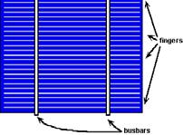
17 Optical losses - light which could have generated an electron-hole pair, but does not, because the light is reflected from the front surface, or because it is not absorbed in the solar cell. Optical losses - light which could have generated an electron-hole pair, but does not, because the light is reflected from the front surface, or because it is not absorbed in the solar cell. Top contact shading Top surface reflection Not enought optical path for photon absorption Optical losses Reduce shading from top contacts 17


")
 ARC (")
 18")
18 Optical losses Reduce shading from top contacts Optical losses Reduce shading from top contacts May increase series resistance Other emitter contact concepts becoming fashionable (burried or back contacts) Optical losses Anti-reflective coating n1 d 4 Air ( n 0 ) ARC ( n 1 ) 2 n1 n0 n 2 R 2 n1 n0 n2 2 Silicon ( n 2 ) 18


19 Optical losses Anti-reflective coating Optical losses Surface texturing Optical losses Surface texturing Single crystal: Random pyramids, by etching Multi crystal: texturing by photolithography Single crystal: Inverted pyramids, by etching Multi crystal: texturing by macroporous silicon 19


20 Optical losses Light trapping: increase optical length Optical losses Light trapping: increase optical length Optical losses Light trapping: increase optical length Snell s law of refraction: 20


21 Optical losses Light trapping: increase optical length Snell s law of refraction: Optical losses In summary: Reduce front contact coverage Anti-reflective coating Surface texturing Light trapping Recombination losses Optimal conditions: the carrier must be generated within a diffusion length of the junction; the carrier must be generated closer to the junction than to hazardous recombination sites (unpassivated surface, grain boundary, ) 21

 Design of silicon solar cells Recombination losses: Surface passivation 22")
22 Recombination losses Design of silicon solar cells Recombination losses: Surface passivation Reducing the number of dangling bonds by growing a SiO 2 or SiN thin film on the surface (also for anti-reflection coating; notice that it is an electric insulator) Increasing doping, creating a repelling field (decreases diffusion length thus not suitable for charge collection region; useful closer to contacts, e.g. Back Surface Field - BSF) Design of silicon solar cells Recombination losses: Surface passivation 22

 Prog. Photovolt: Res. Appl.")
23 Single junction silicon solar cell Best lab cell: 25% J. Zhao et al Novel 19.8% efficient honeycomb textured multicrystalline and 24.4% monocrystalline silicon solar cells. Applied Physics Letters 1998; 73: Best module: 23% M. Green et al, Solar Cell Efficiency Tables (Version 34) Prog. Photovolt: Res. Appl. 2009; 17: Practical cell design (for industry!) requires compromises, and thus lower efficiencies Check February issue of Photon International 23


")
24 Practical cell design (for industry!) requires compromises, and thus lower efficiencies Next class How to make a practical photovoltaic module Other (non-silicon) technologies And a new set of exercises 24
What is the highest efficiency Solar Cell?
 What is the highest efficiency Solar Cell? GT CRC Roof-Mounted PV System Largest single PV structure at the time of it s construction for the 1996 Olympic games Produced more than 1 billion watt hrs. of
Solar Cell Parameters and Equivalent Circuit
 9 Solar Cell Parameters and Equivalent Circuit 9.1 External solar cell parameters The main parameters that are used to characterise the performance of solar cells are the peak power P max, the short-circuit
EE Solar Cell Opreation. Y. Baghzouz Professor of Electrical Engineering
 EE 495-695 4.2 Solar Cell Opreation Y. Baghzouz Professor of Electrical Engineering Characteristic Resistance The characteristic resistance of a solar cell is the output resistance of the solar cell at
LEDs, Photodetectors and Solar Cells
 LEDs, Photodetectors and Solar Cells Chapter 7 (Parker) ELEC 424 John Peeples Why the Interest in Photons? Answer: Momentum and Radiation High electrical current density destroys minute polysilicon and
Introduction to Photovoltaics
 Introduction to Photovoltaics PHYS 4400, Principles and Varieties of Solar Energy Instructor: Randy J. Ellingson The University of Toledo February 24, 2015 Only solar energy Of all the possible sources
Performance and Loss Analyses of High-Efficiency CBD-ZnS/Cu(In 1-x Ga x )Se 2 Thin-Film Solar Cells
Se 2 Thin-Film Solar Cells") Performance and Loss Analyses of High-Efficiency CBD-ZnS/Cu(In 1-x Ga x )Se 2 Thin-Film Solar Cells Alexei Pudov 1, James Sites 1, Tokio Nakada 2 1 Department of Physics, Colorado State University, Fort
Performance and Loss Analyses of High-Efficiency CBD-ZnS/Cu(In 1-x Ga x )Se 2 Thin-Film Solar Cells Alexei Pudov 1, James Sites 1, Tokio Nakada 2 1 Department of Physics, Colorado State University, Fort
CHAPTER-2 Photo Voltaic System - An Overview
 CHAPTER-2 Photo Voltaic System - An Overview 15 CHAPTER-2 PHOTO VOLTAIC SYSTEM -AN OVERVIEW 2.1 Introduction With the depletion of traditional energies and the increase in pollution and greenhouse gases
Problem 4 Consider a GaAs p-n + junction LED with the following parameters at 300 K: Electron diusion coecient, D n = 25 cm 2 =s Hole diusion coecient
 Prof. Jasprit Singh Fall 2001 EECS 320 Homework 7 This homework is due on November 8. Problem 1 An optical power density of 1W/cm 2 is incident on a GaAs sample. The photon energy is 2.0 ev and there is
Key Questions ECE 340 Lecture 28 : Photodiodes
 Things you should know when you leave Key Questions ECE 340 Lecture 28 : Photodiodes Class Outline: How do the I-V characteristics change with illumination? How do solar cells operate? How do photodiodes
Quality Assurance in Solar with the use of I-V Curves
 Quality Assurance in Solar with the use of I-V Curves Eternal Sun Whitepaper Written by: RJ van Vugt Introduction I Installers, wholesalers and other parties use performance tests in order to check on
SILICON NANOWIRE HYBRID PHOTOVOLTAICS
 SILICON NANOWIRE HYBRID PHOTOVOLTAICS Erik C. Garnett, Craig Peters, Mark Brongersma, Yi Cui and Mike McGehee Stanford Univeristy, Department of Materials Science, Stanford, CA, USA ABSTRACT Silicon nanowire
Fall 2004 Dawn Hettelsater, Yan Zhang and Ali Shakouri, 05/09/2002
 University of California at Santa Cruz Jack Baskin School of Engineering Electrical Engineering Department EE-145L: Properties of Materials Laboratory Lab 6: Solar Cells Fall 2004 Dawn Hettelsater, Yan
Lecture 18: Photodetectors
 Lecture 18: Photodetectors Contents 1 Introduction 1 2 Photodetector principle 2 3 Photoconductor 4 4 Photodiodes 6 4.1 Heterojunction photodiode.................... 8 4.2 Metal-semiconductor photodiode................
2nd Asian Physics Olympiad
 2nd Asian Physics Olympiad TAIPEI, TAIWAN Experimental Competition Thursday, April 26, 21 Time Available : 5 hours Read This First: 1. Use only the pen provided. 2. Use only the front side of the answer
ANISOTYPE GaAs BASED HETEROJUNCTIONS FOR III-V MULTIJUNCTION SOLAR CELLS
 ANISOTYPE Ga BASED HETEROJUNCTIONS FOR III-V MULTIJUNCTION SOLAR CELLS A.S. Gudovskikh 1,*, K.S. Zelentsov 1, N.A. Kalyuzhnyy 2, V.M. Lantratov 2, S.A. Mintairov 2 1 Saint-Petersburg Academic University
Modelling and Analysis of Four-Junction Tendem Solar Cell in Different Environmental Conditions Mr. Biraju J. Trivedi 1 Prof. Surendra Kumar Sriwas 2
 IJSRD - International Journal for Scientific Research & Development Vol. 3, Issue 08, 2015 ISSN (online): 2321-0613 Modelling and Analysis of Four-Junction Tendem Solar Cell in Different Environmental
Review of Semiconductor Physics
 Review of Semiconductor Physics k B 1.38 u 10 23 JK -1 a) Energy level diagrams showing the excitation of an electron from the valence band to the conduction band. The resultant free electron can freely
PHYSICAL ELECTRONICS(ECE3540) APPLICATIONS OF PHYSICAL ELECTRONICS PART I
 APPLICATIONS OF PHYSICAL ELECTRONICS PART I") PHYSICAL ELECTRONICS(ECE3540) APPLICATIONS OF PHYSICAL ELECTRONICS PART I Tennessee Technological University Monday, October 28, 2013 1 Introduction In the following slides, we will discuss the summary
PHYSICAL ELECTRONICS(ECE3540) APPLICATIONS OF PHYSICAL ELECTRONICS PART I Tennessee Technological University Monday, October 28, 2013 1 Introduction In the following slides, we will discuss the summary
10/27/2009 Reading: Chapter 10 of Hambley Basic Device Physics Handout (optional)
") EE40 Lec 17 PN Junctions Prof. Nathan Cheung 10/27/2009 Reading: Chapter 10 of Hambley Basic Device Physics Handout (optional) Slide 1 PN Junctions Semiconductor Physics of pn junctions (for reference
EE40 Lec 17 PN Junctions Prof. Nathan Cheung 10/27/2009 Reading: Chapter 10 of Hambley Basic Device Physics Handout (optional) Slide 1 PN Junctions Semiconductor Physics of pn junctions (for reference
Simulation of silicon based thin-film solar cells. Copyright Crosslight Software Inc.
 Simulation of silicon based thin-film solar cells Copyright 1995-2008 Crosslight Software Inc. www.crosslight.com 1 Contents 2 Introduction Physical models & quantum tunneling Material properties Modeling
Chapter 4. Impact of Dust on Solar PV Module: Experimental Analysis
 Chapter 4 Impact of Dust on Solar PV Module: Experimental Analysis 53 CHAPTER 4 IMPACT OF DUST ON SOLAR PV MODULE: EXPERIMENTAL ANALYSIS 4.1 INTRODUCTION: On a bright, sunny day the sun shines approximately
ECE 340 Lecture 29 : LEDs and Lasers Class Outline:
 ECE 340 Lecture 29 : LEDs and Lasers Class Outline: Light Emitting Diodes Lasers Semiconductor Lasers Things you should know when you leave Key Questions What is an LED and how does it work? How does a
Key Questions. What is an LED and how does it work? How does a laser work? How does a semiconductor laser work? ECE 340 Lecture 29 : LEDs and Lasers
 Things you should know when you leave Key Questions ECE 340 Lecture 29 : LEDs and Class Outline: What is an LED and how does it How does a laser How does a semiconductor laser How do light emitting diodes
OPTOELECTRONIC and PHOTOVOLTAIC DEVICES
 OPTOELECTRONIC and PHOTOVOLTAIC DEVICES Outline 1. Introduction to the (semiconductor) physics: energy bands, charge carriers, semiconductors, p-n junction, materials, etc. 2. Light emitting diodes Light
Thin film PV Technologies III- V PV Technology
 Thin film PV Technologies III- V PV Technology Week 5.1 Arno Smets ` (Source: NASA) III V PV Technology Semiconductor Materials III- V semiconductors: GaAs: GaP: InP: InAs: GaInAs: GaInP: AlGaInAs: AlGaInP:
A Thesis submitted in partial fulfillment of the requirements for the degree of Master of Science at George Mason University
 Auger Suppression in MWIR InSb Photodiode for Ambient Temperature Operation A Thesis submitted in partial fulfillment of the requirements for the degree of Master of Science at George Mason University
1 Semiconductor-Photon Interaction
 1 SEMICONDUCTOR-PHOTON INTERACTION 1 1 Semiconductor-Photon Interaction Absorption: photo-detectors, solar cells, radiation sensors. Radiative transitions: light emitting diodes, displays. Stimulated emission:
Solar Cell I-V Characteristics
 Chapter 3 Solar Cell I-V Characteristics It is well known that the behaviour of a PhotoVoltaic PV) System is greatly influenced by factors such as the solar irradiance availability and distribution and
Modelling and simulation of PV module for different irradiation levels Balachander. K Department of EEE, Karpagam University, Coimbatore.
 6798 Available online at www.elixirpublishers.com (Elixir International Journal) Electrical Engineering Elixir Elec. Engg. 43 (2012) 6798-6802 Modelling and simulation of PV module for different irradiation
Lecture 7:PN Junction. Structure, Depletion region, Different bias Conditions, IV characteristics, Examples
 Lecture 7:PN Junction Structure, Depletion region, Different bias Conditions, IV characteristics, Examples PN Junction The diode (pn junction) is formed by dopping a piece of intrinsic silicon, such that
CHAPTER 3 PHOTOVOLTAIC SYSTEM MODEL WITH CHARGE CONTROLLERS
 34 CHAPTER 3 PHOTOVOLTAIC SYSTEM MODEL WITH CHARGE CONTROLLERS Solar photovoltaics are used for the direct conversion of solar energy into electrical energy by means of the photovoltaic effect, that is,
INCREASED CELL EFFICIENCY IN InGaAs THIN FILM SOLAR CELLS WITH DIELECTRIC AND METAL BACK REFLECTORS
 INCREASED CELL EFFICIENCY IN InGaAs THIN FILM SOLAR CELLS WITH DIELECTRIC AND METAL BACK REFLECTORS Koray Aydin, Marina S. Leite and Harry A. Atwater Thomas J. Watson Laboratories of Applied Physics, California
Design and Performance of InGaAs/GaAs Based Tandem Solar Cells
 American Journal of Engineering Research (AJER) e-issn: 2320-0847 p-issn : 2320-0936 Volume-5, Issue-11, pp-64-69 www.ajer.org Research Paper Open Access Design and Performance of InGaAs/GaAs Based Tandem
Light management in photovoltaics using nanotechnology
 Light management in photovoltaics using nanotechnology Albert Polman Center for Nanophotonics FOM-Institute AMOLF Amsterdam, The Netherlands Solar irradiance on earth assuming 30% PV, 175 W/m 2 Solar
Solar Cells, Modules, Arrays, and Characterization
 ... energizing Ohio for the 21st Century Solar Cells, Modules, Arrays, and Characterization April 17, 2014 The University of Toledo, Department of Physics and Astronomy SSARE, PVIC Principles and Varieties
Luminous Equivalent of Radiation
 Intensity vs λ Luminous Equivalent of Radiation When the spectral power (p(λ) for GaP-ZnO diode has a peak at 0.69µm) is combined with the eye-sensitivity curve a peak response at 0.65µm is obtained with
Fundamentals of CMOS Image Sensors
 CHAPTER 2 Fundamentals of CMOS Image Sensors Mixed-Signal IC Design for Image Sensor 2-1 Outline Photoelectric Effect Photodetectors CMOS Image Sensor(CIS) Array Architecture CIS Peripherals Design Considerations
Electronic devices-i. Difference between conductors, insulators and semiconductors
 Electronic devices-i Semiconductor Devices is one of the important and easy units in class XII CBSE Physics syllabus. It is easy to understand and learn. Generally the questions asked are simple. The unit
Laser Edge Isolation for High-efficiency Crystalline Silicon Solar Cells
 Journal of the Korean Physical Society, Vol. 55, No. 1, July 2009, pp. 124 128 Laser Edge Isolation for High-efficiency Crystalline Silicon Solar Cells Dohyeon Kyeong, Muniappan Gunasekaran, Kyunghae Kim,
Unit 2 Semiconductor Devices. Lecture_2.5 Opto-Electronic Devices
 Unit 2 Semiconductor Devices Lecture_2.5 Opto-Electronic Devices Opto-electronics Opto-electronics is the study and application of electronic devices that interact with light. Electronics (electrons) Optics
14.2 Photodiodes 411
 14.2 Photodiodes 411 Maximum reverse voltage is specified for Ge and Si photodiodes and photoconductive cells. Exceeding this voltage can cause the breakdown and severe deterioration of the sensor s performance.
Optical Amplifiers. Continued. Photonic Network By Dr. M H Zaidi
 Optical Amplifiers Continued EDFA Multi Stage Designs 1st Active Stage Co-pumped 2nd Active Stage Counter-pumped Input Signal Er 3+ Doped Fiber Er 3+ Doped Fiber Output Signal Optical Isolator Optical
Available online at ScienceDirect. Energy Procedia 92 (2016 ) 10 15
 10 15") Available online at www.sciencedirect.com ScienceDirect Energy Procedia 92 (16 ) 15 6th International Conference on Silicon Photovoltaics, SiliconPV 16 Local solar cell efficiency analysis performed by
Available online at www.sciencedirect.com ScienceDirect Energy Procedia 92 (16 ) 15 6th International Conference on Silicon Photovoltaics, SiliconPV 16 Local solar cell efficiency analysis performed by
Optical Receivers Theory and Operation
 Optical Receivers Theory and Operation Photo Detectors Optical receivers convert optical signal (light) to electrical signal (current/voltage) Hence referred O/E Converter Photodetector is the fundamental
Optimising Layer Thickness of Multi-Junction Silicon Devices for Energy Production in a Maritime Climate
 Optimising Layer Thickness of Multi-Junction Silicon Devices for Energy Production in a Maritime Climate S. Andre, T.R. Betts, R. Gottschalg *, D.G. Infield Centre for Renewable Energy Systems Technology,
Silicon sensors for radiant signals. D.Sc. Mikko A. Juntunen
 Silicon sensors for radiant signals D.Sc. Mikko A. Juntunen 2017 01 16 Today s outline Introduction Basic physical principles PN junction revisited Applications Light Ionizing radiation X-Ray sensors in
CONTENTS. 2.2 Schrodinger's Wave Equation 31. PART I Semiconductor Material Properties. 2.3 Applications of Schrodinger's Wave Equation 34
 CONTENTS Preface x Prologue Semiconductors and the Integrated Circuit xvii PART I Semiconductor Material Properties CHAPTER 1 The Crystal Structure of Solids 1 1.0 Preview 1 1.1 Semiconductor Materials
Light Sources, Modulation, Transmitters and Receivers
 Optical Fibres and Telecommunications Light Sources, Modulation, Transmitters and Receivers Introduction Previous section looked at Fibres. How is light generated in the first place? How is light modulated?
Department of Electrical Engineering IIT Madras
 Department of Electrical Engineering IIT Madras Sample Questions on Semiconductor Devices EE3 applicants who are interested to pursue their research in microelectronics devices area (fabrication and/or
Electrical Characterization
 Listing and specification of characterization equipment at ISC Konstanz 30.05.2016 Electrical Characterization µw-pcd (Semilab) PV2000 (Semilab) - spatially resolved minority charge carrier lifetime -diffusion
Reference: Photovoltaic Systems, p
 PV systems are comprised of building blocks of cells, modules and arrays to form a DC power generating unit with specified electrical output. Reference: Photovoltaic Systems, p. 115-118 Reference: Photovoltaic
OFCS OPTICAL DETECTORS 11/9/2014 LECTURES 1
 OFCS OPTICAL DETECTORS 11/9/2014 LECTURES 1 1-Defintion & Mechanisms of photodetection It is a device that converts the incident light into electrical current External photoelectric effect: Electrons are
Semiconductor Lasers Semiconductors were originally pumped by lasers or e-beams First diode types developed in 1962: Create a pn junction in
 Semiconductor Lasers Semiconductors were originally pumped by lasers or e-beams First diode types developed in 1962: Create a pn junction in semiconductor material Pumped now with high current density
CCD Analogy BUCKETS (PIXELS) HORIZONTAL CONVEYOR BELT (SERIAL REGISTER) VERTICAL CONVEYOR BELTS (CCD COLUMNS) RAIN (PHOTONS)
 HORIZONTAL CONVEYOR BELT (SERIAL REGISTER) VERTICAL CONVEYOR BELTS (CCD COLUMNS) RAIN (PHOTONS)") CCD Analogy RAIN (PHOTONS) VERTICAL CONVEYOR BELTS (CCD COLUMNS) BUCKETS (PIXELS) HORIZONTAL CONVEYOR BELT (SERIAL REGISTER) MEASURING CYLINDER (OUTPUT AMPLIFIER) Exposure finished, buckets now contain
CCD Analogy RAIN (PHOTONS) VERTICAL CONVEYOR BELTS (CCD COLUMNS) BUCKETS (PIXELS) HORIZONTAL CONVEYOR BELT (SERIAL REGISTER) MEASURING CYLINDER (OUTPUT AMPLIFIER) Exposure finished, buckets now contain
Quantum Efficiency Measurement System with Internal Quantum Efficiency Upgrade
 Quantum Efficiency Measurement System with Internal Quantum Efficiency Upgrade QE / IPCE SYSTEM Upgraded with Advanced Features Includes IV Testing, Spectral Response, Quantum Efficiency System/ IPCE System
CHAPTER 5 CIRCUIT MODELING METHODOLOGY FOR THIN-FILM PHOTOVOLTAIC MODULES
 106 CHAPTER 5 CIRCUIT MODELING METHODOLOGY FOR THIN-FILM PHOTOVOLTAIC MODULES 5.1 INTRODUCTION In this Chapter, the constructional details of various thin-film modules required for modeling are given.
Photodiode: LECTURE-5
 LECTURE-5 Photodiode: Photodiode consists of an intrinsic semiconductor sandwiched between two heavily doped p-type and n-type semiconductors as shown in Fig. 3.2.2. Sufficient reverse voltage is applied
EQE Measurements in Mid-Infrared Superlattice Structures
 University of Iowa Honors Theses University of Iowa Honors Program Spring 2018 EQE Measurements in Mid-Infrared Superlattice Structures Andrew Muellerleile Follow this and additional works at: http://ir.uiowa.edu/honors_theses
ANALYSIS OF MATHEMATICAL MODEL OF PV MODULE USING MATLAB/SIMULINK ENVIRONMENT: REVIEW
 ANALYSIS OF MATHEMATICAL MODEL OF PV MODULE USING MATLAB/SIMULINK ENVIRONMENT: REVIEW 1 NISHA PATEL, 2 Hardik Patel, 3 Ketan Bariya 1 M.E. Student, 2 Assistant Professor, 3 Assistant Professor 1 Electrical
I D = I so e I. where: = constant T = junction temperature [K] I so = inverse saturating current I = photovoltaic current
![I D = I so e I. where: = constant T = junction temperature [K] I so = inverse saturating current I = photovoltaic current](/thumbs/83/87981810.jpg "I D = I so e I. where: = constant T = junction temperature [K] I so = inverse saturating current I = photovoltaic current") H7. Photovoltaics: Solar Power I. INTRODUCTION The sun is practically an endless source of energy. Most of the energy used in the history of mankind originated from the sun (coal, petroleum, etc.). The
H7. Photovoltaics: Solar Power I. INTRODUCTION The sun is practically an endless source of energy. Most of the energy used in the history of mankind originated from the sun (coal, petroleum, etc.). The
FLATE Hillsborough Community College - Brandon (813)
") The Florida Advanced Technological Education (FLATE) Center wishes to make available, for educational and noncommercial purposes only, materials relevant to the EST1830 Introduction to Alternative/Renewable
The Florida Advanced Technological Education (FLATE) Center wishes to make available, for educational and noncommercial purposes only, materials relevant to the EST1830 Introduction to Alternative/Renewable
LIGHT SENSING PERFORMANCE OF AMORPHOUS SILICON THIN FILM PIN DIODES: STRUCTURE, INCIDENT LIGHT, AND PLASMA DEPOSITION EFFECTS.
 LIGHT SENSING PERFORMANCE OF AMORPHOUS SILICON THIN FILM PIN DIODES: STRUCTURE, INCIDENT LIGHT, AND PLASMA DEPOSITION EFFECTS A Thesis by KAI PATRICK HENRY Submitted to the Office of Graduate and Professional
Recent Development and Study of Silicon Solid State Photomultiplier (MRS Avalanche Photodetector)
") Recent Development and Study of Silicon Solid State Photomultiplier (MRS Avalanche Photodetector) Valeri Saveliev University of Obninsk, Russia Vienna Conference on Instrumentation Vienna, 20 February
Recent Development and Study of Silicon Solid State Photomultiplier (MRS Avalanche Photodetector) Valeri Saveliev University of Obninsk, Russia Vienna Conference on Instrumentation Vienna, 20 February
Volume 11 - Number 19 - May 2015 (66-71) Practical Identification of Photovoltaic Module Parameters
 Practical Identification of Photovoltaic Module Parameters") ISESCO JOURNAL of Science and Technology Volume 11 - Number 19 - May 2015 (66-71) Abstract The amount of energy radiated to the earth by the sun exceeds the annual energy requirement of the world population.
ISESCO JOURNAL of Science and Technology Volume 11 - Number 19 - May 2015 (66-71) Abstract The amount of energy radiated to the earth by the sun exceeds the annual energy requirement of the world population.
UNIT III. By Ajay Kumar Gautam Asst. Prof. Electronics & Communication Engineering Dev Bhoomi Institute of Technology & Engineering, Dehradun
 UNIT III By Ajay Kumar Gautam Asst. Prof. Electronics & Communication Engineering Dev Bhoomi Institute of Technology & Engineering, Dehradun SYLLABUS Optical Absorption in semiconductors, Types of Photo
An Evaluation of Constituents in Paste for Silicon Solar Cells with Floating Contact Method: A Case Study of Tellurium Oxide
 7 th Metallization Workshop, Konstanz, Germany, 2017 An Evaluation of Constituents in Paste for Silicon Solar Cells with Floating Contact Method: A Case Study of Tellurium Oxide Takayuki Aoyama 1, 2, Mari
Electronics The basics of semiconductor physics
 Electronics The basics of semiconductor physics Prof. Márta Rencz, Gábor Takács BME DED 17/09/2015 1 / 37 The basic properties of semiconductors Range of conductivity [Source: http://www.britannica.com]
Digital Integrated Circuits A Design Perspective. The Devices. Digital Integrated Circuits 2nd Devices
 Digital Integrated Circuits A Design Perspective The Devices The Diode The diodes are rarely explicitly used in modern integrated circuits However, a MOS transistor contains at least two reverse biased
Comparison Of GaAs (III-Vsemiconductors) And Si Vertical Multijunction Solar Cells, As The Converters In The Power Beaming Systems
 And Si Vertical Multijunction Solar Cells, As The Converters In The Power Beaming Systems") IOSR Journal of Electrical and Electronics Engineering (IOSR-JEEE) e-issn: 2278-1676,p-ISSN: 2320-3331, Volume 11, Issue 4 Ver. I (Jul. Aug. 2016), PP 145-150 www.iosrjournals.org Comparison Of GaAs (III-Vsemiconductors)
IOSR Journal of Electrical and Electronics Engineering (IOSR-JEEE) e-issn: 2278-1676,p-ISSN: 2320-3331, Volume 11, Issue 4 Ver. I (Jul. Aug. 2016), PP 145-150 www.iosrjournals.org Comparison Of GaAs (III-Vsemiconductors)
Thin Film Group II-VI Solar Cells Based on Band-Offsets
 Portland State University PDXScholar Dissertations and Theses Dissertations and Theses 1-1-2010 Thin Film Group II-VI Solar Cells Based on Band-Offsets James Keith Walton Portland State University Let
Semiconductor Lasers Semiconductors were originally pumped by lasers or e-beams First diode types developed in 1962: Create a pn junction in
 Semiconductor Lasers Semiconductors were originally pumped by lasers or e-beams First diode types developed in 1962: Create a pn junction in semiconductor material Pumped now with high current density
LED lecture. Wei Chih Wang University of Washington
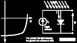
 LED lecture Wei Chih Wang University of Washington Linear and Nonlinear electronics current voltage Vaccum tube (i.e. type 2A3) voltage Thermistor (large negative temperature coefficient of resistivity)
Semiconductor Physics and Devices
 Metal-Semiconductor and Semiconductor Heterojunctions The Metal-Oxide-Semiconductor Field-Effect Transistor (MOSFET) is one of two major types of transistors. The MOSFET is used in digital circuit, because
Solar-energy conversion and light emission in an atomic monolayer p n diode
 Solar-energy conversion and light emission in an atomic monolayer p n diode Andreas Pospischil, Marco M. Furchi, and Thomas Mueller 1. I-V characteristic of WSe 2 p-n junction diode in the dark The Shockley
Physics and Technology
 Physics and Technology Emitters Materials Infrared emitting diodes (IREDs) can be produced from a range of different III-V compounds. Unlike the elemental semiconductor silicon, the compound III-V semiconductors
The Role of Mirror Dichroic in Tandem Solar Cell GaAs/Si
 The Role of Mirror Dichroic in Tandem Solar Cell GaAs/Si Hemmani Abderrahmane * Dennai Benmoussa H Benslimane A Helmaoui hysics laboratory in semiconductor devices, Department of hysics, University of
Basic concepts. Optical Sources (b) Optical Sources (a) Requirements for light sources (b) Requirements for light sources (a)
 Optical Sources (a) Requirements for light sources (b) Requirements for light sources (a)") Optical Sources (a) Optical Sources (b) The main light sources used with fibre optic systems are: Light-emitting diodes (LEDs) Semiconductor lasers (diode lasers) Fibre laser and other compact solid-state
Optical Sources (a) Optical Sources (b) The main light sources used with fibre optic systems are: Light-emitting diodes (LEDs) Semiconductor lasers (diode lasers) Fibre laser and other compact solid-state
Università degli Studi di Roma Tor Vergata Dipartimento di Ingegneria Elettronica. Analogue Electronics. Paolo Colantonio A.A.
 Università degli Studi di Roma Tor Vergata Dipartimento di Ingegneria Elettronica Analogue Electronics Paolo Colantonio A.A. 2015-16 Introduction: materials Conductors e.g. copper or aluminum have a cloud
Optical Fiber Communication Lecture 11 Detectors
 Optical Fiber Communication Lecture 11 Detectors Warriors of the Net Detector Technologies MSM (Metal Semiconductor Metal) PIN Layer Structure Semiinsulating GaAs Contact InGaAsP p 5x10 18 Absorption InGaAs
CHAPTER 8 The PN Junction Diode
 CHAPTER 8 The PN Junction Diode Consider the process by which the potential barrier of a PN junction is lowered when a forward bias voltage is applied, so holes and electrons can flow across the junction
Quantum Condensed Matter Physics Lecture 16
 Quantum Condensed Matter Physics Lecture 16 David Ritchie QCMP Lent/Easter 2018 http://www.sp.phy.cam.ac.uk/drp2/home 16.1 Quantum Condensed Matter Physics 1. Classical and Semi-classical models for electrons
Chapter 3: Basics Semiconductor Devices and Processing 2006/9/27 1. Topics
 Chapter 3: Basics Semiconductor Devices and Processing 2006/9/27 1 Topics What is semiconductor Basic semiconductor devices Basics of IC processing CMOS technologies 2006/9/27 2 1 What is Semiconductor
value of W max for the device. The at band voltage is -0.9 V. Problem 5: An Al-gate n-channel MOS capacitor has a doping of N a = cm ;3. The oxi
 Prof. Jasprit Singh Fall 2001 EECS 320 Homework 10 This homework is due on December 6 Problem 1: An n-type In 0:53 Ga 0:47 As epitaxial layer doped at 10 16 cm ;3 is to be used as a channel in a FET. A
LAB V. LIGHT EMITTING DIODES
 LAB V. LIGHT EMITTING DIODES 1. OBJECTIVE In this lab you are to measure I-V characteristics of Infrared (IR), Red and Blue light emitting diodes (LEDs). The emission intensity as a function of the diode
Chapter 4 OPTICAL DETECTORS
 Chapter 4 OPTICAL DETECTORS (Reference: Optical Electronics in Modern Communications, A. Yariv, Oxford, 1977, Ch. 11.) Photomultiplier Tube (PMT) Highly sensitive detector for light from near infrared
Photovoltaic Cells for Optical Power and Data Transmission
 Photovoltaic Cells for Optical Power and Transmission H. Helmers, S.P. Philipps, S.K. Reichmuth, E. Oliva, D. Lackner, A.W. Bett Fraunhofer Institute for Solar Energy Systems ISE European Telemetry and
Physics of Waveguide Photodetectors with Integrated Amplification
 Physics of Waveguide Photodetectors with Integrated Amplification J. Piprek, D. Lasaosa, D. Pasquariello, and J. E. Bowers Electrical and Computer Engineering Department University of California, Santa
Part I. CCD Image Sensors
 Part I CCD Image Sensors 2 Overview of CCD CCD is the abbreviation for charge-coupled device. CCD image sensors are silicon-based integrated circuits (ICs), consisting of a dense matrix of photodiodes
Design and Simulation of N-Substrate Reverse Type Ingaasp/Inp Avalanche Photodiode
 International Refereed Journal of Engineering and Science (IRJES) ISSN (Online) 2319-183X, (Print) 2319-1821 Volume 2, Issue 8 (August 2013), PP.34-39 Design and Simulation of N-Substrate Reverse Type
Tradeoffs of the use of SiGe buffer layers in tandem GaAsP/Si solar cells
 Tradeoffs of the use of SiGe buffer layers in tandem GaAsP/Si solar cells by Evelina Aleksandrova Polyzoeva B.Sc., Electronics, Technical University of Sofia (2004) M.Sc., Electronics, Technical University
Response of GaAs Photovoltaic Converters Under Pulsed Laser Illumination
 Response of GaAs Photovoltaic Converters Under Pulsed Laser Illumination TIQIANG SHAN 1, XINGLIN QI 2 The Third Department Mechanical Engineering College Shijiazhuang, Hebei CHINA stq0701@163.com 1, xinling399@163.com
ELECTRONIC DEVICES AND CIRCUITS
 ELECTRONIC DEVICES AND CIRCUITS 1. At room temperature the current in an intrinsic semiconductor is due to A. holes B. electrons C. ions D. holes and electrons 2. Work function is the maximum energy required
Modeling of Electrical Characteristics of Photovoltaic Cell Considering Single-Diode Model
 Journal of Clean Energy Technologies, Vol. 4, No. 6, November 2016 Modeling of Electrical Characteristics of Photovoltaic Cell Considering Single-Diode Model M. Azzouzi, D. Popescu, and M. Bouchahdane
Laboratory 2: PV Module Current-Voltage Measurements
 Laboratory 2: PV Module Current-Voltage Measurements Introduction and Background The current-voltage (I-V) characteristic is the basic descriptor of photovoltaic device performance. A fundamental understanding
EXPERIMENTAL STUDY OF METEOROLOGICAL EFFECTS ON SOLAR SPECTRUM APPLIED TO PREDICT DIFFERENT PHOTOVOLTAIC TECHNOLOGIES
 EXPERIMENTAL STUDY OF METEOROLOGICAL EFFECTS ON SOLAR SPECTRUM APPLIED TO PREDICT DIFFERENT PHOTOVOLTAIC TECHNOLOGIES A THESIS SUBMITTED TO THE GRADUATE DIVISION OF THE UNIVERSITY OF HAWAI I AT MĀNOA IN
Physics 160 Lecture 5. R. Johnson April 13, 2015
 Physics 160 Lecture 5 R. Johnson April 13, 2015 Half Wave Diode Rectifiers Full Wave April 13, 2015 Physics 160 2 Note that there is no ground connection on this side of the rectifier! Output Smoothing
Photonic Crystal Slot Waveguide Spectrometer for Detection of Methane
 Photonic Crystal Slot Waveguide Spectrometer for Detection of Methane Swapnajit Chakravarty 1, Wei-Cheng Lai 2, Xiaolong (Alan) Wang 1, Che-Yun Lin 2, Ray T. Chen 1,2 1 Omega Optics, 10306 Sausalito Drive,
Lecture 6 Fiber Optical Communication Lecture 6, Slide 1
 Lecture 6 Optical transmitters Photon processes in light matter interaction Lasers Lasing conditions The rate equations CW operation Modulation response Noise Light emitting diodes (LED) Power Modulation
Dr E. Kaplani. Mechanical Engineering Dept. T.E.I. of Patras, Greece
 Innovation Week on PV Systems Engineering and the other Renewable Energy Systems. 1-10 July 2013, Patras, Greece Dr E. Kaplani ekaplani@teipat.gr Mechanical Engineering Dept. T.E.I. of Patras, Greece R.E.S.
Investigation of Photovoltaic Properties of In:ZnO/SiO 2 /p- Si Thin Film Devices
 Universities Research Journal 2011, Vol. 4, No. 4 Investigation of Photovoltaic Properties of In:ZnO/SiO 2 /p- Si Thin Film Devices Kay Thi Soe 1, Moht Moht Than 2 and Win Win Thar 3 Abstract This study