Light management in photovoltaics using nanotechnology
|
|
|
- Jeffery Benson
- 5 years ago
- Views:
Transcription
1 Light management in photovoltaics using nanotechnology Albert Polman Center for Nanophotonics FOM-Institute AMOLF Amsterdam, The Netherlands

2
3 Solar irradiance on earth assuming 30% PV, 175 W/m 2
4 Solar irradiance on earth assuming 30% PV, 175 W/m 2

5 Solar irradiance on earth assuming 30% PV, 175 W/m 2
6 The solar spectrum T sun =5800 K Si bandgap
7 The solar spectrum polymer bandgap T sun =5800 K
 image: ESO/M.")
8 Proxima centauri Discovered in 2016 Nature 536, 437 (2016) image: ESO/M. Kornmesser
9 Proxima centauri spectrum Spectral intensity (W/m 2 /nm) T PC =3042 K Si bandgap Si solar cell 25 14% Wa v e le(nm) n g t h
10 Proxima centauri spectrum Spectral intensity (W/m 2 /nm) polymer bandgap polymer solar cell 11 3% T PC =3042 K Wa v e le(nm) n g t h


11 Our solar spectrum - visible spectrum T sun =5800 K
12 Solar cell basic design

13 The solar spectrum T sun =5800 K
14 Absorption edge and quantum defect Quantum defect E g Absorption above bandgap
15 Voltage is lower than bandgap energy I ext = I 0 exp(v/kt)-i SC
16 Voltage is lower than bandgap energy I ext = I 0 exp(v/kt)-i SC
17 Voltage is lower than bandgap energy I ext = I 0 exp(v/kt)-i SC
18 Voltage is lower than bandgap energy E g
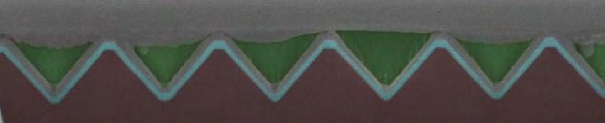
19 Voltage is lower than bandgap energy E g 34 %


20 Shockley-Queisser efficiency limit: 34% 34% W. Shockley, H. J. Queisser Detailed balance limit of efficiency of p-n junction solar cells J. Appl. Phys 32, (1961)

21 Record solar cell efficiencies Science 352, 207 (2016)
22 J sc and V oc relative to SQ limit for each material carrier management AMOLF light management Science 352, 207 (2016)


23 J sc and V oc relative to SQ limit for each material carrier management AMOLF light management Schrődinger Maxwell Science 352, 207 (2016)


24 The light scattering solar cell Light coupling and trapping by resonant light scatterers 4% n=1.0 n=3.5 96% H.A. Atwater and A. Polman Nature Mater. 9, 205 (2010), Nature Mater. 11, 174 (2012)
25 Plasmonic vs. dielectric particles Q = scat C C scat geom Metal nanoparticle: plasmonic resonance Dielectric nanoparticle: geometrical (Mie) resonance H.A. Atwater and A. Polman Nature Mater. 9, 205 (2010)


26 Three nanoscale light management architectures Light trapping in ultra-thin CIGS solar cells Transparent conducting silver nanowire contacts Mie scattering coloured solar panels, spectral splitters


27 Nanopatterned ultrathin CIGS solar cells CIGS world record: 22% ZSW Stuttgart Thickness: µm Mark Knight, Claire van Lare, Guanchao Yin ACS Nano 9, 9603 (2015)

 k wg")


28 Optical waveguide modes in ultrathin CIGS solar cells k 0 (rad/µm) Wavelength (nm) k wg (rad/µm) SEM Fourier space Mark Knight, Magda Sola Garcia, Guanchao Yin Adv. Opt. Mater. 4, in press (2016)
, Adv. Opt.")
29 Nanopatterned ultrathin CIGS solar cells Better light trapping J sc ma/cm 2 Lower recombination V oc mv J sc = 34.0 ma/cm 2 93% of world record for 1/7 th of the thickness Mark Knight, Guanchao Yin, Magda Sola Garcia, Claire van Lare ACS Nano 9, 9603 (2015), Adv. Opt. Mater. 4, in press (2016)


30 Tailoring spatial frequencies for waveguide mode coupling Periodic cylinder pattern Optimized random cylinders Optimized random geometry Fourier space Real space Real space Claire van Lare ACS Photon. 2, 822 (2015)


31 The solar cell as an optical integrated circuit our work world record Mark Knight, Guanchao Yin, Claire van Lare Adv. Opt. Mater. 4, in press (2016)


32


33 Si heterojunction solar cell with front contacts Ag fingers ITO bus bar p + i i n - a-si:h conductive Ag/ITO mirror Mark Knight, Paula Bronsveld Nano Energy 30, 398 (2016)


34 Problem: shading by Ag fingers V oc mv J sc FF Eff ma cm -2 % ITO, 2 mm ITO, 5 mm NW hybrid mm 5 mm low J sc low FF Mark Knight, Paula Bronsveld Nano Energy 30, 398 (2016)


35 Nanowire hybrid electrode design Ag nanowires SiN x ITO A wire 80 nm x 120 nm Thin ITO protect passivating a-si Ag NWs engineered conductivity, plasmonic resonators SiN x antireflection, protect NWs Mark Knight, Paula Bronsveld Nano Energy 30, 398 (2016)
36 Plasmonic nanowire resonances k Ag wire 80 x 120 nm E SiN x E ITO E Mark Knight, Paula Bronsveld Nano Energy 30, 398 (2016)

37 Current-voltage response V oc mv J sc FF Eff ma cm -2 % ITO, 2 mm ITO, 5 mm NW hybrid µm width: 80 nm height: 120 nm Mark Knight, Paula Bronsveld Nano Energy 30, 398 (2016)

38 Nanowires on µ-textured Si Si Ag

39 Resonant light scattering from Mie cylinders Jorik van de Groep Optics Express. 21, (2013)
40 Resonant light scattering for colored PV Back reflection from Si nanocylinders in glass h=175 nm r=50 nm Reflectance Wavelength (nm) Verena Neder, Piero Spinelli Nature Comm. 3, 692 (2012)
41 Resonant light scattering for colored PV Back reflection from Si nanocylinders in glass h=175 nm r=50 nm r=60 nm Reflectance r=40 nm Wavelength (nm) Verena Neder


42 Resonant light scattering for colored PV Intensity (a.u.) Intensity (a.u.) Intensity (a.u.) Wavelength (nm) Wavelength (nm) Wavelength (nm) Python color code: markkness.net/colorpy/colorpy.html Verena Neder
43 Solar spectrum Spectral intensity (W/m 2 /nm) E g (Si) Wa v e l e(nm) n g t h total power 1000 W/m 2 SQ limit=33.7% at E g =1.34 ev Verena Neder
44 Modified solar spectrum Spectral intensity (W/m 2 /nm) E g (Si) Wa v e l e(nm) n g t h total power 926 W/m 2 SQ limit (eff) =31.5% at E g =1.13 ev Verena Neder


45 Spectrum splitting dielectric metasurface from: Li et al., Nano Lett. 16, 4396 (2016) Tom Veeken


46 Summary


47 Collaborators Mark Knight Verena Neder Magda Sola Garcia Tom Veeken Claire van Lare Piero Spinelli Jorik van de Groep Paula Bronsveld Wim Sinke Marc Verschuuren Guanchao Yin Martina Schmid Light Management in new Photovoltaic Materials (LMPV) program Esther Alarcon Llado, Albert Polman, Bruno Ehrler, Erik Garnett
48

49
10/14/2009. Semiconductor basics pn junction Solar cell operation Design of silicon solar cell
 PHOTOVOLTAICS Fundamentals PV FUNDAMENTALS Semiconductor basics pn junction Solar cell operation Design of silicon solar cell SEMICONDUCTOR BASICS Allowed energy bands Valence and conduction band Fermi
Nanoscale Photon Management for Solar Energy Harvesting
 Nanoscale Photon Management for Solar Energy Harvesting Speaking: Mark Brongersma @ Stanford University Doing the Work: Soo-Jin Kim, Juhyung Kang, Jung Hyun Park Isabell Thomann, Blaise Pinaud, Zhebo Chen.
SILICON NANOWIRE HYBRID PHOTOVOLTAICS
 SILICON NANOWIRE HYBRID PHOTOVOLTAICS Erik C. Garnett, Craig Peters, Mark Brongersma, Yi Cui and Mike McGehee Stanford Univeristy, Department of Materials Science, Stanford, CA, USA ABSTRACT Silicon nanowire
Solar Cell Parameters and Equivalent Circuit
 9 Solar Cell Parameters and Equivalent Circuit 9.1 External solar cell parameters The main parameters that are used to characterise the performance of solar cells are the peak power P max, the short-circuit
Introduction to Optoelectronic Devices
 Introduction to Optoelectronic Devices Dr. Jing Bai Assistant Professor Department of Electrical and Computer Engineering University of Minnesota Duluth October 30th, 2012 1 Outline What is the optoelectronics?
Design of input couplers for efficient silicon thin film solar absorbers
 Design of input couplers for efficient silicon thin film solar absorbers Sun-Kyung Kim, Kyung-Deok Song, and Hong-Gyu Park * Department of Physics, Korea University, Seoul 136-701, South Korea * hgpark@korea.ac.kr
INCREASED CELL EFFICIENCY IN InGaAs THIN FILM SOLAR CELLS WITH DIELECTRIC AND METAL BACK REFLECTORS
 INCREASED CELL EFFICIENCY IN InGaAs THIN FILM SOLAR CELLS WITH DIELECTRIC AND METAL BACK REFLECTORS Koray Aydin, Marina S. Leite and Harry A. Atwater Thomas J. Watson Laboratories of Applied Physics, California
Performance and Loss Analyses of High-Efficiency CBD-ZnS/Cu(In 1-x Ga x )Se 2 Thin-Film Solar Cells
Se 2 Thin-Film Solar Cells") Performance and Loss Analyses of High-Efficiency CBD-ZnS/Cu(In 1-x Ga x )Se 2 Thin-Film Solar Cells Alexei Pudov 1, James Sites 1, Tokio Nakada 2 1 Department of Physics, Colorado State University, Fort
Performance and Loss Analyses of High-Efficiency CBD-ZnS/Cu(In 1-x Ga x )Se 2 Thin-Film Solar Cells Alexei Pudov 1, James Sites 1, Tokio Nakada 2 1 Department of Physics, Colorado State University, Fort
INP-BASED NANO SOLAR CELLS
 Invited Paper INP-BASED NANO SOLAR CELLS F. Proise* a, F. Pardo d, A.-L. Joudrier a, C. Njel b, J. Alvarez c, A. Delamarre a, A.-M. Gonçalves b, A. Lemaître d, N. Bardou d, C. Dupuis d, A. Etcheberry b,
Large-size, high-uniformity, random silver nanowire networks as transparent electrodes for crystalline silicon wafer solar cells
 Large-size, high-uniformity, random silver nanowire networks as transparent electrodes for crystalline silicon wafer solar cells Shouyi Xie, Zi Ouyang, Baohua Jia, and Min Gu * Centre for Micro-Photonics,
S olar power, harvested by photovoltaic devices, is an abundant, clean, and renewable energy source. In recent
 Core-shell silicon nanowire solar cells M. M. Adachi 1,2, M. P. Anantram 3 & K. S. Karim 1,2 SUBJECT AREAS: SOLAR CELLS NANOWIRES SOLAR ENERGY AND PHOTOVOLTAIC TECHNOLOGY ELECTRICAL AND ELECTRONIC ENGINEERING
Simulation of silicon based thin-film solar cells. Copyright Crosslight Software Inc.
 Simulation of silicon based thin-film solar cells Copyright 1995-2008 Crosslight Software Inc. www.crosslight.com 1 Contents 2 Introduction Physical models & quantum tunneling Material properties Modeling
Semiconductor Nanowire Nanophotonics and Optoelectronics
 Semiconductor Nanowire Nanophotonics and Optoelectronics Speaking: Mark Brongersma @ Stanford University Doing the Work: Linyou Cao, Majid Esfandyarpour, Erik C. Garnett, Soo-Jin Pengyu Fan Soo-Jin Kim,
Nanoscale Systems for Opto-Electronics
 Nanoscale Systems for Opto-Electronics 675 PL intensity [arb. units] 700 Wavelength [nm] 650 625 600 5µm 1.80 1.85 1.90 1.95 Energy [ev] 2.00 2.05 1 Nanoscale Systems for Opto-Electronics Lecture 5 Interaction
Optimal design of aperiodic, vertical silicon nanowire structures for photovoltaics
 Optimal design of aperiodic, vertical silicon nanowire structures for photovoltaics Chenxi Lin* and Michelle L. Povinelli Ming Hsieh Department of Electrical Engineering, University of Southern California,
 Efficiency of an Ideal Solar Cell (Henry, C. H. J. Appl. Phys. 51, 4494) No absorption radiative recombination loss Thermalization loss Efficiencies of multi-band-gap Solar Cell (Henry, C. H. J. Appl.
Microprobe-enabled Terahertz sensing applications
 Microprobe-enabled Terahertz sensing applications World of Photonics, Laser 2015, Munich Protemics GmbH Aachen, Germany Terahertz microprobing technology: Taking advantage of Terahertz range benefits without
Modelling and Analysis of Four-Junction Tendem Solar Cell in Different Environmental Conditions Mr. Biraju J. Trivedi 1 Prof. Surendra Kumar Sriwas 2
 IJSRD - International Journal for Scientific Research & Development Vol. 3, Issue 08, 2015 ISSN (online): 2321-0613 Modelling and Analysis of Four-Junction Tendem Solar Cell in Different Environmental
Introduction to Photovoltaics
 Introduction to Photovoltaics PHYS 4400, Principles and Varieties of Solar Energy Instructor: Randy J. Ellingson The University of Toledo February 24, 2015 Only solar energy Of all the possible sources
What is the highest efficiency Solar Cell?
 What is the highest efficiency Solar Cell? GT CRC Roof-Mounted PV System Largest single PV structure at the time of it s construction for the 1996 Olympic games Produced more than 1 billion watt hrs. of
Design, Fabrication, Characterization, and Application of Semiconductor Nanocomposites
 Design, Fabrication, Characterization, and Application of Semiconductor Nanocomposites Yang-Fang Chen Department of Physics, National Taiwan University, Taipei, Taiwan 1 I. A perfect integration of zero
Waveguide Bragg Gratings and Resonators LUMERICAL SOLUTIONS INC
 Waveguide Bragg Gratings and Resonators JUNE 2016 1 Outline Introduction Waveguide Bragg gratings Background Simulation challenges and solutions Photolithography simulation Initial design with FDTD Band
Angle-resolved cathodoluminescence spectroscopy
 Angle-resolved cathodoluminescence spectroscopy Toon Coenen, Ernst Jan R. Vesseur, and Albert Polman Center for Nanophotonics, FOM Institute AMOLF Science Park 104, 1098 XG Amsterdam, The Netherlands Abstract
LEDs, Photodetectors and Solar Cells
 LEDs, Photodetectors and Solar Cells Chapter 7 (Parker) ELEC 424 John Peeples Why the Interest in Photons? Answer: Momentum and Radiation High electrical current density destroys minute polysilicon and
Advancing Consumer Packaging Through Printable Electronics
 IPST Executive Conference, Atlanta, GA March 9-10, 2011 Advancing Consumer Packaging Through Printable Electronics Bernard Kippelen Professor, School of Electrical and Computer Engineering Director, Center
Lateral Nanoconcentrator Nanowire Multijunction Photovoltaic Cells
 Lateral Nanoconcentrator Nanowire Multijunction Photovoltaic Cells Investigators Professor H.-S. Philip Wong (Department of Electrical Engineering) Professor Peter Peumans (Department of Electrical Engineering)
Lecture 18: Photodetectors
 Lecture 18: Photodetectors Contents 1 Introduction 1 2 Photodetector principle 2 3 Photoconductor 4 4 Photodiodes 6 4.1 Heterojunction photodiode.................... 8 4.2 Metal-semiconductor photodiode................
Multiband Solar Concentrator using Transmissive Dichroic Beamsplitting
 Multiband Solar Concentrator using Transmissive Dichroic Beamsplitting Jason H. Karp and Joseph E. Ford Photonics Systems Integration Lab University of California, San Diego Jacobs School of Engineering
Project full title: "Nanowire based Tandem Solar Cells" Project acronym: Nano-Tandem Grant agreement no: Deliverable D6.1:
 Ref. Ares(2016)1038382-01/03/2016 Project full title: "Nanowire based Tandem Solar Cells" Project acronym: Nano-Tandem Grant agreement no: 641023 Deliverable D6.1: Report on adaption of EQE and IV measurement
SUPPLEMENTARY INFORMATION Polarization response of nanowires à la carte
 * Correspondence to anna.fontcuberta-morral@epfl.ch SUPPLEMENTARY INFORMATION Polarization response of nanowires à la carte Alberto Casadei, Esther Alarcon Llado, Francesca Amaduzzi, Eleonora Russo-Averchi,
Design, construction and characterization of a steady state solar simulator
 Design, construction and characterization of a steady state solar simulator T.V. Mthimunye, E.L Meyer and M. Simon Fort Hare Institute of Technology, University Of Fort Hare, Alice Tmthimunye@ufh.ac.za
Printable Organic Solar Cells Challenges and Opportunities in Technology Transfer from Lab to Market
 Power Plastic R Printable Organic Solar Cells Challenges and Opportunities in Technology Transfer from Lab to Market Alan J. Heeger Chief Scientist and Co-Founder 116 John Street, Lowell, MA 01852 Plastic
Waveguide superconducting single-photon detectors for Integrated Quantum Photonic devices
 Waveguide superconducting single-photon detectors for Integrated Quantum Photonic devices KOBIT- 1 Izmir Yuksek Teknoloji Enstitusu Döndü Sahin QET Labs, d.sahin@bristol.ac.uk EU-FP7 Implementing QNIX
Ambition for the Future of Space Components from the Viewpoint of a Researcher in the Field of Space Solar Cells Masafumi Yamaguchi
 Ambition for the Future of Space Components from the Viewpoint of a Researcher in the Field of Space Solar Cells Masafumi Yamaguchi Toyota Technological Institute (Nagoya, Japan) Outline 1. Introduction
High Performance Thin Film Optical Coatings Technical Reference Document 09/13. Coatings Capabilities. Heat Control - Hot Mirror Filters
 Heat Control - Hot Mirror Filters A hot mirror is in essence a thin film coating applied to substrates in an effort to reflect infra-red radiation either as a means to harness the reflected wavelengths
The Multi-Busbar Design: an Overview
 The Multi-Busbar Design: an Overview Stefan Braun 1, Giso Hahn 1 Robin Nissler 2, Christoph Pönisch 2, Dirk Habermann 2 Universität Konstanz 1 www.uni-konstanz.de/photovoltaics Gebr. Schmid GmbH 2 4 th
Supplementary Information
 DOI: 1.138/NPHOTON.212.19 Supplementary Information Enhanced power conversion efficiency in polymer solar cells using an inverted device structure Zhicai He, Chengmei Zhong, Shijian Su, Miao Xu, Hongbin
ANISOTYPE GaAs BASED HETEROJUNCTIONS FOR III-V MULTIJUNCTION SOLAR CELLS
 ANISOTYPE Ga BASED HETEROJUNCTIONS FOR III-V MULTIJUNCTION SOLAR CELLS A.S. Gudovskikh 1,*, K.S. Zelentsov 1, N.A. Kalyuzhnyy 2, V.M. Lantratov 2, S.A. Mintairov 2 1 Saint-Petersburg Academic University
CHAPTER-2 Photo Voltaic System - An Overview
 CHAPTER-2 Photo Voltaic System - An Overview 15 CHAPTER-2 PHOTO VOLTAIC SYSTEM -AN OVERVIEW 2.1 Introduction With the depletion of traditional energies and the increase in pollution and greenhouse gases
Georgia Tech IEN EBL Facility NNIN Highlights 2014 External User Projects
 Georgia Tech IEN EBL Facility NNIN Highlights 2014 External User Projects Silicon based Photonic Crystal Devices Silicon based photonic crystal devices are ultra-small photonic devices that can confine
Fabrication of High-Speed Resonant Cavity Enhanced Schottky Photodiodes
 Fabrication of High-Speed Resonant Cavity Enhanced Schottky Photodiodes Abstract We report the fabrication and testing of a GaAs-based high-speed resonant cavity enhanced (RCE) Schottky photodiode. The
Solution-Processed Metal Nanowire Mesh Transparent Electrodes
 Letter Subscriber access provided by STANFORD UNIV GREEN LIBR Solution-Processed Metal Nanowire Mesh Transparent Electrodes Jung-Yong Lee, Stephen T. Connor, Yi Cui, and Peter Peumans Nano Lett., 2008,
High-temperature Selective Emitter for Thermophotovoltaic Energy Conversion
 Physical Sciences Inc. VG14-148 High-temperature Selective Emitter for Thermophotovoltaic Energy Conversion David Woolf and Joel Hensley, Andover, MA Jeff Cederberg and Eric A. Shaner Sandia National Laboratories
Key Questions ECE 340 Lecture 28 : Photodiodes
 Things you should know when you leave Key Questions ECE 340 Lecture 28 : Photodiodes Class Outline: How do the I-V characteristics change with illumination? How do solar cells operate? How do photodiodes
Nanoscale relative emission efficiency mapping using cathodoluminescence g (2) imaging
 imaging") Supplementary information Nanoscale relative emission efficiency mapping using cathodoluminescence g (2) imaging Sophie Meuret 1 *, Toon Coenen 1,2, Steffi Y. Woo 3, Yong Ho Ra 4,5, Zetian Mi 4,6, Albert
Supplementary information Nanoscale relative emission efficiency mapping using cathodoluminescence g (2) imaging Sophie Meuret 1 *, Toon Coenen 1,2, Steffi Y. Woo 3, Yong Ho Ra 4,5, Zetian Mi 4,6, Albert
I D = I so e I. where: = constant T = junction temperature [K] I so = inverse saturating current I = photovoltaic current
![I D = I so e I. where: = constant T = junction temperature [K] I so = inverse saturating current I = photovoltaic current](/thumbs/83/87981810.jpg "I D = I so e I. where: = constant T = junction temperature [K] I so = inverse saturating current I = photovoltaic current") H7. Photovoltaics: Solar Power I. INTRODUCTION The sun is practically an endless source of energy. Most of the energy used in the history of mankind originated from the sun (coal, petroleum, etc.). The
H7. Photovoltaics: Solar Power I. INTRODUCTION The sun is practically an endless source of energy. Most of the energy used in the history of mankind originated from the sun (coal, petroleum, etc.). The
Supplementary Figure 1. Effect of the spacer thickness on the resonance properties of the gold and silver metasurface layers.
 Supplementary Figure 1. Effect of the spacer thickness on the resonance properties of the gold and silver metasurface layers. Finite-difference time-domain calculations of the optical transmittance through
Elsevier Editorial System(tm) for Solar Energy Materials and Solar Cells Manuscript Draft
 for Solar Energy Materials and Solar Cells Manuscript Draft") Elsevier Editorial System(tm) for Solar Energy Materials and Solar Cells Manuscript Draft Manuscript Number: SOLMAT-D-11-01093 Title: Effect of nanowires lengths on photovoltaic properties of silicon nanowires
Elsevier Editorial System(tm) for Solar Energy Materials and Solar Cells Manuscript Draft Manuscript Number: SOLMAT-D-11-01093 Title: Effect of nanowires lengths on photovoltaic properties of silicon nanowires
Printed Electronics - Quo Vadis? What is Printed Electronics et Quo Vadis?
 Printed Electronics - Quo Vadis? Emil J.W. List Institute of Solid State Physics Graz University of Technology NanoTecCenter Weiz Forschungsgesellschaft mbh Agenda Introduction Motivation What is Printed
Proprietary Calibration Certificate
 Calibration Mark: 1003196SBR0813 1/6 Proprietary Calibration Certificate Object: thin film solar cell Manufacturer: Solibro Serial number: 130618-3A Internal serial number: SBR003 Calibration mark: 1003196SBR0813
Improving Organic Solar Cells
 Improving Organic Solar Cells Mike McGehee, Alex Mayer, Jack Parmer, Mike Rowell, Mark Topinka, George Burkhardt Stanford University Goals 15 % efficiency $30/m 2 20 year lifetime i Cover 1 % of the country
Metal-semiconductor-metal photodetector with enhanced TE-polarization transmission
 Edith Cowan University Research Online ECU Publications 2012 2012 Metal-semiconductor-metal photodetector with enhanced TE-polarization transmission Ayman Karar Edith Cowan University, ayman_karar@hotmail.com
Chemistry Instrumental Analysis Lecture 10. Chem 4631
 Chemistry 4631 Instrumental Analysis Lecture 10 Types of Instrumentation Single beam Double beam in space Double beam in time Multichannel Speciality Types of Instrumentation Single beam Requires stable
The effect of the diameters of the nanowires on the reflection spectrum
 The effect of the diameters of the nanowires on the reflection spectrum Bekmurat Dalelkhan Lund University Course: FFF042 Physics of low-dimensional structures and quantum devices 1. Introduction Vertical
Thick Film Metallization for Contacting Emitters with High Sheet Resistance
 Thick Film Metallization for Contacting Emitters with High Sheet Resistance Current Technologies and New Approaches 1 R. Hoenig, 1 M. Pospischil, 1 T. Fellmeth, 1 J. Bartsch, 1 D. Erath, 1 J. Specht, 1
Pattern Transfer Printing (PTP ) for solar cell metallization. Head Line: Verdana bold size 30, black
 for solar cell metallization. Head Line: Verdana bold size 30, black") Pattern Transfer Printing (PTP ) for solar cell metallization Head Line: Verdana bold size 30, black J. Lossen c), M. Matusovsky a), A. Noy a), Ch. Maier b), M. Bähr b) a) Utilight Ltd., Yavne, Israel
Pattern Transfer Printing (PTP ) for solar cell metallization Head Line: Verdana bold size 30, black J. Lossen c), M. Matusovsky a), A. Noy a), Ch. Maier b), M. Bähr b) a) Utilight Ltd., Yavne, Israel
Polarization Controlled Light Emission from Nitride Based Pyramidal. Quantum Dots
 Polarization Controlled Light Emission from Nitride Based Pyramidal Quantum Dots Per Olof Holtz1, Chih-Wei Hsu1, Anders Lundskog1, Martin Eriksson1, K. Fredrik Karlsson1, Urban Forsberg1 and Erik Janzén1
arxiv:physics/ v1 [physics.optics] 28 Sep 2005
![arxiv:physics/ v1 [physics.optics] 28 Sep 2005](/thumbs/91/105523130.jpg "arxiv:physics/ v1 [physics.optics] 28 Sep 2005") Near-field enhancement and imaging in double cylindrical polariton-resonant structures: Enlarging perfect lens Pekka Alitalo, Stanislav Maslovski, and Sergei Tretyakov arxiv:physics/0509232v1 [physics.optics]
Near-field enhancement and imaging in double cylindrical polariton-resonant structures: Enlarging perfect lens Pekka Alitalo, Stanislav Maslovski, and Sergei Tretyakov arxiv:physics/0509232v1 [physics.optics]
OPTOELECTRONIC and PHOTOVOLTAIC DEVICES
 OPTOELECTRONIC and PHOTOVOLTAIC DEVICES Outline 1. Introduction to the (semiconductor) physics: energy bands, charge carriers, semiconductors, p-n junction, materials, etc. 2. Light emitting diodes Light
Vertical Nanowall Array Covered Silicon Solar Cells
 International Conference on Solid-State and Integrated Circuit (ICSIC ) IPCSIT vol. () () IACSIT Press, Singapore Vertical Nanowall Array Covered Silicon Solar Cells J. Wang, N. Singh, G. Q. Lo, and D.
Electrical Characterization
 Listing and specification of characterization equipment at ISC Konstanz 30.05.2016 Electrical Characterization µw-pcd (Semilab) PV2000 (Semilab) - spatially resolved minority charge carrier lifetime -diffusion
Solar-energy conversion and light emission in an atomic monolayer p n diode
 Solar-energy conversion and light emission in an atomic monolayer p n diode Andreas Pospischil, Marco M. Furchi, and Thomas Mueller 1. I-V characteristic of WSe 2 p-n junction diode in the dark The Shockley
Planar micro-optic solar concentration. Jason H. Karp
 Planar micro-optic solar concentration Jason H. Karp Eric J. Tremblay, Katherine A. Baker and Joseph E. Ford Photonics Systems Integration Lab University of California San Diego Jacobs School of Engineering
Supplementary Information
 Supplementary Information A hybrid CMOS-imager with a solution-processable polymer as photoactive layer Daniela Baierl*, Lucio Pancheri, Morten Schmidt, David Stoppa, Gian-Franco Dalla Betta, Giuseppe
2nd Asian Physics Olympiad
 2nd Asian Physics Olympiad TAIPEI, TAIWAN Experimental Competition Thursday, April 26, 21 Time Available : 5 hours Read This First: 1. Use only the pen provided. 2. Use only the front side of the answer
Performance-limiting factors for GaAs-based single nanowire photovoltaics
 Purdue University Purdue e-pubs Birck and NCN Publications Birck Nanotechnology Center 3-10-2014 Performance-limiting factors for GaAs-based single nanowire photovoltaics Xufeng Wang Purdue University,
Effect of Silicon Nanowire on Crystalline Silicon Solar Cell Characteristics
 Journal of Ultrafine Grained and Nanostructured Materials https://jufgnsm.ut.ac.ir Vol. 49, No.1, June 2016, pp. 43-47 Print SSN: 2423-6845 Online SSN: 2423-6837 DO: 10.7508/jufgnsm.2016.01.07 Effect of
Optimized Illumination Directions of Single-photon Detectors Integrated with Different Plasmonic Structures
 Optimized Illumination Directions of Single-photon Detectors Integrated with Different Plasmonic Structures Mária Csete, Áron Sipos, Anikó Szalai, Gábor Szabó Department of Optics and Quantum Electronics
A 3.9 ns 8.9 mw 4 4 Silicon Photonic Switch Hybrid-Integrated with CMOS Driver
 A 3.9 ns 8.9 mw 4 4 Silicon Photonic Switch Hybrid-Integrated with CMOS Driver A. Rylyakov, C. Schow, B. Lee, W. Green, J. Van Campenhout, M. Yang, F. Doany, S. Assefa, C. Jahnes, J. Kash, Y. Vlasov IBM
Characterisation of Photovoltaic Materials and Cells
 Standard Measurement Services and Prices Reference 1 Large area, 0.3-sun bias spectral response Wavelength measurement range: 300 1200 nm; Beam power monitoring and compensation; Measurement cell size:
FEM simulations of nanocavities for plasmon lasers
 FEM simulations of nanocavities for plasmon lasers S.Burger, L.Zschiedrich, J.Pomplun, F.Schmidt Zuse Institute Berlin JCMwave GmbH 6th Workshop on Numerical Methods for Optical Nano Structures ETH Zürich,
Impact of selective BSF on performance of bifacial npert cells with Ni/Ag co-plated contacts
 Impact of selective BSF on performance of bifacial npert cells with co-plated contacts Metallization Workshop, Konstanz, October 23-24, 2017 Loic Tous, Richard Russell, Emanuele Cornagliotti, Arvid van
Problem 4 Consider a GaAs p-n + junction LED with the following parameters at 300 K: Electron diusion coecient, D n = 25 cm 2 =s Hole diusion coecient
 Prof. Jasprit Singh Fall 2001 EECS 320 Homework 7 This homework is due on November 8. Problem 1 An optical power density of 1W/cm 2 is incident on a GaAs sample. The photon energy is 2.0 ev and there is
Thin film silicon solar cell design based on photonic crystal and diffractive grating structures
 Thin film silicon solar cell design based on photonic crystal and diffractive grating structures James G. Mutitu, Shouyuan Shi, Caihua Chen, Timothy Creazzo, Allen Barnett, Christiana Honsberg and Dennis
Semiconductor Nanowires for photovoltaics and electronics
 Semiconductor Nanowires for photovoltaics and electronics M.T. Borgström, magnus.borgstrom@ftf.lth.se NW Doping Total control over axial and radial NW growth NW pn-junctions World record efficiency solar
Nanotechnology, the infrastructure, and IBM s research projects
 Nanotechnology, the infrastructure, and IBM s research projects Dr. Paul Seidler Coordinator Nanotechnology Center, IBM Research - Zurich Nanotechnology is the understanding and control of matter at dimensions
Review of Semiconductor Physics
 Review of Semiconductor Physics k B 1.38 u 10 23 JK -1 a) Energy level diagrams showing the excitation of an electron from the valence band to the conduction band. The resultant free electron can freely
Monolithically Integrated Thin-Film/Si Tandem Photoelectrodes
 Monolithically Integrated Thin-Film/Si Tandem Photoelectrodes Author Name: Zetian Mi Date: November 14, 2017 Venue: NREL s Energy Systems Integration Facility HydroGEN Kick-Off Meeting MONOLITHICALLY INTEGRATED
Supplementary Figure 1 Reflective and refractive behaviors of light with normal
 Supplementary Figures Supplementary Figure 1 Reflective and refractive behaviors of light with normal incidence in a three layer system. E 1 and E r are the complex amplitudes of the incident wave and
Supporting Information A comprehensive photonic approach for solar cell cooling
 Supporting Information A comprehensive photonic approach for solar cell cooling Wei Li 1, Yu Shi 1, Kaifeng Chen 1,2, Linxiao Zhu 2 and Shanhui Fan 1* 1 Department of Electrical Engineering, Ginzton Laboratory,
Tunable Color Filters Based on Metal-Insulator-Metal Resonators
 Chapter 6 Tunable Color Filters Based on Metal-Insulator-Metal Resonators 6.1 Introduction In this chapter, we discuss the culmination of Chapters 3, 4, and 5. We report a method for filtering white light
Design and Performance of InGaAs/GaAs Based Tandem Solar Cells
 American Journal of Engineering Research (AJER) e-issn: 2320-0847 p-issn : 2320-0936 Volume-5, Issue-11, pp-64-69 www.ajer.org Research Paper Open Access Design and Performance of InGaAs/GaAs Based Tandem
Available online at ScienceDirect. Energy Procedia 92 (2016 )
") Available online at www.sciencedirect.com ScienceDirect Energy Procedia 92 (2016 ) 386 391 6th International Conference on Silicon Photovoltaics, SiliconPV 2016 Effect of diamond wire saw marks on solar
Available online at www.sciencedirect.com ScienceDirect Energy Procedia 92 (2016 ) 386 391 6th International Conference on Silicon Photovoltaics, SiliconPV 2016 Effect of diamond wire saw marks on solar
Propagation characteristics of hybrid modes supported by metal-low-high index waveguides and bends
 Propagation characteristics of hybrid modes supported by metal-low-high index waveguides and bends M. Z. Alam*, J. Meier, J. S. Aitchison, and M. Mojahedi Department of electrical and computer engineering,
Highly efficient SERS nanowire/ag composites
 Highly efficient SERS nanowire/ag composites S.M. Prokes, O.J. Glembocki and R.W. Rendell Electronics Science and Technology Division Introduction: Optically based sensing provides advantages over electronic
Nanowire Photonic Circuit Elements
 Nanowire Photonic Circuit Elements Carl J. Barrelet,, Andrew B. Greytak,, and Charles M. Lieber*,, NANO LETTERS 2004 Vol. 4, No. 10 1981-1985 Department of Chemistry and Chemical Biology and DiVision of
Semiconductor Lasers Semiconductors were originally pumped by lasers or e-beams First diode types developed in 1962: Create a pn junction in
 Semiconductor Lasers Semiconductors were originally pumped by lasers or e-beams First diode types developed in 1962: Create a pn junction in semiconductor material Pumped now with high current density
Volume 11 - Number 19 - May 2015 (66-71) Practical Identification of Photovoltaic Module Parameters
 Practical Identification of Photovoltaic Module Parameters") ISESCO JOURNAL of Science and Technology Volume 11 - Number 19 - May 2015 (66-71) Abstract The amount of energy radiated to the earth by the sun exceeds the annual energy requirement of the world population.
ISESCO JOURNAL of Science and Technology Volume 11 - Number 19 - May 2015 (66-71) Abstract The amount of energy radiated to the earth by the sun exceeds the annual energy requirement of the world population.
SUPPLEMENTARY INFORMATION
 DOI: 1.138/NPHOTON.212.11 Supplementary information Avalanche amplification of a single exciton in a semiconductor nanowire Gabriele Bulgarini, 1, Michael E. Reimer, 1, Moïra Hocevar, 1 Erik P.A.M. Bakkers,
I n order for silicon-based solar energy to become a primary energy source it is essential to render it cost effective
 OPEN SUBJECT AREAS: SOLAR ENERGY AND PHOTOVOLTAIC TECHNOLOGY ELECTRONIC DEVICES NANOPHOTONICS AND PLASMONICS ELECTRICAL AND ELECTRONIC ENGINEERING Received 3 November 2014 Accepted 23 January 2015 Published
Analysis of the Current-voltage Curves of a Cu(In,Ga)Se 2 Thin-film Solar Cell Measured at Different Irradiation Conditions
Se 2 Thin-film Solar Cell Measured at Different Irradiation Conditions") Journal of the Optical Society of Korea Vol. 14, No. 4, December 2010, pp. 321-325 DOI: 10.3807/JOSK.2010.14.4.321 Analysis of the Current-voltage Curves of a Cu(In,Ga)Se 2 Thin-film Solar Cell Measured
Journal of the Optical Society of Korea Vol. 14, No. 4, December 2010, pp. 321-325 DOI: 10.3807/JOSK.2010.14.4.321 Analysis of the Current-voltage Curves of a Cu(In,Ga)Se 2 Thin-film Solar Cell Measured
OPTI510R: Photonics. Khanh Kieu College of Optical Sciences, University of Arizona Meinel building R.626
 OPTI510R: Photonics Khanh Kieu College of Optical Sciences, University of Arizona kkieu@optics.arizona.edu Meinel building R.626 Announcements Homework #3 is due today No class Monday, Feb 26 Pre-record
Impact of the light coupling on the sensing properties of photonic crystal cavity modes Kumar Saurav* a,b, Nicolas Le Thomas a,b,
 Impact of the light coupling on the sensing properties of photonic crystal cavity modes Kumar Saurav* a,b, Nicolas Le Thomas a,b, a Photonics Research Group, Ghent University-imec, Technologiepark-Zwijnaarde
Angela Piegari ENEA, Optical Coatings Laboratory, Roma, Italy
 Optical Filters for Space Instrumentation Angela Piegari ENEA, Optical Coatings Laboratory, Roma, Italy Trieste, 18 February 2015 Optical Filters Optical Filters are commonly used in Space instruments
SURFACE plasmon polaritons (SPPs) have the potential to
 have the potential to") IEEE TRANSACTIONS ON NANOTECHNOLOGY, VOL. 10, NO. 6, NOVEMBER 2011 1357 A Nanoplasmonic High-Pass Wavelength Filter Based on a Metal-Insulator-Metal Circuitous Waveguide Jia Hu Zhu, Qi Jie Wang, Ping Shum,
IEEE TRANSACTIONS ON NANOTECHNOLOGY, VOL. 10, NO. 6, NOVEMBER 2011 1357 A Nanoplasmonic High-Pass Wavelength Filter Based on a Metal-Insulator-Metal Circuitous Waveguide Jia Hu Zhu, Qi Jie Wang, Ping Shum,
SUPPLEMENTARY INFORMATION
 SUPPLEMENTARY INFORMATION 1. Head-to-side welding mode In addition to aforementioned head-to-head and side-to-side joining geometries, cold-welding can also be realized in other geometries depending on
Design and Performance of an Erbium-Doped Silicon Waveguide Detector Operating at 1.5 m
 834 JOURNAL OF LIGHTWAVE TECHNOLOGY, VOL. 20, NO. 5, MAY 2002 Design and Performance of an Erbium-Doped Silicon Waveguide Detector Operating at 1.5 m P. G. Kik, A. Polman, S. Libertino, and S. Coffa Abstract
Emitter profile tailoring to contact homogeneous high sheet resistance emitter
 Vailable online at www.sciencedirect.com Energy Procedia 27 (2012 ) 432 437 Silicon PV: 03-05 April 2012, Leuven, Belgium Emitter profile tailoring to contact homogeneous high sheet resistance emitter
Four wave mixing and parametric amplification in Si-nano waveguides using reverse biased pnjunctions
 Four wave mixing and parametric amplification in Si-nano waveguides using reverse biased pnjunctions for carrier removal E-Mail: petermann@tu-berlin.de Acknowledgements A.Gajda 1, G.Winzer 1, L.Zimmermann
PhE102-VASE. PHE102 Variable Angle Spectroscopic Ellipsometer. Angstrom Advanced Inc. Angstrom Advanced. Angstrom Advanced
 Angstrom Advanced PhE102-VASE PHE102 Variable Angle Spectroscopic Ellipsometer Angstrom Advanced Instruments for Thin Film and Semiconductor Applications sales@angstromadvanced.com www.angstromadvanced.com