Printed Electronics - Quo Vadis? What is Printed Electronics et Quo Vadis?
|
|
|
- Dorthy Arnold
- 6 years ago
- Views:
Transcription


1 Printed Electronics - Quo Vadis? Emil J.W. List Institute of Solid State Physics Graz University of Technology NanoTecCenter Weiz Forschungsgesellschaft mbh Agenda Introduction Motivation What is Printed Electronics et Quo Vadis? Flexible Displays and Lighting Applications Plastic Photovoltaic Printed Smart Sensor Labels Inkjet Printing as an Industrial Production Process Conclusion


2 Challenges in material science today for electronic appliactions of tomorrow Unique Features Flexible Transparent Large area Overall Performance Conformable Light weight Autonomous highly integrated High resolution - high storage capacity Energy/Sustainability Renewable energy at low cost Energy saving in operation Sustainable production Recycling concepts Nokia Morph Silicon versus carbon First Transistor Bell Laboratories 1947

3 Hybrid Material Systems Based on Organic and Inorganic Materials Light generation, charge separation, transport, and many more as required by the targeted application. Unifying Property : Materials should allow for flexible, transparent devices and large area processing Agenda Introduction Motivation What is Printed Electronics et Quo Vadis? Flexible Displays and Lighting Applications Plastic Photovoltaic Printed Smart Sensor Labels Inkjet Printing as an Industrial Production Process Conclusion


4 Market Potential Printed (organic) Electronics 2025 Source: IDTechEx, Organic Electronics Forecasts, Players & Opportunities 2005 Products in the market


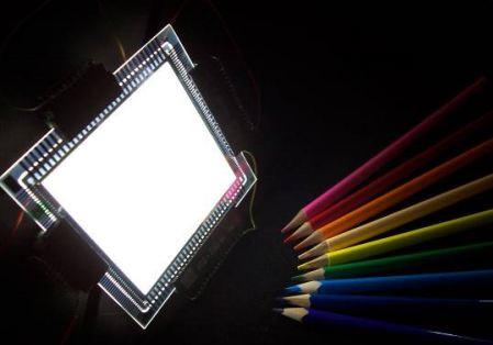
5 OLED TV 2012


6 OLED Lighting Status Quo and Why Photovoltaics?


7 Why Organic Photovoltaics? Why Organic Photovoltaics? USPs of OPV Flexible Preparation on PET/PEN foils Low temperature fabrication processes based on coating Adaptable in size and shape R2R or S2S fabrication: high throughput, low-cost, low investment cost Lightweight High absorption coefficient of acceptor materials (thin active PV layers nm) ~0,5 kg/m 2 Available in different color Available in (semi-) transparent form Short energy payback time Challenges on the way Solar cell efficiency Lifetime Cost of anode (ITO ) Fabrication process bridging the gap from the lab to the fab


8 Potential OPV Markets Leisure Required Efficiency Smart textiles Shading Consumer electronics Automotive & Transport RIPV Samsung Blue Earth Solarhandy Prototype ski jacket, Maier Sports PV marquee, Hymer Study Konarka Konarka BIPV Power plants Largest solar PV power plant of India BIPV - 'Palmenhouse' Munich Integrated Organic Sensor and Optoeletronics Technologies ISOTEC


 Elec.")


")
 NTC Weiz GmbH")
9 Transducers/Sensor Mechanisms using Hybrid MaPolymers Mechanical Parameters Pressure Frequency change Volume expansion Electrical Parameters Elec. Current (FET,OFET) Elec. Resistance Elec. Capacity Magnetic properties Optical Parameters Intensity Spectral Changes Lifetime of excited states.and many more Emil J.W. List Combining the Advantages and Disadvantages (Printed) Integrated Organic Sensor Devices + = (C) NTC Weiz GmbH Peter Pacher et al. patent pending; P. Pacher et al. Sensors and Actuators B 145, 181 (2010)

10 Integrated Organic Sensor and Optoelectronic Technologies ISOTEC (C) NTC Weiz GmbH Agenda Introduction Motivation What is Printed Electronics et Quo Vadis? Flexible Displays and Lighting Applications Plastic Photovoltaic Printed Smart Sensor Labels Inkjet Printing as an Industrial Production Process Conclusion
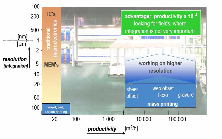


11 Productivity and resolution in printing technologies an overview Inkjet today Modified from (Source: Chemnitz University of Technology) Research Studio Austria INKJET FAB Optimization of the Magic Triangle of Inkjet-Printing for Obtaining Industrial Scale Printing Processes (Electronics, Solar, and Medical Applications, 2D and 3D) 0 = γ γ γ cos( Θ ) sv sl lv


 Photonic inks OSC, Dielectrics, etc.")
 Glass, Si-wafer PCBs")


 NTC Weiz GmbH Current Density")

12 Available Inkjet Processes Selected target applications: Conductive structures RFID antennas, ITO replacement Graphics, Solar applications Various inks: Metallic inks (Ag, Cu, Au, Pt, etc.) Photonic inks OSC, Dielectrics, etc. Qualified substrates: Flexible foils (PI, PET, PEN, etc) Glass, Si-wafer PCBs Paper, etc. Organic Solar Cell with Inkjet Printed Bottom Ag Electrodes ITO free bottom electrodes: Inkjet Printed Ag and spincast PEDOT-PSS Active layer: P3HT:PC 61 BM = 1:1 Performance: V oc = 0,58V I sc = 6,51mA/cm 2 FF = 47% Eff. = 1,77% (C) NTC Weiz GmbH Current Density (ma/cm²) A Elektrode = 1,5 cm² V OC = 0,58 V I SC = 6,51 ma/cm² FF = 47 % Eff = 1,77 % -5 dark illuminated -10-0,4-0,2 0,0 0,2 0,4 0,6 0,8 1,0 Bias (V)
 NTC Weiz GmbH Door handle with antibacterial hybrid polymer applied by means of spray coating Conclusion - Quo Vadis PE?")
13 Antibacterial Coatings Hybrid polymer with antibacterial properties Nontoxic when cured Scratch-resistant Transparent No growth of bacteria Broad field of applications Inkjet printable Tested on various substrates: Cu Al PVC PEN/PET Glass FR4 Si0 2 Paper (C) NTC Weiz GmbH Door handle with antibacterial hybrid polymer applied by means of spray coating Conclusion - Quo Vadis PE? OLED Display On market with smart phone displays (Samsung) Entering Market with TV (Samsung, LG, Sony?) OLED Lighting Entering the market in high end price segments OPV Entering market for consumer applications Status - R&D for BIPV and RIPV Memory and Logic Status R&D RFID and integrated Sensors etc. Status R&D Printed Battery Status R&D Poster, Smart Signage, and Billboard Status R&D


14 Thank You for Your Attention! Key Research Area at TU Graz: Advanced Materials Science Structure 14 Institutes from 4 Faculties Chemie, Physik, Bauingenieure, Maschinenbau NanoTecCenter Weiz Forschungsgesellschaft mbh Zentrum für Elektronenmikroskopie Graz 4 CD-Labors Materials Center Leoben K-net Fügetechnik


15 Key Research Area at TU Graz: Advanced Materials Science - Competences Synthesis Surface Science Characterization Modeling Device Fabrication Basic Research - Applied Research Technology Development Interdisciplinary Master: Advanced Materials Science Thank You for Your Attention!
National Centre for Flexible Electronics
 National Centre for Flexible Electronics Tripartite Partnership Government FlexE Centre - A platform for a meaningful interaction between industry and academia. An interdisciplinary team that advances
The Future for Printed Electronics
 The Future for Printed Electronics Jon Helliwell National Centre for Printable Electronics 24 October, 2013 Copyright CPI 2013. All rights reserved What is Printed Electronics? Organic and printed electronics
Advancing Consumer Packaging Through Printable Electronics
 IPST Executive Conference, Atlanta, GA March 9-10, 2011 Advancing Consumer Packaging Through Printable Electronics Bernard Kippelen Professor, School of Electrical and Computer Engineering Director, Center
Printable Organic Solar Cells Challenges and Opportunities in Technology Transfer from Lab to Market
 Power Plastic R Printable Organic Solar Cells Challenges and Opportunities in Technology Transfer from Lab to Market Alan J. Heeger Chief Scientist and Co-Founder 116 John Street, Lowell, MA 01852 Plastic
Accelerating Scale Up of Large Area Electronics
 Accelerating Scale Up of Large Area Electronics Duncan Lindsay Business Development Director, CPI 2015 Centre for Process Innovation Limited. All Rights Reserved. Who are CPI? CPI is a UK technology innovation
Flexible Electronics: Revolutionary Products and Career Opportunities for Creative Engineers
 Flexible Electronics: Revolutionary Products and Career Opportunities for Creative Engineers TAPPI - PIMA Student Summit 2011 Michael Ciesinski President January 15, 2011 Microelectronics changed the world
Printing Beyond Color. Printed Smart Objects on Advanced Paper Substrates. Reinhard R. Baumann
 Printing Beyond Color Printed Smart Objects on Advanced Paper Substrates June 17, 2009 member of Reinhard R. Baumann member of Chemnitz University of Technology Institute for Print and Media Technology
Low Temperature Integration of Thin Films and Devices for Flexible and Stretchable Electronics
 Low Temperature Integration of Thin Films and Devices for Flexible and Stretchable Electronics Pooran Joshi, Stephen Killough, and Teja Kuruganti Oak Ridge National Laboratory FIIW 2015 Displays and PV
 Organic and flexible Electronics in Saxony www.invest-in-saxony.com WElCOME Organic electronics are based on the discovery that specific organic materials possess semiconducting properties. Functional
Herzlich willkommen. Druckbare Sensoren für Food Packaging ICT-Agri-Food Symposium. Sören Fricke Section Head Large Area & Flexible Systems
 Herzlich willkommen Druckbare Sensoren für Food Packaging ICT-Agri-Food Symposium Sören Fricke Section Head Large Area & Flexible Systems Agroscope Tänikon, 05.09.2017 Motivation Printed Sensors can be
Analysis of Wet Coating Thickness Effect on Transparent Conductive Electrode Performance using Silver Nanowire
 Analysis of Wet Coating Thickness Effect on Transparent Conductive Electrode Performance using Silver Nanowire 2017. 04. 25 Seung-Hyun Lee, PhD Senior Researcher Dept. Printed Electronics Korea Institute
Printing versus coating technology Which way Printed Electronics with solution coating will go?
 Printing versus coating technology Which way Printed Electronics with solution coating will go? Frank Schäfer, Andrea Glawe, Dr. Daniel Eggerath, KROENERT GmbH& Co KG, Schuetzenstrasse 105, 22761 Hamburg
Processes for Flexible Electronic Systems
 Processes for Flexible Electronic Systems Michael Feil Fraunhofer Institut feil@izm-m.fraunhofer.de Outline Introduction Single sheet versus reel-to-reel (R2R) Substrate materials R2R printing processes
Solar Cell Parameters and Equivalent Circuit
 9 Solar Cell Parameters and Equivalent Circuit 9.1 External solar cell parameters The main parameters that are used to characterise the performance of solar cells are the peak power P max, the short-circuit
Holst Centre Wireless Autonomous Sensor Technologies & Flexible Electronics
 February 10, 2011 Holst Centre Wireless Autonomous Sensor Technologies & Flexible Electronics Presentation overview -General overview -Research focus < 4 Holst Centre: a solid partner in research Independent,
Здра вствуйте, това рищи!
 Manufacturing of Smart Objects by Printing Technologies Здра вствуйте, това рищи! Moscow / RUS, June 05, 2013 Reinhard R. Baumann Chemnitz University of Technology Chair of Digital Printing Fraunhofer
Additive & Inkjet Printing Technologies & Applications
 Additive & Inkjet Printing Technologies & Applications Debbie Thorp, Business Development Director Global Inkjet Systems Ltd Silverstone Park - October 2018 GIS Products DFE Atlas User Interface Machine
Heterogeneous integration of autonomous smart films based on electrochromic transistors
 of autonomous smart films NEWSLETTER #5 www.smartwww.smart-ec.eu Objectives SMART-EC has finalized last August 2014; it aimed at the development of self-powered electrochromic (EC) display device with
Printed Electronics Product Types & Markets. Vince Cahill, VCE Solutions
 Printed Electronics Product Types & Markets Vince Cahill, VCE Solutions Printed Electronic Product Types Printed circuits boards Printed logic / memory Printed batteries Membrane switches Photovoltaics
For personal use only
 Pooled Development Fund funding Australian SME owned projects in technology and resources. Specialty focus on backing projects with large scale upside potential. Maintain significant control over direction
Henkel solutions enabling printed electronics. Dr. Crystal Yang
 Henkel solutions enabling printed electronics Dr. Crystal Yang Agenda 1. Introduction Henkel 2. Trends in Printed Electronics 3. Novel materials enabling Printed Electronics New high speed printable silver
SILICON NANOWIRE HYBRID PHOTOVOLTAICS
 SILICON NANOWIRE HYBRID PHOTOVOLTAICS Erik C. Garnett, Craig Peters, Mark Brongersma, Yi Cui and Mike McGehee Stanford Univeristy, Department of Materials Science, Stanford, CA, USA ABSTRACT Silicon nanowire
10/14/2009. Semiconductor basics pn junction Solar cell operation Design of silicon solar cell
 PHOTOVOLTAICS Fundamentals PV FUNDAMENTALS Semiconductor basics pn junction Solar cell operation Design of silicon solar cell SEMICONDUCTOR BASICS Allowed energy bands Valence and conduction band Fermi
Light management in photovoltaics using nanotechnology
 Light management in photovoltaics using nanotechnology Albert Polman Center for Nanophotonics FOM-Institute AMOLF Amsterdam, The Netherlands Solar irradiance on earth assuming 30% PV, 175 W/m 2 Solar
A R&D cluster bringing thin film solar energy technology to excellence
 SOLLIANCE A R&D cluster bringing thin film solar energy technology to excellence Solliance OPV: Towards Low Cost, Efficient and Stable Organic Photovoltaic Modules Ronn Andriessen Solliance OPV Program
Printed Electronics: success stories and future commercial applications
 Printed Electronics: success stories and future commercial applications Dr Guillaume Chansin @gchansin June 2017 Helping you profit from emerging technologies Advantages of printed electronics Mass production
EU Research project proposals (call for Finnish companies)
") EU Research project proposals (call for Finnish companies) 11th EEMELI Workshop 29 th August 2012 Jukka Hast Research Professor VTT Technical Research Centre of Finland 04/10/2012 2 General ICT theme work
EU Research project proposals (call for Finnish companies) 11th EEMELI Workshop 29 th August 2012 Jukka Hast Research Professor VTT Technical Research Centre of Finland 04/10/2012 2 General ICT theme work
Printable, Novel CNT Inks with V2V Technology
 Printable, Novel CNT Inks with V2V Technology William J. Hurley, Jr., PhD Chasm Technologies, Inc. Canton, MA June 23, 2010 New England Nanomanufacturing Summit 1 Outline CHASM Overview Alliance with SWeNT
2nd Asian Physics Olympiad
 2nd Asian Physics Olympiad TAIPEI, TAIWAN Experimental Competition Thursday, April 26, 21 Time Available : 5 hours Read This First: 1. Use only the pen provided. 2. Use only the front side of the answer
Improving Organic Solar Cells
 Improving Organic Solar Cells Mike McGehee, Alex Mayer, Jack Parmer, Mike Rowell, Mark Topinka, George Burkhardt Stanford University Goals 15 % efficiency $30/m 2 20 year lifetime i Cover 1 % of the country
PRINTED ELECTRONICS TECHNOLOGIES
 PRINTED ELECTRONICS TECHNOLOGIES YEARS OF R&D DRIVEN BY CONTINUOUS INNOVATION HAVE POSITIONNED GGI SOLUTIONS AS A LEADER IN PRINTED ELECTRONICS TECHNOLOGIES 2 As a level 1 member of the Printable Electronics
We give vision to all surfaces Plastic Electronics Dresden.
 We give vision to all surfaces Plastic Electronics Dresden www.isorg.fr laurent.jamet@isorg.fr 1 When Printed Electronics meet Design, Usages and Brands for eye catching and appealing products Company
Aerosol Jet technology opportunities
 Aerosol Jet technology opportunities Jiří Navrátil 1. Introduction history and formation 2. Aerosol Jet system 2.1 System components 2.2 Inks and substrates 3. Application of Aerosol Jet technology 4.
Intel's 65 nm Logic Technology Demonstrated on 0.57 µm 2 SRAM Cells
 Intel's 65 nm Logic Technology Demonstrated on 0.57 µm 2 SRAM Cells Mark Bohr Intel Senior Fellow Director of Process Architecture & Integration Intel 1 What are We Announcing? Intel has fabricated fully-functional
MAPPER: High throughput Maskless Lithography
 MAPPER: High throughput Maskless Lithography Marco Wieland CEA- Leti Alterative Lithography workshop 1 Today s agenda Introduction Applications Qualification of on-tool metrology by in-resist metrology
Emerging Print Technologies & Applications
 Emerging Print Technologies & Applications By: Pivotal Resources USA, Inc. 2901 Richmond Road #353 Lexington, KY 40509 (859) 230-0093 2013 PRIMIR/NPES EMERGING PRINT TECHNOLOGIES & APPLICATIONS TABLE OF
Supplementary Materials for
 advances.sciencemag.org/cgi/content/full/4/9/eaau0920/dc1 Supplementary Materials for 2D titanium carbide (MXene) for wireless communication Asia Sarycheva, Alessia Polemi, Yuqiao Liu, Kapil Dandekar,
Theta (deg)
") Counts (a.u.) Supporting Information Comprehensive Evaluation of CuBi 2 O 4 as a Photocathode Material for Photoelectrochemical Water Splitting Sean P. Berglund, * Fatwa F. Abdi, Peter Bogdanoff, Abdelkrim
Counts (a.u.) Supporting Information Comprehensive Evaluation of CuBi 2 O 4 as a Photocathode Material for Photoelectrochemical Water Splitting Sean P. Berglund, * Fatwa F. Abdi, Peter Bogdanoff, Abdelkrim
PILOT LINE FOR LARGE-AREA PRINTING OF ELECTRONIC AND PHOTONIC DEVICES. Simon Perraud, Ph.D. Vice president for European affairs
 PILOT LINE FOR LARGE-AREA PRINTING OF ELECTRONIC AND PHOTONIC DEVICES Simon Perraud, Ph.D. Vice president for European affairs ABOUT LITEN Liten is the research institute of CEA devoted to clean energy
EU's contribution to research and innovation in Electronics
 EU's contribution to research and innovation in Electronics Henri.RAJBENBACH@ec.europa.eu Nikolaos.KYRLOGLOU@ec.europa.eu European Commission DG CONNECT (not legally binding presentation) SEMICON Europa-Flex
Multiband Solar Concentrator using Transmissive Dichroic Beamsplitting
 Multiband Solar Concentrator using Transmissive Dichroic Beamsplitting Jason H. Karp and Joseph E. Ford Photonics Systems Integration Lab University of California, San Diego Jacobs School of Engineering
Performance and Loss Analyses of High-Efficiency CBD-ZnS/Cu(In 1-x Ga x )Se 2 Thin-Film Solar Cells
Se 2 Thin-Film Solar Cells") Performance and Loss Analyses of High-Efficiency CBD-ZnS/Cu(In 1-x Ga x )Se 2 Thin-Film Solar Cells Alexei Pudov 1, James Sites 1, Tokio Nakada 2 1 Department of Physics, Colorado State University, Fort
Performance and Loss Analyses of High-Efficiency CBD-ZnS/Cu(In 1-x Ga x )Se 2 Thin-Film Solar Cells Alexei Pudov 1, James Sites 1, Tokio Nakada 2 1 Department of Physics, Colorado State University, Fort
Making a Material Difference
 Making a Material Difference Founded as a QinetiQ corporate investment in January 2002 Spun out in 2007 Locations: Rochester, NYS, USA (HQ and Production) Farnborough and Malvern, UK (R&D, Production and
Mass transfer with elastomer stamps for microled displays.
 Frontiers in Assembly Mass transfer with elastomer stamps for microled displays. Matt Meitl X-Celeprint, Inc. mmeitl@x-celeprint.com 1 The best materials for the best displays The materials identify the
Large Area, Flexible Electronics TWG. Chair: Dan Gamota, Jabil
 Large Area, Flexible Electronics TWG Chair: Dan Gamota, Jabil Large Area Flexible Electronics Roadmap History 09/2005 inemi Stakeholders identify Flexible Electronics as Future Growth Market and authorize
Lithography in our Connected World
 Lithography in our Connected World SEMI Austin Spring Forum TOP PAN P R INTING CO., LTD MATER IAL SOLUTIONS DIVISION Toppan Printing Co., LTD A Broad-Based Global Printing Company Foundation: January 17,
Hermetic Packaging Solutions using Borosilicate Glass Thin Films. Lithoglas Hermetic Packaging Solutions using Borosilicate Glass Thin Films
 Hermetic Packaging Solutions using Borosilicate Glass Thin Films 1 Company Profile Company founded in 2006 ISO 9001:2008 qualified since 2011 Headquarters and Production in Dresden, Germany Production
Microprobe-enabled Terahertz sensing applications
 Microprobe-enabled Terahertz sensing applications World of Photonics, Laser 2015, Munich Protemics GmbH Aachen, Germany Terahertz microprobing technology: Taking advantage of Terahertz range benefits without
Supporting Information
 Solution-processed Nickel Oxide Hole Injection/Transport Layers for Efficient Solution-processed Organic Light- Emitting Diodes Supporting Information 1. C 1s high resolution X-ray Photoemission Spectroscopy
Introduction to Photovoltaics
 Introduction to Photovoltaics PHYS 4400, Principles and Varieties of Solar Energy Instructor: Randy J. Ellingson The University of Toledo February 24, 2015 Only solar energy Of all the possible sources
End-of-line Standard Substrates For the Characterization of organic
 FRAUNHOFER INSTITUTe FoR Photonic Microsystems IPMS End-of-line Standard Substrates For the Characterization of organic semiconductor Materials Over the last few years, organic electronics have become
Unit 2 Semiconductor Devices. Lecture_2.5 Opto-Electronic Devices
 Unit 2 Semiconductor Devices Lecture_2.5 Opto-Electronic Devices Opto-electronics Opto-electronics is the study and application of electronic devices that interact with light. Electronics (electrons) Optics
Session 9.1 SID2010 May 25 th, Sep Lyu Jae Jin. Samsung Electronics
 Session 9.1 SID2010 May 25 th, 2010 Sep. 18. 2010 Lyu Jae Jin Samsung Electronics Contents 2 Application of LCDs Projection Type: LCD Projector, Projection TV Direct View Type: Smart-Phone, I-Pad, N-PC,
Application Overview: Simplified I/V Characterization of DC-DC Converters
 Application Overview: Simplified I/V Characterization of DC-DC Converters What is a SMU? Source measure units (SMUs) are an all-in-one solution for current voltage (I/V) characterization with the combined
shaping global nanofuture ULTRA-PRECISE PRINTING OF NANOMATERIALS
 shaping global nanofuture ULTRA-PRECISE PRINTING OF NANOMATERIALS WHO ARE WE? XTPL S.A. is a company operating in the nanotechnology segment. The interdisciplinary team of XTPL develops on a global scale
Plan Optik AG. Plan Optik AG PRODUCT CATALOGUE
 Plan Optik AG Plan Optik AG PRODUCT CATALOGUE 2 In order to service the high demand of wafers more quickly, Plan Optik provides off the shelf products in sizes from 2 up to 300mm diameter. Therefore Plan
Japan Barrier Society
 ISO/TC61/SC11/WG3 Pre NWIP Japan Barrier Society Agenda Background - Features and market trend of flexible electronics devices - High-barrier film as substrate of flexible electronics devices Conventional
MID Manufacturing Process.
 3D Aerosol Jet Printing An Emerging MID Manufacturing Process. Dr. Martin Hedges Neotech Services MTP, Nuremberg, Germany info@neotechservices.com Aerosol Jet Printing Aerosol Jet Process Overview Current
Complementary Organic Semiconductor and Metal Integrated Circuits
 Complementary Organic Semiconductor and Metal Integrated Circuits COSMIC will generate an organic CMOS technology platform from design to manufacturing level. COSMIC will produce highly complex lead applications
Volume 11 - Number 19 - May 2015 (66-71) Practical Identification of Photovoltaic Module Parameters
 Practical Identification of Photovoltaic Module Parameters") ISESCO JOURNAL of Science and Technology Volume 11 - Number 19 - May 2015 (66-71) Abstract The amount of energy radiated to the earth by the sun exceeds the annual energy requirement of the world population.
ISESCO JOURNAL of Science and Technology Volume 11 - Number 19 - May 2015 (66-71) Abstract The amount of energy radiated to the earth by the sun exceeds the annual energy requirement of the world population.
LAB V. LIGHT EMITTING DIODES
 LAB V. LIGHT EMITTING DIODES 1. OBJECTIVE In this lab you will measure the I-V characteristics of Infrared (IR), Red and Blue light emitting diodes (LEDs). Using a photodetector, the emission intensity
EPIC s landscape on PICs (visible, short- near- and mid- IR)
") EPIC s landscape on PICs (visible, short- near- and mid- IR) The Future Photonics Hub Industry Day 12 September 2016 Southampton Jose Pozo Director of Technology and Innovation EPIC jose.pozo@epic-assoc.com
EPIC s landscape on PICs (visible, short- near- and mid- IR) The Future Photonics Hub Industry Day 12 September 2016 Southampton Jose Pozo Director of Technology and Innovation EPIC jose.pozo@epic-assoc.com
Feature-level Compensation & Control
 Feature-level Compensation & Control 2 Sensors and Control Nathan Cheung, Kameshwar Poolla, Costas Spanos Workshop 11/19/2003 3 Metrology, Control, and Integration Nathan Cheung, UCB SOI Wafers Multi wavelength
Specialization in Microelectronics. Wang Qijie Nanyang Assistant Professor in EEE March 8, 2013
 Specialization in Microelectronics Wang Qijie Nanyang Assistant Professor in EEE qjwang@ntu.edu.sg March 8, 2013 Electronic Engineering Option Microelectronics What is it about? Study of semiconductor
Supplementary Information
 Supplementary Information A hybrid CMOS-imager with a solution-processable polymer as photoactive layer Daniela Baierl*, Lucio Pancheri, Morten Schmidt, David Stoppa, Gian-Franco Dalla Betta, Giuseppe
Plastic Electronics Market Development. by Mr. Ed van den Kieboom Executive Board Member Plastic Electronics Foundation
 Plastic Electronics Market Development by Mr. Ed van den Kieboom Executive Board Member Plastic Electronics Foundation Plastic Electronics Foundation Established April 2005 Private non profit organization
Effect of Silicon Nanowire on Crystalline Silicon Solar Cell Characteristics
 Journal of Ultrafine Grained and Nanostructured Materials https://jufgnsm.ut.ac.ir Vol. 49, No.1, June 2016, pp. 43-47 Print SSN: 2423-6845 Online SSN: 2423-6837 DO: 10.7508/jufgnsm.2016.01.07 Effect of
Welcome to the 30th Anniversary of the Graphic Art and Media Faculty HCMC University of Technologie and Education
 12/1/2017 1 Welcome to the 30th Anniversary of the Graphic Art and Media Faculty HCMC University of Technologie and Education 12/1/2017 2 Since not all of You will seek a future in Arts and Media, some
The Department of Advanced Materials Engineering. Materials and Processes in Polymeric Microelectronics
 The Department of Advanced Materials Engineering Materials and Processes in Polymeric Microelectronics 1 Outline Materials and Processes in Polymeric Microelectronics Polymeric Microelectronics Process
GLOBAL MARKETS, TECHNOLOGIES AND MATERIALS FOR THIN AND ULTRATHIN FILMS
 GLOBAL MARKETS, TECHNOLOGIES AND MATERIALS FOR THIN AND ULTRATHIN FILMS SMC057C August Margareth Gagliardi Project Analyst ISBN: 1-62296-338-5 BCC Research 49 Walnut Park, Building 2 Wellesley, MA 02481
OVERVIEW OF PLASTIC SUBSTRATES FOR PRINTED ELECTRONICS
 OVERVIEW OF PLASTIC SUBSTRATES FOR PRINTED ELECTRONICS Robert Rus:n Sr. Applica+on and Market Development Manager Special thanks to: Karl Rakos Bill MacDonald Melinex polyester film Mylar polyester film
Printed and Hybrid Integration
 Printed and Hybrid Integration Neil Chilton PhD Technical Director, Printed Electronics Limited, UK Neil.Chilton@PrintedElectronics.com Printed Electronics Limited (PEL) General Overview PEL was founded
Chapter 4. Impact of Dust on Solar PV Module: Experimental Analysis
 Chapter 4 Impact of Dust on Solar PV Module: Experimental Analysis 53 CHAPTER 4 IMPACT OF DUST ON SOLAR PV MODULE: EXPERIMENTAL ANALYSIS 4.1 INTRODUCTION: On a bright, sunny day the sun shines approximately
with sensors which see, taste and feel for machines, thus facilitating safe operation or even stand-alone operation of these devices.
 BMBF project KoSiF started - companies and researchers working together on flexible and autonomous sensor systems Sensory films - smart skin for machines Page 1 of 10 In industrial products as well as
Energy & Space. International Presentations
 Energy & Space International Presentations 2012-2013 Advanced Electronics 3D Printed Circuit Boards 3D Printed Circuit Boards for Solder-Free Printable Electronics 4x4 Vehicles Arduino WiFi Android Controllers
Ubiquitous Displays and Sensors Activating Surfaces with Flexible Electronics. Dean Baker, Director FlexEnable. APAC Innovation Summit 2016, Hong Kong
 Ubiquitous Displays and Sensors Activating Surfaces with Flexible Electronics Dean Baker, Director FlexEnable, Hong Kong Activating surfaces with flexible displays and sensors Flexible Plastic Displays
Please contact T E L : ~ 4.
 Please contact T E L : +82-32-623-6320~ 4 E-MAIL : sales@kortherm.co.kr jshuh@kortherm.co.kr 1. LASER SAMPLE TEST - To serve companies and individuals who need sample tests before buying new laser micromachining
Bayer MaterialScience Functional Films: Printed Polymer Electronics
 Bayer MaterialScience Functional Films: Printed Polymer Electronics Dr. Karsten Dierksen Bayer MaterialScience Head of Functional Films Printed Electronics & Functional Materials D-51368 Leverkusen, Tel.
Printed Electronics. Applications
 Printed Electronics Research Through University-Industry Partnerships Outline Background on Printed Electronics (PE) Corporate Partnerships Raytheon UMass Lowell Research Institute (RURI) Printed Electronics
LITE /LAB /SCAN /INLINE:
 Metis Metis LITE /LAB /SCAN/ INLINE Metis LITE /LAB /SCAN /INLINE: Spectral Offline and Inline Measuring System, using Integrating Sphere, for coatings on foils/web and on large size glasses To ensure
Supplementary Information
 DOI: 1.138/NPHOTON.212.19 Supplementary Information Enhanced power conversion efficiency in polymer solar cells using an inverted device structure Zhicai He, Chengmei Zhong, Shijian Su, Miao Xu, Hongbin
Precision Cold Ablation Material Processing using High-Power Picosecond Lasers
 Annual meeting Burgdorf Precision Cold Ablation Material Processing using High-Power Picosecond Lasers Dr. Kurt Weingarten kw@time-bandwidth.com 26 November 2009 Background of Time-Bandwidth Products First
2007-Novel structures of a MEMS-based pressure sensor
 C-(No.16 font) put by office 2007-Novel structures of a MEMS-based pressure sensor Chang-Sin Park(*1), Young-Soo Choi(*1), Dong-Weon Lee (*2) and Bo-Seon Kang(*2) (1*) Department of Mechanical Engineering,
What is the highest efficiency Solar Cell?
 What is the highest efficiency Solar Cell? GT CRC Roof-Mounted PV System Largest single PV structure at the time of it s construction for the 1996 Olympic games Produced more than 1 billion watt hrs. of
Laboratory 2: PV Module Current-Voltage Measurements
 Laboratory 2: PV Module Current-Voltage Measurements Introduction and Background The current-voltage (I-V) characteristic is the basic descriptor of photovoltaic device performance. A fundamental understanding
Innovations in Laser Technologies and European scale
 Vilnius Innovation Forum, 3-4 September, 2015 Innovations in Laser Technologies and European scale Dr. Gediminas Račiukaitis Head of Department of Laser Technologies Center for Physical Sciences and Technology
A Circuit Model for Polymer Solar Cells. Shamica Green. Faculty advisor: Dr. Selman Hershfield. Abstract
 A Circuit Model for Polymer Solar Cells Shamica Green Faculty advisor: Dr. Selman Hershfield Abstract In this simulation a polymer solar cell is modeled by resistors and diodes in a circuit. Voltage outputs
Smart Textronics: Adding Function from Fiber to Fabric 9 th November, Munich, Benjamin Mohr, Volker Lutz, Thomas Gries. RWTH, Peter Winandy
 Smart Textronics: Adding Function from Fiber to Fabric 9 th November, Munich, Benjamin Mohr, Volker Lutz, Thomas Gries RWTH, Peter Winandy 2 3 4 5 Fiber based solutions 4 you RWTH, Peter Winandy 7 8 Institut
Modelling and simulation of PV module for different irradiation levels Balachander. K Department of EEE, Karpagam University, Coimbatore.
 6798 Available online at www.elixirpublishers.com (Elixir International Journal) Electrical Engineering Elixir Elec. Engg. 43 (2012) 6798-6802 Modelling and simulation of PV module for different irradiation
Compact Solar Cell Ultra-Wideband Dipole Antenna
 Compact Solar Cell Ultra-Wideband Dipole Antenna Mina Danesh*, John R. Long High-Frequency Electronics Research Lab July 16, 2010 Delft University of Technology Challenge the future Outline Motivation
EMERGING INKJET PRINTING TECHNOLOGIES, APPLICATIONS AND GLOBAL MARKETS
 EMERGING INKJET PRINTING TECHNOLOGIES, APPLICATIONS AND GLOBAL MARKETS AVM091B November 2014 Andrew McWilliams Project Analyst ISBN: 1-56965-999-0 BCC Research 49 Walnut Park, Building 2 Wellesley, MA
IMI Labs Semiconductor Applications. June 20, 2016
 IMI Labs Semiconductor Applications June 20, 2016 Materials Are At the Core of Innovation in the 21st Century Weight Space Flexibility Heat Management Lightweight Energy Efficient Temperature Energy Efficient
Printable Electronics
 Printable Electronics Printable Electronics The Centre for Process Innovation From innovation to commercialisation The Centre for Process Innovation From innovation to commercialisation The High Value
Large Area Steady State Solar Simulator - Apollo
 AllReal APOLLO series steady-state solar simulator are AAA class which is the highest class on the world. AllReal APOLLO solar simulators designed with specific optical technology by tandem Xenon lamps,
Radial Coupling Method for Orthogonal Concentration within Planar Micro-Optic Solar Collectors
 Radial Coupling Method for Orthogonal Concentration within Planar Micro-Optic Solar Collectors Jason H. Karp, Eric J. Tremblay and Joseph E. Ford Photonics Systems Integration Lab University of California
Silicon sensors for radiant signals. D.Sc. Mikko A. Juntunen
 Silicon sensors for radiant signals D.Sc. Mikko A. Juntunen 2017 01 16 Today s outline Introduction Basic physical principles PN junction revisited Applications Light Ionizing radiation X-Ray sensors in
Future battery technologies FET Flagship
 Future battery technologies FET Flagship BATTERY 2030+ initiative coordinator: Prof. Kristina Edström, Uppsala University, Sweden Deputy coordinator: Dr. Simon Perraud, CEA, France November 16, 2018 Batteries
write-nanocircuits Direct-write Jaebum Joo and Joseph M. Jacobson Molecular Machines, Media Lab Massachusetts Institute of Technology, Cambridge, MA
 Fab-in in-a-box: Direct-write write-nanocircuits Jaebum Joo and Joseph M. Jacobson Massachusetts Institute of Technology, Cambridge, MA April 17, 2008 Avogadro Scale Computing / 1 Avogadro number s? Intel
Welcome Shareholders Annual Meeting. FY2014 March 1, 2013 February 28, 2014
 Welcome Shareholders 2014 Annual Meeting March 1, 2013 February 28, 2014 1 Safe Harbor Statement This presentation contains forward-looking statements within the meaning of safe-harbor provisions of the
The Relationship Between Energy Gab & Efficiency in Dye Solar Cells
 e-issn 2455 1392 Volume 2 Issue 7, July 2016 pp. 82 89 Scientific Journal Impact Factor : 3.468 http://www.ijcter.com The Relationship Between Energy Gab & Efficiency in Dye Solar Cells 1 Sakina Ibrahim