Processes for Flexible Electronic Systems
|
|
|
- Tracey Wade
- 5 years ago
- Views:
Transcription

1 Processes for Flexible Electronic Systems Michael Feil Fraunhofer Institut
2 Outline Introduction Single sheet versus reel-to-reel (R2R) Substrate materials R2R printing processes R2R fine conductor lines R2R integration of active components Conclusion


3 Today Trends in Electronic Applications Tomorrow Logitech Fraunhofer Casio Infineon Philips Research


4 Electronic Goes Flexible Flexible Electronic Systems Advantages of flexible electronics rigid freedom in design cheap foil substrates light-weight compact portable products cost-effective assembly with reel-to-reel processing environment-friendly ubiquitous applications rigid-flex full flexible


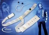
5 EU IP Project SHIFT - Smart High-Integration Flex embedded chip capacitive layer embedded IPD antenna integrated resistor
6 Single sheet production Characteristics Typically for standard PCBs, From cassette to cassette handling, Transport inside of a machine via belts and/or rolls All processes from flex circuit board up to the assembled and finished system possible Advantages: Multilayer easier and with better accuracy producible, Some assembly and curing processes simpler Critical points: - Handling of thin foil substrates, the thinner the more difficult, - Fixing on a rigid temporary carrier needed, - High throughput
7 Reel-to-reel (R2R) Characteristics Increase of throughput from stop and go to continuously working processes rotatory principles e.g. printing methods from flatbed screen printing to offset printing (paper industry) At the moment mainly used for single layer processing R2R assembly used for smart labels, Vacuum processes may, but must not be expensive (cigarette paper) Force free web transport Advantages: Very fast continuously running processes possible (from m/min to some m/s) Easier handling of thin foils Critical points: - Unexpected belt stop (especially at thermal processes), - Electrostatic charge - Layer to layer adjustment with high accuracy
8 Substrate materials Important parameters: Cost Mechanical Characteristics Thermal stability (solder processes at > 240 C) Moisture absorption Warpage resistant, shrinkage Coefficient of thermal expansion (CTE) Isotropy of the material Surface tension, wettability (adhesion) Chemicals resistant Biocompatibility Electrical Characteristics Dielectric coefficient (typ. 3 4) Loss angle (typ. 0,01 0,001) Voltage stability (typ. some kv at 50μm substrate thickness) Spec. resistance (typ. >10 16 Ωcm), surface resistance (typ. > Ωcm)
9 Low Cost Materials Flexible Electronic Systems Lower thermal stability, improvable by special treatment T g <100 C Polyester (PET) Standard material for smart label, good chem. resistance, max. process temperature: 120 C, medium moisture absorption (0,5%), lowest price PET thermal stabilized good chem. resistance, max. process temperature: 150 C, Polyethylen-naphtalat good chem. resistance, max. process temperature: 160 C, relatively (PEN) low-priced Temperature resistant substrates Polyimid (PI) Standard material for flex boards, good chem. resistance (alcali!), max. process temperature: > 280 C, medium moisture absorption (0,8%), high price Liquid Crystalline Polymer relatively new material especially for high frequency applications (LCP) very high chem. resistance, max. process temperature: 280 C, very low moisture absorption (0,04%), high price
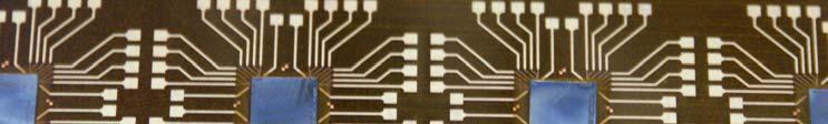
10 Modules of the Reel-to-Reel Application Center Substrate Technology Direct Metallization System Alignement Screen Printing Curing Resist Coating Development Standard Substrates Assembly Technology Bonding Module Fine-Pitch Substrates Etiching, Stripping Screen Printing Dispensing Die-Attach FC-Bonding Curing Laminator El. Test Laser treatment
 2.")


11 R2R Screen Printing, Example: Electroluminescent Pastes Structure of the display Process steps 1. Substrate (PET) 2. Print of bottom electrode, Ag paste ca. 10μm 3. 2 Prints of isolating layers, dielectric paste 20μm 4. Print of luminescent material, 35μm (3 colors possible) 5. Print of transparent electrode,10μm 6. Lamination of cover foil cover foil transparent electrode luminescent material dielectric layers bottom electrode substrate


12 R2R screen printing processes used in SHIFT 2-layer process Print of dielectric layer Min. size of printed via openings: 200μm Via openings by laser: μm Second conductor layer by screen printing Substrate Layer 2: Polymer Ag paste Dielectric layer Layer 1: Cu
 and ESL R12114 (10 kω/ )")

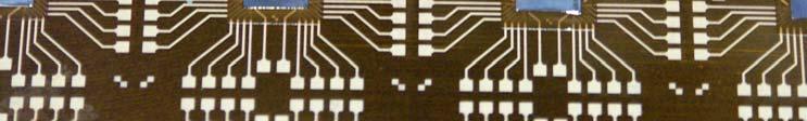
13 Integration of printed resistors ESL R12112 (100 Ω/ ) and ESL R12114 (10 kω/ ) L/W between 0.33 and 10 Minimal dimensions: 0.5 mm thermal treatment at 150 C up to 2h
14 R2R fine conductor lines Process flow subtractive technique (Cleaning) Lamination of photo resist (15μm solid resist, 15μm Mylar cover foil) Exposure (vacuum contact) Develop of photo resist Cu etch Removal of photo resist Process flow semiadditive technique (Cleaning) Lamination of photo resist (15μm solid resist, 15μm Mylar cover foil) Exposure (vacuum contact) Develop of photo resist Electro plating of Cu up to the desired thickness Removal of photo resist Cu difference etching


15 Fine pitch substrates Subtractive technique: 5μm Cu Semiadditive technique: 6-7μm Cu Interdigital test pattern, 40μm pitch Interdigital test pattern, 30μm pitch


 Need of adapted assembly methods 3-Punkt-Biegetest")
16 R2R integration of active components Ultra thin silicon becomes bendable ideal for application in ultra thin flexible systems Base material = monocrystalline Si brittle material adequate handling Dicing by thinning process (DbyT) using dry Si etching nearly ideal chip edges for highest breakage resistance DbyT allows any chip geometry (circle, polygone, rounded corners, etc.) Need of adapted assembly methods 3-Punkt-Biegetest Biegeradius ca. 2mm!
17 Manufacture and transfer of 20 μm thin chips according to Dicing-by-Thinning concept Device wafer Device wafer Carrier wafer Device wafer Carrier wafer Device wafer having dryetched chip grooves Laminate double side adhesive tape; combination of temperature- and UVreleasable tape Bonding of device and carrier wafer under vacuum conditions; Waferstack ready for thinning Carrier wafer Backside thinning ( grinding, etching)until front side grooves are opened Remove chip / tape ensemble by heating; Transfer of chips onto pick-up tape Removal of tape Chips ready for pick&place
18 Assembly and Electrical Interconnection Methods for Thin Chips Face Up Assembly and Isoplanar Contacts Face Down Assembly FC-like Technique Contacts across chip edge Contacts through laminated foil Contacts through coated film ACA ICA /NCA ICA Solder


19 Pick and Place of 20 μm Thin Chips Process is based on: Dicing-by-Thinning concept using dryetched grooves Pick & place process using thermal releasable tapes IC local heating Automated, fast pick-up process for μm thin chips developed by Mühlbauer Principle of thermal releasable connection


 Pitch depending on print method Cross-section of an")
20 Isoplanar Interconnection Technique NCA IC Conductor line IC Substrate Curing Substrate ICA Due to low topography of thin ICs, electrical interconnection is achieved by printing or dispensing of silver-filled polymer across chip edge Pressure less method Lowest total system thickness (thickness of conductor line does not contribute to the assembly height of IC) Pitch depending on print method Cross-section of an Isoplanar Contact source: Epson


21 Flip Chip Bonding Technique with ACA bumps IC substrate bonding force ACA conductor after placement curing with continuous bonding force IC substrate Flip Chip with ACA: Low resistance State of the art High pin count Narrow pitches


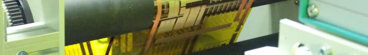


22 Reel-to-reel (R2R) assembly of thin chip


23 Ultrathin soldered Flip Chip Interconnections Chips: Contact: Flex: min. thickness: 20 μm size: 5 x 5 mm2, pitch: 100 μm 3 μm SnCu PI 25 μm, Cu 10 μm epoxy+ Kapton each 25 μm Barbara Pahl, Berlin

24 Ultra thin foil package 6 2, Substrate: PET/Polyimide 2. Metallization: Cu 3. Cu Patterning: Litho/etching 4. ACA deposition/ chip placement 5. Screen printing dielectric layer 6. Screen printing of Ag paste or Cu-technique

25 Demonstrator for Film Package Flexible Electronic Systems Combination of Flat Battery, IC (SMD) and display Integrated with cold assembly steps Further integration with solar cell and charging circuit
26 Conclusion In future, flexible electronic systems have a very high application potential This requires thin flexible foils as substrates In view of cost and handling of thin foils, R2R processes are the right choice Need of integration methods of various elements like active and passive elements, sensors, power supply, etc. with adequate mechanical properties and geometrical dimensions Many methods are working in a laboratory scale, but from production point of view there is something to do In this field, the Fraunhofer with his R2R application center is a competent partner for the industry
Ultra-thin, highly flexible RF cables and interconnections
 Ultra-thin, highly flexible RF cables and interconnections Hans Burkard, Hightec MC AG, Lenzburg, Switzerland Urs Brunner, Hightec MC AG, Lenzburg, Switzerland Karl Kurz, Hightec MC AG, Lenzburg, Switzerland
Ultra-Thin, Highly Flexible Cables and Interconnections for Low and High Frequencies
 Ultra-Thin, Highly Flexible Cables and Interconnections for Low and High Frequencies Hans Burkard a, Tobias Lamprecht b, Thomas Morf b, Bert Jan Offrein b, Josef Link a a Hightec MC AG, Fabrikstrasse,
NEW PACKAGING AND INTERCONNECT TECHNOLOGIES FOR ULTRA THIN CHIPS
 NEW PACKAGING AND INTERCONNECT TECHNOLOGIES FOR ULTRA THIN CHIPS Christine Kallmayer and Rolf Aschenbrenner Fraunhofer IZM Berlin, Germany kallmayer@izm.fhg.de Julian Haberland and Herbert Reichl Technical
Chapter 11 Testing, Assembly, and Packaging
 Chapter 11 Testing, Assembly, and Packaging Professor Paul K. Chu Testing The finished wafer is put on a holder and aligned for testing under a microscope Each chip on the wafer is inspected by a multiple-point
Large area cost-efficient electronics integration. Flexible Substrate Polytronische Systeme
 Large area cost-efficient electronics integration. Flexible Substrate Polytronische Systeme Institut Zuverlässigkeit und Mikrointegration Institutsteil München Karlheinz Bock for Hansastr. 27d, D-80686
Advanced High-Density Interconnection Technology
 Advanced High-Density Interconnection Technology Osamu Nakao 1 This report introduces Fujikura s all-polyimide IVH (interstitial Via Hole)-multi-layer circuit boards and device-embedding technology. Employing
Fraunhofer IZM - ASSID
 FRAUNHOFER-INSTITUT FÜR Zuverlässigkeit und Mikrointegration IZM Fraunhofer IZM - ASSID All Silicon System Integration Dresden Heterogeneous 3D Wafer Level System Integration 3D system integration is one
Chip Assembly on MID (Molded Interconnect Device) A Path to Chip Modules with increased Functionality
 A Path to Chip Modules with increased Functionality") T e c h n o l o g y Dr. Werner Hunziker Chip Assembly on MID (Molded Interconnect Device) A Path to Chip Modules with increased Functionality The MID (Molded Interconnect Device) technology enables the
T e c h n o l o g y Dr. Werner Hunziker Chip Assembly on MID (Molded Interconnect Device) A Path to Chip Modules with increased Functionality The MID (Molded Interconnect Device) technology enables the
Tape Automated Bonding
 Tape Automated Bonding Introduction TAB evolved from the minimod project begun at General Electric in 1965, and the term Tape Automated Bonding was coined by Gerard Dehaine of Honeywell Bull in 1971. The
B. Flip-Chip Technology
 B. Flip-Chip Technology B1. Level 1. Introduction to Flip-Chip techniques B1.1 Why flip-chip? In the development of packaging of electronics the aim is to lower cost, increase the packaging density, improve
Advanced Packaging - Pulsed-laser Heating for Flip Chip Assembly
 Page 1 of 5 Pulsed-laser Heating for Flip Chip Assembly A stress-free alternative By Thorsten Teutsch, Ph.D., Pac Tech USA, Elke Zakel, Ph.D., and Ghassem Azdasht, Pac Tech GmbH As flip chip applications
Application Bulletin 240
 Application Bulletin 240 Design Consideration CUSTOM CAPABILITIES Standard PC board fabrication flexibility allows for various component orientations, mounting features, and interconnect schemes. The starting
Thin Film Resistor Integration into Flex-Boards
 Thin Film Resistor Integration into Flex-Boards 7 rd International Workshop Flexible Electronic Systems November 29, 2006, Munich by Dr. Hans Burkard Hightec H MC AG, Lenzburg, Switzerland 1 Content HiCoFlex:
Hermetic Packaging Solutions using Borosilicate Glass Thin Films. Lithoglas Hermetic Packaging Solutions using Borosilicate Glass Thin Films
 Hermetic Packaging Solutions using Borosilicate Glass Thin Films 1 Company Profile Company founded in 2006 ISO 9001:2008 qualified since 2011 Headquarters and Production in Dresden, Germany Production
Flexible Hybrid Electronics Fabricated with High-Performance COTS ICs using RTI CircuitFilm TM Technology
 Flexible Hybrid Electronics Fabricated with High-Performance COTS ICs using RTI CircuitFilm TM Technology Scott Goodwin 1, Erik Vick 2 and Dorota Temple 2 1 Micross Advanced Interconnect Technology Micross
Active and passive component embedding into low-cost plastic substrates aimed at smart system applications
 Active and passive component embedding into low-cost plastic substrates aimed at smart system applications Maarten Cauwe 1, Bjorn Vandecasteele 1, Johan De Baets 1, Jeroen van den Brand 2, Roel Kusters
EMERGING SUBSTRATE TECHNOLOGIES FOR PACKAGING
 EMERGING SUBSTRATE TECHNOLOGIES FOR PACKAGING Henry H. Utsunomiya Interconnection Technologies, Inc. Suwa City, Nagano Prefecture, Japan henryutsunomiya@mac.com ABSTRACT This presentation will outline
!"#$"%&' ()#*+,-+.&/0(
#*+,-+.&/0(") !"#$"%&' ()#*+,-+.&/0( Multi Chip Modules (MCM) or Multi chip packaging Industry s first MCM from IBM. Generally MCMs are horizontal or two-dimensional modules. Defined as a single unit containing two
!"#$"%&' ()#*+,-+.&/0( Multi Chip Modules (MCM) or Multi chip packaging Industry s first MCM from IBM. Generally MCMs are horizontal or two-dimensional modules. Defined as a single unit containing two
CHAPTER 11: Testing, Assembly, and Packaging
 Chapter 11 1 CHAPTER 11: Testing, Assembly, and Packaging The previous chapters focus on the fabrication of devices in silicon or the frontend technology. Hundreds of chips can be built on a single wafer,
Die Prep Considerations for IC Device Applications CORWIL Technology 1635 McCarthy Blvd Milpitas, CA 95035
 Die Prep Considerations for IC Device Applications CORWIL Technology 1635 McCarthy Blvd Milpitas, CA 95035 Jonny Corrao Die Prep While quality, functional parts are the end goal for all semiconductor companies,
Mobile Electrostatic Carrier (MEC) evaluation for a GaAs wafer backside manufacturing process
 evaluation for a GaAs wafer backside manufacturing process") Mobile Electrostatic Carrier (MEC) evaluation for a GaAs wafer backside manufacturing process H.Stieglauer 1, J.Nösser 1, A.Miller 1, M.Lanz 1, D.Öttlin 1, G.Jonsson 1, D.Behammer 1, C.Landesberger 2,
Mobile Electrostatic Carrier (MEC) evaluation for a GaAs wafer backside manufacturing process H.Stieglauer 1, J.Nösser 1, A.Miller 1, M.Lanz 1, D.Öttlin 1, G.Jonsson 1, D.Behammer 1, C.Landesberger 2,
Lecture: Integration of silicon photonics with electronics. Prepared by Jean-Marc FEDELI CEA-LETI
 Lecture: Integration of silicon photonics with electronics Prepared by Jean-Marc FEDELI CEA-LETI Context The goal is to give optical functionalities to electronics integrated circuit (EIC) The objectives
Data Sheet _ R&D. Rev Date: 8/17
 Data Sheet _ R&D Rev Date: 8/17 Micro Bump In coming years the interconnect density for several applications such as micro display, imaging devices will approach the pitch 10um and below. Many research
Printing versus coating technology Which way Printed Electronics with solution coating will go?
 Printing versus coating technology Which way Printed Electronics with solution coating will go? Frank Schäfer, Andrea Glawe, Dr. Daniel Eggerath, KROENERT GmbH& Co KG, Schuetzenstrasse 105, 22761 Hamburg
Brief Introduction of Sigurd IC package Assembly
 Brief Introduction of Sigurd IC package Assembly Content Package Development Trend Product Brief Sawing type QFN Representative MEMS Product LGA Light Sensor Proximity Sensor High Yield Capability Low
Dicing Through Hard and Brittle Materials in the Micro Electronic Industry By Gideon Levinson, Dicing Tools Product Manager
 Dicing Through Hard and Brittle Materials in the Micro Electronic Industry By Gideon Levinson, Dicing Tools Product Manager A high percentage of micro electronics dicing applications require dicing completely
MASW P. SURMOUNT PIN Diode Switch Element with Thermal Terminal. Features. Description. Ordering Information 2.
 Features Specified Bandwidth: 45MHz 2.5GHz Useable 30MHz to 3.0GHz Low Loss 40dB High C.W. Incident Power, 50W at 500MHz High Input IP3, +66dBm @ 500MHz Unique Thermal Terminal for
PANEL LEVEL PACKAGING A MANUFACTURING SOLUTION FOR COST-EFFECTIVE SYSTEMS
 PANEL LEVEL PACKAGING A MANUFACTURING SOLUTION FOR COST-EFFECTIVE SYSTEMS R. Aschenbrenner, K.-F. Becker, T. Braun, and A. Ostmann Fraunhofer Institute for Reliability and Microintegration Berlin, Germany
Printed and Hybrid Integration
 Printed and Hybrid Integration Neil Chilton PhD Technical Director, Printed Electronics Limited, UK Neil.Chilton@PrintedElectronics.com Printed Electronics Limited (PEL) General Overview PEL was founded
Analysis of Wet Coating Thickness Effect on Transparent Conductive Electrode Performance using Silver Nanowire
 Analysis of Wet Coating Thickness Effect on Transparent Conductive Electrode Performance using Silver Nanowire 2017. 04. 25 Seung-Hyun Lee, PhD Senior Researcher Dept. Printed Electronics Korea Institute
SOLDER BUMP FLIP CHIP BONDING FOR PIXEL DETECTOR HYBRIDIZATION
 SOLDER BUMP FLIP CHIP BONDING FOR PIXEL DETECTOR HYBRIDIZATION Jorma Salmi and Jaakko Salonen VTT Information Technology Microelectronics P.O. Box 1208 FIN-02044 VTT, Finland (visiting: Micronova, Tietotie
Laser Assisted Flip Chip Assembly for LCD Applications using ACP and NCP Adhesive Joining
 1 Laser Assisted Flip Chip Assembly for LCD Applications using ACP and NCP Adhesive Joining Elke Zakel, Ghassem Azdasht, Thorsten Teutsch *, Ronald G. Blankenhorn* Pac Tech Packaging Technologies GmbH
Technology development for a flexible, low-cost backplane for lighting applications
 IMAPS-Benelux Spring Event 2014 Technology development for a flexible, low-cost backplane for lighting applications M. Cauwe 1, A. Sridhar 2, T. Sterken 1 1 imec - Cmst, Technologiepark, Zwijnaarde, Belgium
Flip-Chip for MM-Wave and Broadband Packaging
 1 Flip-Chip for MM-Wave and Broadband Packaging Wolfgang Heinrich Ferdinand-Braun-Institut für Höchstfrequenztechnik (FBH) Berlin / Germany with contributions by F. J. Schmückle Motivation Growing markets
High Frequency Single & Multi-chip Modules based on LCP Substrates
 High Frequency Single & Multi-chip Modules based on Substrates Overview Labtech Microwave has produced modules for MMIC s (microwave monolithic integrated circuits) based on (liquid crystal polymer) substrates
PRINTED ELECTRONICS 3
 PRINTED ELECTRONICS 3 4 INKTEC PRINTED ELECTRONICS 5 6 INKTEC PRINTED ELECTRONICS 7 InkTec Leads New Paradigm in Printed Electronic Materials Applications OTFT, Memory Cell, Display, RFID and so on Product
Through Glass Via (TGV) Technology for RF Applications
 Technology for RF Applications") Through Glass Via (TGV) Technology for RF Applications C. H. Yun 1, S. Kuramochi 2, and A. B. Shorey 3 1 Qualcomm Technologies, Inc. 5775 Morehouse Dr., San Diego, California 92121, USA Ph: +1-858-651-5449,
Through Glass Via (TGV) Technology for RF Applications C. H. Yun 1, S. Kuramochi 2, and A. B. Shorey 3 1 Qualcomm Technologies, Inc. 5775 Morehouse Dr., San Diego, California 92121, USA Ph: +1-858-651-5449,
Innovative pcb solutions used in medical and other devices Made in Switzerland
 Innovative pcb solutions used in medical and other devices Made in Switzerland Chocolate Watches Money.PCB`s innovative pcb`s... Customer = innovation driver Need to add more parts and I/O make smaller/thinner
Diverse Lasers Support Key Microelectronic Packaging Tasks
 Diverse Lasers Support Key Microelectronic Packaging Tasks Written by D Muller, R Patzel, G Oulundsen, H Halou, E Rea 23 July 2018 To support more sophisticated and compact tablets, phones, watches and
David B. Miller Vice President & General Manager September 28, 2005
 Electronic Technologies Business Overview David B. Miller Vice President & General Manager September 28, 2005 Forward Looking Statement During the course of this meeting we may make forward-looking statements.
Chapter 2. Literature Review
 Chapter 2 Literature Review 2.1 Development of Electronic Packaging Electronic Packaging is to assemble an integrated circuit device with specific function and to connect with other electronic devices.
New fabrication and packaging technologies for CMOS pixel sensors: closing gap between hybrid and monolithic
 New fabrication and packaging technologies for CMOS pixel sensors: closing gap between hybrid and monolithic Outline Short history of MAPS development at IPHC Results from TowerJazz CIS test sensor Ultra-thin
Multilayer Foil Metallization for All Back Contact Cells
 Multilayer Foil Metallization for All Back Contact Cells David Levy, Natcore Technology David Carlson, CarlsonPV 44 th IEEE-PVSC Conference (June 30, 2017) 1 Overview Multilayer foil metallization Benefits
Printing Beyond Color. Printed Smart Objects on Advanced Paper Substrates. Reinhard R. Baumann
 Printing Beyond Color Printed Smart Objects on Advanced Paper Substrates June 17, 2009 member of Reinhard R. Baumann member of Chemnitz University of Technology Institute for Print and Media Technology
Flexline - A Flexible Manufacturing Method for Wafer Level Packages (Extended Abstract)
") Flexline - A Flexible Manufacturing Method for Wafer Level Packages (Extended Abstract) by Tom Strothmann, *Damien Pricolo, **Seung Wook Yoon, **Yaojian Lin STATS ChipPAC Inc.1711 W Greentree Drive Tempe,
Flexline - A Flexible Manufacturing Method for Wafer Level Packages (Extended Abstract) by Tom Strothmann, *Damien Pricolo, **Seung Wook Yoon, **Yaojian Lin STATS ChipPAC Inc.1711 W Greentree Drive Tempe,
64 Channel Flip-Chip Mounted Selectively Oxidized GaAs VCSEL Array
 64 Channel Flip-Chip Mounted Selectively Oxidized GaAs VCSEL Array 69 64 Channel Flip-Chip Mounted Selectively Oxidized GaAs VCSEL Array Roland Jäger and Christian Jung We have designed and fabricated
Benzocyclobutene Polymer dielectric from Dow Chemical used for wafer-level redistribution.
 Glossary of Advanced Packaging: ACA Bare Die BCB BGA BLT BT C4 CBGA CCC CCGA CDIP or CerDIP CLCC COB COF CPGA Anisotropic Conductive Adhesive Adhesive with conducting filler particles where the electrical
Bend Sensor Technology Mechanical Application Design Guide Mechanical Application Design Guide
 Bend Sensor Technology Mechanical Application Design Guide Mechanical Application Design Guide www.flexpoint.com Copyright 2015 Flexpoint Sensor Systems Page 1 of 10 2 Bend Sensor Technology Mechanical
Flip Chip Bonding Using Sony Anisotropic Conductive Film (ACF) FP1526Y
 FP1526Y") Flip Chip Bonding Using Sony Anisotropic Conductive Film (ACF) FP1526Y Purpose: Author: Rekha S. Pai (07/29/03) To use ACF as an interconnection method for attaching dice to substrates. Direct electrical
Flip Chip Bonding Using Sony Anisotropic Conductive Film (ACF) FP1526Y Purpose: Author: Rekha S. Pai (07/29/03) To use ACF as an interconnection method for attaching dice to substrates. Direct electrical
Thinning of IC chips
 1 Thinning of IC chips Annette Teng CORWIL TECHNOLOGY CORP. 1635 McCarthy Blvd. Milpitas, CA 95135 2 CONTENT Industry Demand for thinness Method to achieve ultrathin dies Mechanical testing of ultrathin
Min Tao, Ph. D, Ashok Prabhu, Akash Agrawal, Ilyas Mohammed, Ph. D, Bel Haba, Ph. D Oct , IWLPC
 PACKAGE-ON-PACKAGE INTERCONNECT FOR FAN-OUT WAFER LEVEL PACKAGES Min Tao, Ph. D, Ashok Prabhu, Akash Agrawal, Ilyas Mohammed, Ph. D, Bel Haba, Ph. D Oct 18-20 2016, IWLPC 1 Outline Laminate to Fan-Out
PAGE 1/6 ISSUE Jul SERIES Micro-SPDT PART NUMBER R516 XXX 10X R 516 _ 1 0 _
 PAGE 1/6 ISSUE Jul-24-2017 SERIES Micro-SPDT PART NUMBER R516 XXX 10X R516 series: the RAMSES concept merges with the SLIM LINE technology, breaking up the frequency limits of SMT switches : - FULL SMT
Plan Optik AG. Plan Optik AG PRODUCT CATALOGUE
 Plan Optik AG Plan Optik AG PRODUCT CATALOGUE 2 In order to service the high demand of wafers more quickly, Plan Optik provides off the shelf products in sizes from 2 up to 300mm diameter. Therefore Plan
 Distributed by: www.jameco.com -800-83-4242 The content and copyrights of the attached material are the property of its owner. HPND- 4005 Beam Lead PIN Diode Data Sheet Description The HPND-4005 planar
Advanced Packaging Equipment Solder Jetting & Laser Bonding
 Advanced Packaging Equipment Solder Jetting & Laser Bonding www.pactech.comw.pactech.com PacTech Packaging Technologies Pioneering in laser solder jetting technologies since 1995 Our mission is to reshape
An Introduction to Electronics Systems Packaging. Prof. G. V. Mahesh. Department of Electronic Systems Engineering
 An Introduction to Electronics Systems Packaging Prof. G. V. Mahesh Department of Electronic Systems Engineering India Institute of Science, Bangalore Module No. # 02 Lecture No. # 08 Wafer Packaging Packaging
MADP Solderable AlGaAs Flip Chip PIN. Features. Chip Dimensions. Description. Applications
 Features Low Series Resistance Ultra Low Capacitance Millimeter Wave Switching & Cutoff Frequency 2 Nanosecond Switching Speed Can be Driven by a Buffered TTL Silicon Nitride Passivation Polyimide Scratch
ACTIVE IMPLANTS. Glass Encapsulation
 ACTIVE IMPLANTS Glass Encapsulation OUTLINE Smart Implants Overview Cylindrical Glass Encapsulation CGE Planar Glass Encapsulation PGE Platform for Innovative Implantable Devices 5/7/2013 Glass Encapsulation
MicroSiP TM DC/DC Converters Fully Integrated Power Solutions
 MicroSiP TM DC/DC Converters Fully Integrated Power Solutions PicoStar TM Christophe Vaucourt Thies Puchert, Udo Ottl, Frank Stepniak, Florian Feckl 1 Outline Illustrate TI s recent developments in the
HipoCIGS: enamelled steel as substrate for thin film solar cells
 HipoCIGS: enamelled steel as substrate for thin film solar cells Lecturer D. Jacobs*, Author S. Efimenko, Co-author C. Schlegel *:PRINCE Belgium bvba, Pathoekeweg 116, 8000 Brugge, Belgium, djacobs@princecorp.com
Assembly/Packagng RF-PCB. Thick Film. Thin Film. Screening/Test. Design Manual
 Thick Film Thin Film RF-PCB Assembly/Packagng Screening/Test Design Manual RHe Design Manual The following rules are effective for the draft of circuit boards and hybrid assemblies. The instructions are
"CONDUCTIVE ADHESIVES THE HIGH TECH SOLUTION IN MEDICAL ELECTRONICS" By Dr. Ken Gilleo, Ph.D. 1 & Bob Boyes 2
 "CONDUCTIVE ADHESIVES THE HIGH TECH SOLUTION IN MEDICAL ELECTRONICS" By Dr. Ken Gilleo, Ph.D. 1 & Bob Boyes 2 ABSTRACT Conductive inks and adhesives were used in the earliest electronics. Thomas Edison
APPLICATION NOTE 6381 ORGANIC LAND GRID ARRAY (OLGA) AND ITS APPLICATIONS
 AND ITS APPLICATIONS") Keywords: OLGA, SMT, PCB design APPLICATION NOTE 6381 ORGANIC LAND GRID ARRAY (OLGA) AND ITS APPLICATIONS Abstract: This application note discusses Maxim Integrated s OLGA and provides the PCB design and
Keywords: OLGA, SMT, PCB design APPLICATION NOTE 6381 ORGANIC LAND GRID ARRAY (OLGA) AND ITS APPLICATIONS Abstract: This application note discusses Maxim Integrated s OLGA and provides the PCB design and
Henkel solutions enabling printed electronics. Dr. Crystal Yang
 Henkel solutions enabling printed electronics Dr. Crystal Yang Agenda 1. Introduction Henkel 2. Trends in Printed Electronics 3. Novel materials enabling Printed Electronics New high speed printable silver
Assembly Instructions for SCA6x0 and SCA10x0 series
 Technical Note 71 Assembly Instructions for SCA6x0 and SCA10x0 series TABLE OF CONTENTS Table of Contents...1 1 Objective...2 2 VTI'S DIL-8 and DIL-12 packages...2 3 Package Outline and Dimensions...2
Two major features of this text
 Two major features of this text Since explanatory materials are systematically made based on subject examination questions, preparation
Passive Direct Print Sensors
 Passive Wireless Sensor Technology Workshop June 6-7, 2012 Hyatt Regency, La Jolla, CA Passive Direct Print Sensors Mike Newton mnewton@nscrypt.com nscrypt Inc. Orlando, Florida University of Texas at
Electroless Bumping for 300mm Wafers
 Electroless Bumping for 300mm Wafers T. Oppert Internepcon 2006 Tokyo Big Sight, Japan Outline Short Company Profile Electroless Ni/Au Under Bump Metallization UBM for Copper Devices Solder Bumping: Stencil
PAGE 1/6 ISSUE SERIES Micro-SPDT PART NUMBER R516 XXX 10X. (All dimensions are in mm [inches]) R 516 _ 1 0 _
![PAGE 1/6 ISSUE SERIES Micro-SPDT PART NUMBER R516 XXX 10X. (All dimensions are in mm [inches]) R 516 _ 1 0 _](/thumbs/96/127769340.jpg "PAGE 1/6 ISSUE SERIES Micro-SPDT PART NUMBER R516 XXX 10X. (All dimensions are in mm [inches]) R 516 _ 1 0 _") PAGE 1/6 ISSUE 15-10-18 SERIES Micro-SPDT PART NUMBER R516 XXX 10X R516 series: the RAMSES concept merges with the SLIM LINE technology, breaking up the frequency limits of SMT switches : - FULL SMT TECHNOLOGY
PAGE 1/6 ISSUE 15-10-18 SERIES Micro-SPDT PART NUMBER R516 XXX 10X R516 series: the RAMSES concept merges with the SLIM LINE technology, breaking up the frequency limits of SMT switches : - FULL SMT TECHNOLOGY
(Information and Communication Technologies) INTERFLEX FINAL PROJECT REPORT. Interconnection Technologies for Flexible Systems
 INTERFLEX FINAL PROJECT REPORT. Interconnection Technologies for Flexible Systems") INTERFLEX FINAL PROJECT REPORT Grant Agreement number: 247710 Project acronym: Project title: Funding Scheme: Interflex Interconnection Technologies for Flexible Systems Collaborative Project (CP) - Small
INTERFLEX FINAL PROJECT REPORT Grant Agreement number: 247710 Project acronym: Project title: Funding Scheme: Interflex Interconnection Technologies for Flexible Systems Collaborative Project (CP) - Small
Bend Sensor Technology Mechanical Application Design Guide
 Bend Sensor Technology Mechanical Application Design Guide Copyright 2015 Flexpoint Sensor Systems Page 1 of 10 www.flexpoint.com Contents Bend Sensor Description. 3 How the Bend Sensor Potentiometer Works.
Fundamentals about RFID in contactless ISO-cards
 CARDTREX EUROPE, VIENNA, OCTOBER 2016 Fundamentals about RFID in contactless ISO-cards Uwe Adamczyk, VP Sales-EMEA Content Base Technologies Working principle / physics behind Applications Available antenna
Application Note AN-1011
 AN-1011 Board Mounting Application Note for 0.800mm Pitch Devices For part numbers IRF6100, IRF6100PBF, IR130CSP, IR130CSPPBF, IR140CSP, IR140CSPPBF, IR1H40CSP, IR1H40CSPPBF By Hazel Schofield and Philip
سمینار درس تئوری و تکنولوژی ساخت
 نام خدا به 1 سمینار درس تئوری و تکنولوژی ساخت Wire Bonding استاد : جناب آقای محمدنژاد دکتر اردیبهشت 93 2 3 Content IC interconnection technologies Whats wirebonding Wire Bonding Processes Thermosonic Wirebond
Laminate Based Fan-Out Embedded Die Technologies: The Other Option
 Laminate Based Fan-Out Embedded Die Technologies: The Other Option Theodore (Ted) G. Tessier, Tanja Karila*, Tuomas Waris*, Mark Dhaenens and David Clark FlipChip International, LLC 3701 E University Drive
Power Integration in Circuit Board
 Power Integration in Circuit Board APEC 2015 AT & S Austria Technologie & Systemtechnik Aktiengesellschaft Fabriksgasse13 A-8700 Leoben Tel +43 (0) 3842 200-0 E-Mail info@ats.net www.ats.net PICB APEC
HOTBAR REFLOW SOLDERING
 HOTBAR REFLOW SOLDERING Content 1. Hotbar Reflow Soldering Introduction 2. Application Types 3. Process Descriptions > Flex to PCB > Wire to PCB 4. Design Guidelines 5. Equipment 6. Troubleshooting Guide
Fraunhofer IZM Workshop November 25, 2002 Thin Semiconductor Devices
 Fraunhofer IZM Workshop November 25, 2002 Thin Semiconductor Devices Effect of Wafer-Thinning Processes On Ultra-Thin Wafer and Die Strength Tony Schraub Ph.D. A Cooperative Program between Three US Companies
Assembly Instructions for SCC1XX0 series
 Technical Note 82 Assembly Instructions for SCC1XX0 series TABLE OF CONTENTS Table of Contents...1 1 Objective...2 2 VTI's 32-lead Dual In-line Package (DIL-32)...2 3 DIL-32 Package Outline and Dimensions...2
Okamoto Machine Tool Works, LTD. June 22, th SEMATECH Symposium Japan 1
 Okamoto Machine Tool Works, LTD 1 Contents Solutions for TSV Wafer Thinning Process (Front Side Via) TSV Wafer Thinning Challenges Process Improvement (4-years Development) TSV Wafer Thinning Tool (TSV300)
Flip-Chip Integration of 2-D 850 nm Backside Emitting Vertical Cavity Laser Diode Arrays
 Flip-Chip Integration of 2-D 850 nm Backside Emitting Vertical Cavity Laser Diode Arrays Hendrik Roscher Two-dimensional (2-D) arrays of 850 nm substrate side emitting oxide-confined verticalcavity lasers
Semiconductor Back-Grinding
 Semiconductor Back-Grinding The silicon wafer on which the active elements are created is a thin circular disc, typically 150mm or 200mm in diameter. During diffusion and similar processes, the wafer may
50 Micron Pitch Flip Chip Bumping Technology: Processes and Applications
 50 Micron Pitch Flip Chip Bumping Technology: Processes and Applications Alan Huffman Center for Materials and Electronic Technologies huffman@rti.org Outline RTI Identity/History Historical development
Application Note 5026
 Surface Laminar Circuit (SLC) Ball Grid Array (BGA) Eutectic Surface Mount Assembly Application Note 5026 Introduction This document outlines the design and assembly guidelines for surface laminar circuitry
RF circuit fabrication rules
 RF circuit fabrication rules Content: Single layer (ref. page 4) No vias (ref. page 4) With riveted vias (ref. pages 4,5,6) With plated vias (ref. pages 4, 5,7,8,9,10,11) Component assembly (ref. pages
First Demonstration of Panel Glass Fan-out (GFO) Packages for High I/O Density and High Frequency Multi-Chip Integration
 Packages for High I/O Density and High Frequency Multi-Chip Integration") First Demonstration of Panel Glass Fan-out (GFO) Packages for High I/O Density and High Frequency Multi-Chip Integration Tailong Shi, Chintan Buch,Vanessa Smet, Yoichiro Sato, Lutz Parthier, Frank Wei
First Demonstration of Panel Glass Fan-out (GFO) Packages for High I/O Density and High Frequency Multi-Chip Integration Tailong Shi, Chintan Buch,Vanessa Smet, Yoichiro Sato, Lutz Parthier, Frank Wei
User s Guide to. Centre for Materials for Electronics Technology Panchawati, Off Pashan Road, Pune September Version 2.
 User s Guide to Centre for Materials for Electronics Technology Panchawati, Off Pashan Road, Pune 411008 September 2013 Version 2.1 Contents 1 Designing of LTCC Structures and Design Rules... 01 1.1 Guidelines
Flexible Substrates and SCB-Technology
 Flexible Substrates and SCB-Technology Substrate Technology As requirements are increasing, so are electronic systems becoming smaller and smaller and more complex. In its role as innovative forerunner
plastic electronic presents expert system for functional surfaces
 PRESSRELEASE Linz / Austria, February 2013 plastic electronic presents expert system for functional surfaces The Austrian company for technology development and provider of special function foils plastic
Innovations Push Package-on-Package Into New Markets. Flynn Carson. STATS ChipPAC Inc Kato Rd Fremont, CA 94538
 Innovations Push Package-on-Package Into New Markets by Flynn Carson STATS ChipPAC Inc. 47400 Kato Rd Fremont, CA 94538 Copyright 2010. Reprinted from Semiconductor International, April 2010. By choosing
OB-FPC: FLEXIBLE PRINTED CIRCUITS FOR THE ALICE TRACKER
 OB-FPC: FLEXIBLE PRINTED CIRCUITS FOR THE ALICE TRACKER Main Requirements. The OB FPC must meet demanding requirements: Material: Low material budget Electrical: impedance of differential lines @ 100W,
The Future for Printed Electronics
 The Future for Printed Electronics Jon Helliwell National Centre for Printable Electronics 24 October, 2013 Copyright CPI 2013. All rights reserved What is Printed Electronics? Organic and printed electronics
MICROBUMP CREATION SYSTEM FOR ADVANCED PACKAGING APPLICATIONS
 MICROBUMP CREATION SYSTEM FOR ADVANCED PACKAGING APPLICATIONS Andrew Ahr, EKC Technology, & Chester E. Balut, DuPont Electronic Technologies Alan Huffman, RTI International Abstract Today, the electronics
Advances in CO 2 -Laser Drilling of Glass Substrates
 Available online at www.sciencedirect.com Physics Procedia 39 (2012 ) 548 555 LANE 2012 Advances in CO 2 -Laser Drilling of Glass Substrates Lars Brusberg,a, Marco Queisser b, Clemens Gentsch b, Henning
Surface Mount Technology Integration of device connection technology in the SMT process Let s connect. White Paper
 Surface Mount Technology Integration of device connection technology in the SMT process Let s connect White Paper Surface Mount Technology Integration of device connectivity in the SMT process Today's
Advanced Stepper Lithography Technology to Enable Flexible AMOLED Displays. Keith Best Roger McCleary Elvino M da Silveira 5/19/17
 Advanced Stepper Lithography Technology to Enable Flexible AMOLED Displays Keith Best Roger McCleary Elvino M da Silveira 5/19/17 Agenda About Rudolph JetStep G System overview and performance Display
Installation Precautions
 Installation Precautions 1. Lead orming (1) Avoid bending the leads at the base and ensure that the leads are fixed in place. (2) Bend the leads at a point at least 2mm away from the base. (3) orm the
GaAs Flip Chip Schottky Barrier Diodes MA4E1317, MA4E1318, MA4E1319-1, MA4E V1. Features. Description and Applications MA4E1317
 Features Low Series Resistance Low Capacitance High Cutoff Frequency Silicon Nitride Passivation Polyimide Scratch Protection Designed for Easy Circuit Insertion Description and Applications M/A-COM's
Compression Molding. Solutions for 3D TSV and other advanced packages as well as cost savings for standard package applications
 Compression Molding Solutions for 3D TSV and other advanced packages as well as cost savings for standard package applications 1. Company Introduction 2. Package Development Trend 3. Compression FFT Molding
Drucktechnik für das moderne Packaging - Teil 2
 Drucktechnik für das moderne Packaging - Teil 2 Dipl.-Ing. Technical University of Berlin (TUB) Gustav-Meyer-Allee 25, 13355 Berlin, Germany email: coskina@izm.fhg.de Fraunhofer Institute for Reliability