National Centre for Flexible Electronics
|
|
|
- Todd Woods
- 6 years ago
- Views:
Transcription


1 National Centre for Flexible Electronics


2 Tripartite Partnership Government FlexE Centre - A platform for a meaningful interaction between industry and academia. An interdisciplinary team that advances the frontiers of research in large area flexible electronics. Industry Aligned Research Synergistic interaction among industries engaged in product development, materials and equipment manufacturing. Industry Academia The centre will identify national and international collaborators to accelerate project execution and sharpen project objectives by identifying partners with complementary strengths. FlexE Centre and the partnering institution will define their collaborations in a projects proposal with well-defined deliverables and timelines for completing them.


 Knowledge")

3 FlexE Centre: Bridge between Academic and Industrial Ecosystem Academic Ecosystem Industrial Ecosystem FlexE Centre International Collaborators Infrastructure FlexE Team Research Materials: innovation & scale-up Equipment design R&D Academic Partners (faculty, students ) Knowledge generation Proof of concept Prototype Product industry Education & training Research support
4 Vision and Objectives Vision Conduct research and development in large area flexible electronics that serves as a foundation for development of domestic industry in this field. Objectives R&D: Conduct basic studies and scientific investigations relevant to field of large area flexible electronics. Manufacturing: Conduct research and development in large area flexible electronics by developing partnership with industry and with a view that potentially leads to manufacturing. Ecosystems: Facilitate formation of industrial ecosystem by addressing various aspects, products, materials and machines and academic ecosystem by engaging with reputed centers internationally and individuals nationally. Entrepreneurship: Incubate small scale industry related to flexible electronics International Partnerships: Build strategic partnerships that hasten the development cycle. Human Resources: Undertake human resource development in relevant area.
 Photovoltaics and")
5 The Scientific Programme System on Plastic or Paper (SoP) Sensors (Temperature, Gas, Pressure etc) Electronics (TFT, Memory, Diode, Passives etc Actuators (LED, Displays, Speakers etc) Photovoltaics and Battery
6 Structure of FlexE Team Materials Group Equipment Support/ Development Group Device Development Group Electronics Prototyping Group Systems Integration Group

7 Technologies Available OLED Display OLED Lighting Printable Electronics Sensors Core Expertise Memory Organic Transistors Printed Inks Organic Solar Cells


8 Potential Applications Display Screens E-Books Solid State Lighting Solar Cells Dupont Plastic Logic Photobucket Smart Textiles VICOSC, Australia Art PolyPhotonix Polyphotonix Novalia Toys TheMajorLearn Security Toppan Smart Cards Molecular Vision Medical


9 Simple Manufacturing Process Print light emitting OLEDs Start with base materials Solarmer Makes a backplane of pixels Metallise contacts Add driver circuitry Flisom University of Minnesota Print /Evaporate semiconductor and insulator layers Encapsulate and protect Package and driver circuitry Sony Digital Trends Solarcon


10 Infrastructure and Facilities Current Facilities Over 500 m 2 Cleanroom With facility for wet processing, lithography and bio-material processing. Processing Equipment - Complete set of processing equipment including evaporators, sputtering, PECVD, RIE and DRIE for inorganic material processing OLED/OPV Facility - Integrated facility for fabrication of OLEDs for display and lighting and OPV modules by evaporation and spin coating. Chemistry Lab - A well equipped chemistry lab for synthesis of molecules, nanoparticles and inks for printing. Characterization - Wide range of in-house electrical, optical and structural characterization facility for thin films and devices.
11 Upcoming Facilities A new clean room with State-of-the-art processing facilities In addition to the above facilities a new building is being constructed to house following facilities: A 700 m 2 clean room and 500 m 2 non-clean lab space. Roll to Roll printing facilities (gravure, flexo, screen, slot-die etc.) Dryers (Flash, IR, thermal etc.) for printed films. Roll to Roll vacuum deposition facility. Process/material/device simulation laboratory. Monitoring and characterization facility for roll to roll printed thin films and devices. Device integration and prototyping.

12 New Building
13 Summary A World Class centre working at the frontiers of research in large area flexible electronics Industry aligned research with collaborative partnership with academia and industry Transform promising ideas into proof-of-concept devices Fabricate prototypes in collaboration with industry Participate in knowledge generation Spark invention by accelerating the process of trial-and error
14 Technology Commercialization


15 Conductive Inks Current specifications Au & Ag based Inkjet printable conductive inks Viscosity range 3-10cP Resistivity 10 5 Ω cm Processable temperature between o C(10-30min) Target applications Electrodes for various printed device applications like OPV, TFTs & Memory Any printed electronics circuit elements Capabilities Basic chemistry lab facility for synthesis Chemical characterisation tools Ink formulation & characterisation tools Printable ink tester for inkjet, gravure, flexography & screen printers Patent portfolio: 1 patent applied


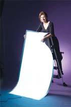
16 Solid State Lighting: OLED Large range of colours and design possible Flexible substrates Current Capabilities Target applications Full fabrication facility for light Strategic application: panels of size 10 cm x 10 cm on -light weight lighting source rigid substrate Future Expansion Urban application Fabrication facility for roll-to-roll - Lamps and decorative panels processing on flexible substrate - Furniture and building integrated lighting - Mood lighting Patent portfolio: 4 patents applied


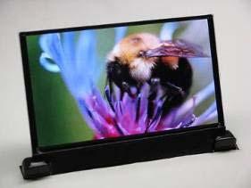
17 OLED DISPLAYS Prototype Display 1.5 inch diagonal, 128RGB x 128 Metal Lines COF Driver Display module, full color 96 (3) x 64, 1, passive matrix, consisting of the OLED display, COF and driver. Patent portfolio: 4 patents applied


18 Sensors Technology focus Sensor device design and fabrication Sensor arrays, multianalyte detection Application areas Healthcare, environmental, biomedical and food packaging, medical, process engineering, safety Temperature Gases Disease diagnostics Patent portfolio: 1 patent granted, 6 applications pending


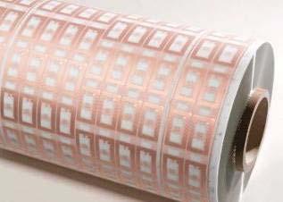
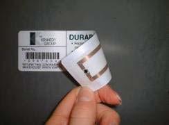
19 Low cost, printable electronics based tags Tags with printed electronic circuits for brand protection Smart tags incorporating memory and sensors Target Applications Passive Tag Brand protection Tracking for goods Excise controls Patent portfolio: 3 patents applied 16-bit memory label


20 Organic Photovoltaic Sub-modules Current capability On Glass Substrate Sub-modules of size 10 cm x 10 cm On Steel Substrate Small area device 3 mm x 3 mm Working towards Sub-modules on steel substrate Sub-modules on paper & PET substrate High throughput printing process Target applications Light weight power generation source Portable solar PV device on flexible substrate Patent portfolio: 7 patents applied
21 Summary FlexE Centre, IIT Kanpur is seeking academic and industry partners to further advance the frontiers of research in large area flexible electronics
The Future for Printed Electronics
 The Future for Printed Electronics Jon Helliwell National Centre for Printable Electronics 24 October, 2013 Copyright CPI 2013. All rights reserved What is Printed Electronics? Organic and printed electronics
Accelerating Scale Up of Large Area Electronics
 Accelerating Scale Up of Large Area Electronics Duncan Lindsay Business Development Director, CPI 2015 Centre for Process Innovation Limited. All Rights Reserved. Who are CPI? CPI is a UK technology innovation
Analysis of Wet Coating Thickness Effect on Transparent Conductive Electrode Performance using Silver Nanowire
 Analysis of Wet Coating Thickness Effect on Transparent Conductive Electrode Performance using Silver Nanowire 2017. 04. 25 Seung-Hyun Lee, PhD Senior Researcher Dept. Printed Electronics Korea Institute
Printable Electronics
 Printable Electronics Printable Electronics The Centre for Process Innovation From innovation to commercialisation The Centre for Process Innovation From innovation to commercialisation The High Value
Holst Centre Wireless Autonomous Sensor Technologies & Flexible Electronics
 February 10, 2011 Holst Centre Wireless Autonomous Sensor Technologies & Flexible Electronics Presentation overview -General overview -Research focus < 4 Holst Centre: a solid partner in research Independent,
Printed Electronics - Quo Vadis? What is Printed Electronics et Quo Vadis?
 Printed Electronics - Quo Vadis? Emil J.W. List Institute of Solid State Physics Graz University of Technology NanoTecCenter Weiz Forschungsgesellschaft mbh Agenda Introduction Motivation What is Printed
shaping global nanofuture ULTRA-PRECISE PRINTING OF NANOMATERIALS
 shaping global nanofuture ULTRA-PRECISE PRINTING OF NANOMATERIALS WHO ARE WE? XTPL S.A. is a company operating in the nanotechnology segment. The interdisciplinary team of XTPL develops on a global scale
Printable, Novel CNT Inks with V2V Technology
 Printable, Novel CNT Inks with V2V Technology William J. Hurley, Jr., PhD Chasm Technologies, Inc. Canton, MA June 23, 2010 New England Nanomanufacturing Summit 1 Outline CHASM Overview Alliance with SWeNT
Advancing Consumer Packaging Through Printable Electronics
 IPST Executive Conference, Atlanta, GA March 9-10, 2011 Advancing Consumer Packaging Through Printable Electronics Bernard Kippelen Professor, School of Electrical and Computer Engineering Director, Center
Printed Electronics: success stories and future commercial applications
 Printed Electronics: success stories and future commercial applications Dr Guillaume Chansin @gchansin June 2017 Helping you profit from emerging technologies Advantages of printed electronics Mass production
PILOT LINE FOR LARGE-AREA PRINTING OF ELECTRONIC AND PHOTONIC DEVICES. Simon Perraud, Ph.D. Vice president for European affairs
 PILOT LINE FOR LARGE-AREA PRINTING OF ELECTRONIC AND PHOTONIC DEVICES Simon Perraud, Ph.D. Vice president for European affairs ABOUT LITEN Liten is the research institute of CEA devoted to clean energy
 Organic and flexible Electronics in Saxony www.invest-in-saxony.com WElCOME Organic electronics are based on the discovery that specific organic materials possess semiconducting properties. Functional
Large Area, Flexible Electronics TWG. Chair: Dan Gamota, Jabil
 Large Area, Flexible Electronics TWG Chair: Dan Gamota, Jabil Large Area Flexible Electronics Roadmap History 09/2005 inemi Stakeholders identify Flexible Electronics as Future Growth Market and authorize
Herzlich willkommen. Druckbare Sensoren für Food Packaging ICT-Agri-Food Symposium. Sören Fricke Section Head Large Area & Flexible Systems
 Herzlich willkommen Druckbare Sensoren für Food Packaging ICT-Agri-Food Symposium Sören Fricke Section Head Large Area & Flexible Systems Agroscope Tänikon, 05.09.2017 Motivation Printed Sensors can be
Flexible Electronics: Revolutionary Products and Career Opportunities for Creative Engineers
 Flexible Electronics: Revolutionary Products and Career Opportunities for Creative Engineers TAPPI - PIMA Student Summit 2011 Michael Ciesinski President January 15, 2011 Microelectronics changed the world
Printing versus coating technology Which way Printed Electronics with solution coating will go?
 Printing versus coating technology Which way Printed Electronics with solution coating will go? Frank Schäfer, Andrea Glawe, Dr. Daniel Eggerath, KROENERT GmbH& Co KG, Schuetzenstrasse 105, 22761 Hamburg
Heterogeneous integration of autonomous smart films based on electrochromic transistors
 of autonomous smart films NEWSLETTER #5 www.smartwww.smart-ec.eu Objectives SMART-EC has finalized last August 2014; it aimed at the development of self-powered electrochromic (EC) display device with
ORGANIC ELECTRONICS: PHOTOLITHOGRAPHY OR PRINTING. Giles Lloyd Flex Europe Conference, 25th October 2016
 ORGANIC ELECTRONICS: PHOTOLITHOGRAPHY OR PRINTING Giles Lloyd Flex Europe Conference, 25th October 2016 Organic Electronics: Photoligthography or Printing? Lithography Printing Enabling flexible TFT sheet-fed
Nanotechnology, the infrastructure, and IBM s research projects
 Nanotechnology, the infrastructure, and IBM s research projects Dr. Paul Seidler Coordinator Nanotechnology Center, IBM Research - Zurich Nanotechnology is the understanding and control of matter at dimensions
PRINTED ELECTRONICS 3
 PRINTED ELECTRONICS 3 4 INKTEC PRINTED ELECTRONICS 5 6 INKTEC PRINTED ELECTRONICS 7 InkTec Leads New Paradigm in Printed Electronic Materials Applications OTFT, Memory Cell, Display, RFID and so on Product
RIT. Printing. Project Goals. Printing Radio Frequency Identification (RFID) Tag Antennas Using Inks Containing Metal Nanoparticles
 Tag Antennas Using Inks Containing Metal Nanoparticles") Printing Radio Frequency Identification (RFID) Tag Antennas Using Inks Containing Metal Nanoparticles Bruce E. Kahn Rochester Institute of Technology bkahn@mail.rit.edu http://www.rit.edu/~bekpph/ RIT
Printing Radio Frequency Identification (RFID) Tag Antennas Using Inks Containing Metal Nanoparticles Bruce E. Kahn Rochester Institute of Technology bkahn@mail.rit.edu http://www.rit.edu/~bekpph/ RIT
IMI Labs Semiconductor Applications. June 20, 2016
 IMI Labs Semiconductor Applications June 20, 2016 Materials Are At the Core of Innovation in the 21st Century Weight Space Flexibility Heat Management Lightweight Energy Efficient Temperature Energy Efficient
New Horizons. A new paradigm. of collaborative research
 New Horizons A new paradigm of collaborative research One of the immediate and complex challenges facing industry, business and government in Australia today is a need to increase exports, foreign investment
Emerging Print Technologies & Applications
 Emerging Print Technologies & Applications By: Pivotal Resources USA, Inc. 2901 Richmond Road #353 Lexington, KY 40509 (859) 230-0093 2013 PRIMIR/NPES EMERGING PRINT TECHNOLOGIES & APPLICATIONS TABLE OF
Flexible glass substrates for roll-to-roll manufacturing
 Science & Technology Flexible glass substrates for roll-to-roll manufacturing Corning - S. Garner, G. Merz, J. Tosch, C. Chang, D. Marshall, X. Li, J. Matusick, J. Lin, C. Kuo, S. Lewis, C. Kang ITRI -
MEMS in ECE at CMU. Gary K. Fedder
 MEMS in ECE at CMU Gary K. Fedder Department of Electrical and Computer Engineering and The Robotics Institute Carnegie Mellon University Pittsburgh, PA 15213-3890 fedder@ece.cmu.edu http://www.ece.cmu.edu/~mems
OVERVIEW OF PLASTIC SUBSTRATES FOR PRINTED ELECTRONICS
 OVERVIEW OF PLASTIC SUBSTRATES FOR PRINTED ELECTRONICS Robert Rus:n Sr. Applica+on and Market Development Manager Special thanks to: Karl Rakos Bill MacDonald Melinex polyester film Mylar polyester film
Printing as a material deposition process
 Printing as a material deposition process Printing Materials, Mumbai 5 th March 2011 Prof. Fritz Bircher, www.printtechnology.ch 1 Presentation outline Material deposition The inkjet printing process Interaction
Plastic Electronics Market Development. by Mr. Ed van den Kieboom Executive Board Member Plastic Electronics Foundation
 Plastic Electronics Market Development by Mr. Ed van den Kieboom Executive Board Member Plastic Electronics Foundation Plastic Electronics Foundation Established April 2005 Private non profit organization
Low Temperature Integration of Thin Films and Devices for Flexible and Stretchable Electronics
 Low Temperature Integration of Thin Films and Devices for Flexible and Stretchable Electronics Pooran Joshi, Stephen Killough, and Teja Kuruganti Oak Ridge National Laboratory FIIW 2015 Displays and PV
Making a Material Difference
 Making a Material Difference Founded as a QinetiQ corporate investment in January 2002 Spun out in 2007 Locations: Rochester, NYS, USA (HQ and Production) Farnborough and Malvern, UK (R&D, Production and
Micro-PackS, Technology Platform. Security Characterization Lab Opening
 September, 30 th 2008 Micro-PackS, Technology Platform Security Characterization Lab Opening Members : Micro-PackS in SCS cluster From Silicium to innovative & commucating device R&D structure, gathering
NanoFabrication Kingston. Seminar and Webinar January 31, 2017 Rob Knobel Associate Professor, Dept. of Physics Queen s University
 NanoFabrication Kingston Seminar and Webinar January 31, 2017 Rob Knobel Associate Professor, Dept. of Physics Queen s University What is NFK? It s a place, an team of experts and a service. The goal of
The Centre for Process Innovation
 The Centre for Process Innovation The Centre for Process Innovation From innovation to commercialisation The future inspired... The High Value Manufacturing Catapult is a partnership between industry and
Printed and Hybrid Integration
 Printed and Hybrid Integration Neil Chilton PhD Technical Director, Printed Electronics Limited, UK Neil.Chilton@PrintedElectronics.com Printed Electronics Limited (PEL) General Overview PEL was founded
Printed Electronics. Applications
 Printed Electronics Research Through University-Industry Partnerships Outline Background on Printed Electronics (PE) Corporate Partnerships Raytheon UMass Lowell Research Institute (RURI) Printed Electronics
Plan Optik AG. Plan Optik AG PRODUCT CATALOGUE
 Plan Optik AG Plan Optik AG PRODUCT CATALOGUE 2 In order to service the high demand of wafers more quickly, Plan Optik provides off the shelf products in sizes from 2 up to 300mm diameter. Therefore Plan
DuPont Reflections on Photovoltaics
 DuPont Reflections on Photovoltaics Steven C. Freilich Technology Director E. I. du Pont de Nemours and Co. CTO Electronics and Communication April 23, 2009 The Vision of DuPont 2 To be the world s most
Consortium Capabilities
 Consortium Capabilities The driver in advanced materials development is to create products with competitive advantages. Products must continuously become faster, lighter and cheaper and must provide additional
Complementary Organic Semiconductor and Metal Integrated Circuits
 Complementary Organic Semiconductor and Metal Integrated Circuits COSMIC will generate an organic CMOS technology platform from design to manufacturing level. COSMIC will produce highly complex lead applications
Des MEMS aux NEMS : évolution des technologies et des concepts aux travers des développements menés au LETI
 Des MEMS aux NEMS : évolution des technologies et des concepts aux travers des développements menés au LETI Ph. Robert 1 Content LETI at a glance From MEMS to NEMS: 30 years of technological evolution
Henkel solutions enabling printed electronics. Dr. Crystal Yang
 Henkel solutions enabling printed electronics Dr. Crystal Yang Agenda 1. Introduction Henkel 2. Trends in Printed Electronics 3. Novel materials enabling Printed Electronics New high speed printable silver
MICROFLEX Project: MEMS on New Emerging Smart Textiles/Flexibles
 MICROFLEX Project: MEMS on New Emerging Smart Textiles/Flexibles S Beeby, M J Tudor, R Torah, K Yang, Y Wei Dr Steve Beeby ESD Research Group Smart Fabrics 2011 5 th April 2011 Overview Introduce the MicroFlex
GLOBAL MARKETS, TECHNOLOGIES AND MATERIALS FOR THIN AND ULTRATHIN FILMS
 GLOBAL MARKETS, TECHNOLOGIES AND MATERIALS FOR THIN AND ULTRATHIN FILMS SMC057C August Margareth Gagliardi Project Analyst ISBN: 1-62296-338-5 BCC Research 49 Walnut Park, Building 2 Wellesley, MA 02481
COMPANY PRESENTATION
 COMPANY PRESENTATION Unrivalled know-how at the service of our clients Can one be passionate about PET film? We at Coveme believe so, because this is simply what 40 years of engineering polyester has taught
We give vision to all surfaces Plastic Electronics Dresden.
 We give vision to all surfaces Plastic Electronics Dresden www.isorg.fr laurent.jamet@isorg.fr 1 When Printed Electronics meet Design, Usages and Brands for eye catching and appealing products Company
Synthesis of Silicon. applications. Nanowires Team. Régis Rogel (Ass.Pr), Anne-Claire Salaün (Ass. Pr)
, Anne-Claire Salaün (Ass. Pr)") Synthesis of Silicon nanowires for sensor applications Anne-Claire Salaün Nanowires Team Laurent Pichon (Pr), Régis Rogel (Ass.Pr), Anne-Claire Salaün (Ass. Pr) Ph-D positions: Fouad Demami, Liang Ni,
Synthesis of Silicon nanowires for sensor applications Anne-Claire Salaün Nanowires Team Laurent Pichon (Pr), Régis Rogel (Ass.Pr), Anne-Claire Salaün (Ass. Pr) Ph-D positions: Fouad Demami, Liang Ni,
MID Manufacturing Process.
 3D Aerosol Jet Printing An Emerging MID Manufacturing Process. Dr. Martin Hedges Neotech Services MTP, Nuremberg, Germany info@neotechservices.com Aerosol Jet Printing Aerosol Jet Process Overview Current
Mass transfer with elastomer stamps for microled displays.
 Frontiers in Assembly Mass transfer with elastomer stamps for microled displays. Matt Meitl X-Celeprint, Inc. mmeitl@x-celeprint.com 1 The best materials for the best displays The materials identify the
For personal use only
 For personal use only 7 JUNE 2017 ASX MEDIA RELEASE Nanocube Memory Ink Development Progress Strategic Elements Ltd (ASX : SOR) is pleased to provide an update on the Nanocube Memory ink invented by the
EMERGING INKJET PRINTING TECHNOLOGIES, APPLICATIONS AND GLOBAL MARKETS
 EMERGING INKJET PRINTING TECHNOLOGIES, APPLICATIONS AND GLOBAL MARKETS AVM091B November 2014 Andrew McWilliams Project Analyst ISBN: 1-56965-999-0 BCC Research 49 Walnut Park, Building 2 Wellesley, MA
A New Paradigm for Disruptive Technology Development and Transition
 A New Paradigm for Disruptive Technology Development and Transition Gregory B. Raupp, Director Flexible Display Center at Arizona State University ASU Research Park Tempe, Arizona 85224 raupp@asu.edu http://flexdisplay.asu.edu
EU Research project proposals (call for Finnish companies)
") EU Research project proposals (call for Finnish companies) 11th EEMELI Workshop 29 th August 2012 Jukka Hast Research Professor VTT Technical Research Centre of Finland 04/10/2012 2 General ICT theme work
EU Research project proposals (call for Finnish companies) 11th EEMELI Workshop 29 th August 2012 Jukka Hast Research Professor VTT Technical Research Centre of Finland 04/10/2012 2 General ICT theme work
Pattern Coating by Slot-Die SCOTT A. ZWIERLEIN FRONTIER INDUSTRIAL TECHNOLOGY, INC. AIMCAL FALL TECHNICAL CONFERENCE 2013
 Pattern Coating by Slot-Die SCOTT A. ZWIERLEIN FRONTIER INDUSTRIAL TECHNOLOGY, INC. AIMCAL FALL TECHNICAL CONFERENCE 2013 Program: Slot-Die Coating Overview Industries for slot-die coating Stripe coating
Technology Transfer at CERN
 Technology Transfer at CERN Enrico Chesta Head of CERN Technology Transfer and Intellectual Property Management Section Knowledge Transfer Group, FP Department How can CERN have an impact beyond fundamental
Research Centers. MTL ANNUAL RESEARCH REPORT 2016 Research Centers 147
 Research Centers Center for Integrated Circuits and Systems... 149 MIT/MTL Center for Graphene Devices and 2D Systems... 150 MIT/MTL Gallium Nitride (GaN) Energy Initiative... 151 The MIT Medical Electronic
Processes for Flexible Electronic Systems
 Processes for Flexible Electronic Systems Michael Feil Fraunhofer Institut feil@izm-m.fraunhofer.de Outline Introduction Single sheet versus reel-to-reel (R2R) Substrate materials R2R printing processes
Linking Smart Specialization with Technology Transfer in Science and Technology Park Planning
 Linking Smart Specialization with Technology Transfer in Science and Technology Park Planning EU4Innovation: Fostering Research-Industry Links 1 st October 2018, Tbilisi Mr. Nikos Giannoulidis Director
Passion for Performance.
 HANNECARD Passion for Performance. When it comes to a printing job, the options are few : the printing quality needs to be outstanding, costs as low as possible and short turnaround times. Whatever printing
ENERGY SCIENCES INC. EB COATING DEVELOPMENTS FOR GRAPHIC ARTS
 ENERGY SCIENCES INC. EB COATING DEVELOPMENTS FOR GRAPHIC ARTS WHAT IS EB? INNOVATIVE METHOD OF IMMEDIATELY DRYING INKS COATINGS ADHESIVES WITHOUT HEAT OR LIGHT. HOW DOES AN E-BEAM WORK? Ø FILAMENTS EMIT
AC : EXPERIMENTAL MODULES INTRODUCING MICRO- FABRICATION UTILIZING A MULTIDISCIPLINARY APPROACH
 AC 2011-1595: EXPERIMENTAL MODULES INTRODUCING MICRO- FABRICATION UTILIZING A MULTIDISCIPLINARY APPROACH Shawn Wagoner, Binghamton University Director, Nanofabrication Labatory at Binghamton University,
Additive & Inkjet Printing Technologies & Applications
 Additive & Inkjet Printing Technologies & Applications Debbie Thorp, Business Development Director Global Inkjet Systems Ltd Silverstone Park - October 2018 GIS Products DFE Atlas User Interface Machine
EU's contribution to research and innovation in Electronics
 EU's contribution to research and innovation in Electronics Henri.RAJBENBACH@ec.europa.eu Nikolaos.KYRLOGLOU@ec.europa.eu European Commission DG CONNECT (not legally binding presentation) SEMICON Europa-Flex
Ubiquitous Displays and Sensors Activating Surfaces with Flexible Electronics. Dean Baker, Director FlexEnable. APAC Innovation Summit 2016, Hong Kong
 Ubiquitous Displays and Sensors Activating Surfaces with Flexible Electronics Dean Baker, Director FlexEnable, Hong Kong Activating surfaces with flexible displays and sensors Flexible Plastic Displays
DTU DANCHIP an open access micro/nanofabrication facility bridging academic research and small scale production
 DTU DANCHIP an open access micro/nanofabrication facility bridging academic research and small scale production DTU Danchip National Center for Micro- and Nanofabrication DTU Danchip DTU Danchip is Denmark
KIC EIT Raw Materials
 KIC EIT Raw Materials Text Text Dr. Lisa Maria T. O Donoghue Dublin 18.10.17 Picture source http://www.falconautoonline.com/incoming-material/ What is a EIT-KIC KIC (acronym of Knowledge Innovation Community)
Flexible Glass Applications & Process Scaling
 Flexible Glass Applications & Process Scaling Sean Garner, Sue Lewis, Gary Merz, Alex Cuno, Ilia Nikulin October 16, 2017 Outline Flexible Glass Applications Process Scaling Summary 2 Flexible Glass Enables
For personal use only
 Pooled Development Fund funding Australian SME owned projects in technology and resources. Specialty focus on backing projects with large scale upside potential. Maintain significant control over direction
Scientific Highlights 2016
 Scientific Highlights 2016 Science and Technology Sector Schools and Faculties Faculty of Science Louvain School of Engineering (EPL) Faculty of Architecture, Architectural Engineering and Urban Planning
Wearable Robotics Funding Opportunities and Commercialization of Robotics and Mobility Systems Bruce Floersheim, Ph.D., P.E.
 Wearable Robotics Funding Opportunities and Commercialization of Robotics and Mobility Systems Bruce Floersheim, Ph.D., P.E. www.wearablerobotics.com Help shape a global future leveraging technology in
Здра вствуйте, това рищи!
 Manufacturing of Smart Objects by Printing Technologies Здра вствуйте, това рищи! Moscow / RUS, June 05, 2013 Reinhard R. Baumann Chemnitz University of Technology Chair of Digital Printing Fraunhofer
Figure 7 Dynamic range expansion of Shack- Hartmann sensor using a spatial-light modulator
 Figure 4 Advantage of having smaller focal spot on CCD with super-fine pixels: Larger focal point compromises the sensitivity, spatial resolution, and accuracy. Figure 1 Typical microlens array for Shack-Hartmann
Design and Innovation Centre. Banaras Hindu University and Indian Institute of Technology (BHU) Varanasi , UP, INDIA
 Varanasi , UP, INDIA") Design and Innovation Centre at and Indian Institute of Technology (BHU) Varanasi 221005, UP, INDIA with Spokes Mahatma Gandhi Kashi Vidyapeeth (MGKVP), Varanasi (State University) Indian Institute of
Design and Innovation Centre at and Indian Institute of Technology (BHU) Varanasi 221005, UP, INDIA with Spokes Mahatma Gandhi Kashi Vidyapeeth (MGKVP), Varanasi (State University) Indian Institute of
IBM Research - Zurich Research Laboratory
 October 28, 2010 IBM Research - Zurich Research Laboratory Walter Riess Science & Technology Department IBM Research - Zurich wri@zurich.ibm.com Outline IBM Research IBM Research Zurich Science & Technology
Surrey Knowledge Transfer Account
 Surrey Knowledge Transfer Account Innovation Powered. Innovation Powered Innovation is vital if the UK is to remain competitive on the world stage. The University of Surrey has a track record of successful
Printed Organic Transistors for Ultraflexible and Stretchable Electronics
 2011/6/2 20:00-22:00 Lake Buena Vista, Florida USA CPMT Seminar Printed Devices and Large Area Interconnect Technologies for New Electronics Printed Organic Transistors for Ultraflexible and Stretchable
Projects and Partners Working with Chalcogenide Advanced Manufacturing Partnership (ChAMP)
") Projects and Partners Working with Chalcogenide Advanced Manufacturing Partnership (ChAMP) Dr John Lincoln Industrial Liaison Officer j.lincoln@soton.ac.uk March 2015 ChAMP Aims Establish world leading
Projects and Partners Working with Chalcogenide Advanced Manufacturing Partnership (ChAMP) Dr John Lincoln Industrial Liaison Officer j.lincoln@soton.ac.uk March 2015 ChAMP Aims Establish world leading
The role of university science parks in business-university research collaboration
 The role of university science parks in business-university research collaboration The Dowling Review: enhancing business-university research collaboration Dr Malcolm Parry OBE, Director and CEO The Surrey
Outstanding performance starts with the selection of your masterbatch partner. Your expert in masterbatches and compounds. sukano.
 Driven by expertise Outstanding performance starts with the selection of your masterbatch partner Your expert in masterbatches and compounds Sukano is a world leader in the development and production of
Supplementary Information
 Supplementary Information Wireless thin film transistor based on micro magnetic induction coupling antenna Byoung Ok Jun 1, Gwang Jun Lee 1, Jong Gu Kang 1,2, Seung Uk Kim 1, Ji Woong Choi 1, Seung Nam
NextFlex: Enabling a Domestic Manufacturing Ecosystem for Flexible Hybrid Electronics (Extended Abstract)
") NextFlex: Enabling a Domestic Manufacturing Ecosystem for Flexible Hybrid Electronics (Extended Abstract) Benjamin J. Leever*, Eric W. Forsythe + *Air Force Research Laboratory, 2179 12th St., B652/R122,
NextFlex: Enabling a Domestic Manufacturing Ecosystem for Flexible Hybrid Electronics (Extended Abstract) Benjamin J. Leever*, Eric W. Forsythe + *Air Force Research Laboratory, 2179 12th St., B652/R122,
MEDIA RELEASE FOR IMMEDIATE RELEASE 26 JULY 2016
 MEDIA RELEASE FOR IMMEDIATE RELEASE 26 JULY 2016 A*STAR S IME KICKS OFF CONSORTIA TO DEVELOP ADVANCED PACKAGING SOLUTIONS FOR NEXT-GENERATION INTERNET OF THINGS APPLICATIONS AND HIGH-PERFORMANCE WIRELESS
(12) Patent Application Publication (10) Pub. No.: US 2006/ A1
 Patent Application Publication (10) Pub. No.: US 2006/ A1") (19) United States US 2006O1993 13A1 (12) Patent Application Publication (10) Pub. No.: US 2006/01993 13 A1 Harting et al. (43) Pub. Date: Sep. 7, 2006 (54) THIN FILM SEMICONDUCTOR DEVICE AND METHOD OF
(19) United States US 2006O1993 13A1 (12) Patent Application Publication (10) Pub. No.: US 2006/01993 13 A1 Harting et al. (43) Pub. Date: Sep. 7, 2006 (54) THIN FILM SEMICONDUCTOR DEVICE AND METHOD OF
Printed Electronics Product Types & Markets. Vince Cahill, VCE Solutions
 Printed Electronics Product Types & Markets Vince Cahill, VCE Solutions Printed Electronic Product Types Printed circuits boards Printed logic / memory Printed batteries Membrane switches Photovoltaics
THE BIOMEDICAL ENGINEERING TEACHING & INNOVATION CENTER. at Boston University s College of Engineering
 THE BIOMEDICAL ENGINEERING TEACHING & INNOVATION CENTER at Boston University s College of Engineering The vision At Boston University s College of Engineering, we intend to create an exciting new resource
HipoCIGS: enamelled steel as substrate for thin film solar cells
 HipoCIGS: enamelled steel as substrate for thin film solar cells Lecturer D. Jacobs*, Author S. Efimenko, Co-author C. Schlegel *:PRINCE Belgium bvba, Pathoekeweg 116, 8000 Brugge, Belgium, djacobs@princecorp.com
Printing Beyond Color. Printed Smart Objects on Advanced Paper Substrates. Reinhard R. Baumann
 Printing Beyond Color Printed Smart Objects on Advanced Paper Substrates June 17, 2009 member of Reinhard R. Baumann member of Chemnitz University of Technology Institute for Print and Media Technology
Research Strategy of Tampere University Community
 Research Strategy of Tampere University Community Tampere university community is made up of the research-intensive Tampere University and development-focused Tampere University of Applied Sciences. These
Short Course on Flexible Electronics Schedule
 DAY 1: Monday, 3 rd July, 2017 (Venue: Morning Session L-16, Afternoon Session L-14, Mixer-Ashiana) 8:30 9:00 Registration: outside L-16 at ground level Monica Katiyar : Introduction to Short Course on
UVISEL. Spectroscopic Phase Modulated Ellipsometer. The Ideal Tool for Thin Film and Material Characterization
 UVISEL Spectroscopic Phase Modulated Ellipsometer The Ideal Tool for Thin Film and Material Characterization High Precision Research Spectroscopic Ellipsometer The UVISEL ellipsometer offers the best combination
Emerging MEMS & Sensor Technologies to Watch: Alissa M. Fitzgerald, Ph.D., Founder & CEO Semicon West 2018
 Emerging MEMS & Sensor Technologies to Watch: 2018 Alissa M. Fitzgerald, Ph.D., Founder & CEO amf@amfitzgerald.com Outline About AMFitzgerald What emerging means in this presentation Emerging MEMS & sensor
IROST Programmes and Activities
 Iranian Research Organization for Science and Technology )IROST) IROST Programmes and Activities 2016-2017 Prepared by: Dr. Mahmoud Molanejad Acting President for International Cooperation and Fatemeh
Japan Barrier Society
 ISO/TC61/SC11/WG3 Pre NWIP Japan Barrier Society Agenda Background - Features and market trend of flexible electronics devices - High-barrier film as substrate of flexible electronics devices Conventional
Put your best ideas forward.
 Improve the way people view your brand. High-performance optical polymers and films for the electronics market Put your best ideas forward. The world is increasingly connected by technology that uses electronic
Accelerating Collective Innovation: Investing in the Innovation Landscape
 PCB Executive Forum Accelerating Collective Innovation: Investing in the Innovation Landscape How a Major Player Uses Internal Venture Program to Accelerate Small Players with Big Ideas Dr. Joan K. Vrtis
Top 50 Emerging Technologies & Growth Opportunities
 Top 50 Emerging Technologies & Growth Opportunities Multi-billion Dollar Technologies Ready to Energize Industries and Transform our World THE VALUE PROPOSITION TechVision s annual Top 50 Emerging Technologies
CASE STUDY: MODULAR BLIND COLLABORATIVE DESIGN AND PRINTING USING THE CREATIF SOFTWARE SUITE AND FUTURE PERSPECTIVES
 CASE STUDY: MODULAR BLIND COLLABORATIVE DESIGN AND PRINTING USING THE CREATIF SOFTWARE SUITE AND FUTURE PERSPECTIVES Partners involved and contact details: Diffus Design: Hanne-Louise Johannesen: hanne-louise@diffus.dk
REINVENTING PACKAGING PRODUCTION EBOOK BY ASAHI PHOTOPRODUCTS
 REINVENTING PACKAGING PRODUCTION EBOOK BY ASAHI PHOTOPRODUCTS ABOUT ASAHI PHOTOPRODUCTS THE GOAL OF THIS EBOOK For consumer product companies, the quality and consistency of packaging is critical to ensuring
PROJECT FINAL REPORT
 PROJECT FINAL REPORT Grant Agreement number: 247978 Project acronym: POLARIC Project title: Printable, organic and large-area realisation of integrated circuits Funding Scheme: CP Period covered: from
Innovative Vacuum Solutions
 100.131.02 Innovative Vacuum Solutions for Flat Panel Display Vacuum Solutions for DRYVAC SYSTEMS THE LEYBOLD STANDARD for Flat Panel Display With our DRYVAC SYSTEM platform we offer innovative solutions