UVISEL. Spectroscopic Phase Modulated Ellipsometer. The Ideal Tool for Thin Film and Material Characterization
|
|
|
- Corey Bond
- 5 years ago
- Views:
Transcription


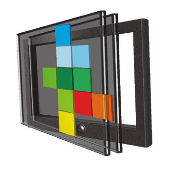

1 UVISEL Spectroscopic Phase Modulated Ellipsometer The Ideal Tool for Thin Film and Material Characterization


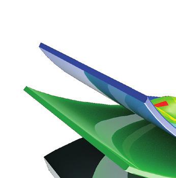
2 High Precision Research Spectroscopic Ellipsometer The UVISEL ellipsometer offers the best combination of flexibility and performance for thin film characterization. Precision Built on 25 years of experience, the UVISEL phase modulated ellipsometer delivers high precision and high resolution measurements, with the best signal to noise ratio, ideal for research on nano and micro scale structures. The UVISEL delivers long-term, stable measurements without the need for regular calibration. Wide Spectral Range We offer several UVISEL configurations capable of covering a wide spectral range from nm. The use of monochromators enables the selection of the spectral range and resolution that best suits your measurement needs. Flexibility Powerful Software The UVISEL ellipsometer offers a flexible design, enabling the best fit to your application needs. Manual or automatic goniometer, sample stage and microspot optics Large variety of accessories Ex-situ, in-situ and cost-effective configurations available The DeltaPsi 2 ellipsometry software presents an intuitive interface for instrument control, measurement and data processing. The largest variety of data acquisition and modeling functions gives research engineers the full performance of ellipsometric analysis. A simple interface allows the operator to perform routine tasks very easily.


 for real-time control of thin film deposition or etching processes.")


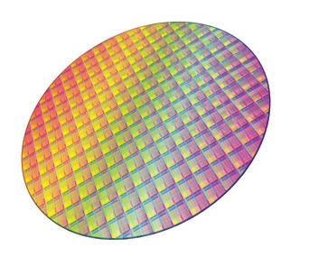
3 Film Thickness Optical Constants Roughness and Interface Material Properties UVISEL Ex-Situ The UVISEL Ex-Situ is available in four different spectral ranges from FUV to NIR. A large array of options and accessories offers enhanced performance and versatility. Options & Accessories Motorized XY stage Rotation stage Temperature controlled stage Automatic goniometer Reflectometry module Electrochemical cell Liquid cell Sealed cell UVISEL In-Situ The UVISEL In-Situ can be easily mounted onto process chambers (PECVD, MOCVD, sputter, evaporation, ALD, MBE) for real-time control of thin film deposition or etching processes. It provides real-time calculation of film thickness and optical constants. Using the adaptation kit, it is possible to easily switch between in-situ and ex-situ configurations and experiment with new applications. UVISEL mounted on a CVD chamber UVISEL LT The UVISEL LT is a cost-effective configuration featuring a compact, integrated goniometer with no compromise on data quality. The setting of the goniometer angle can be selected to best fit with your applications. The stage can accommodate samples up to 200 mm in size, with substrate thickness up to 17 mm. UVISEL In-Line For the demanding needs of flexible electronic devices, flexible displays and flexible solar panels, the UVISEL In-Line is fully compatible with roll-to-roll processing. The use of our patented multiwavelength detection system allows for a very fast acquisition time for superior thin film uniformity control of the moving substrate. The UVISEL Series is Based on Phase Modulation Technology. Specific features of this technology are: No moving parts during signal acquisition High modulation frequency (50 khz) Ψ (0-90) and (0-360) angles are measured over their entire range


 fitting Integrated interface for")
 and reporting.")
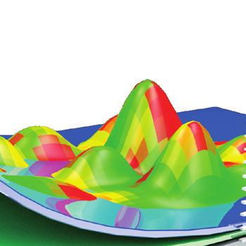
4 Powerful DeltaPsi2 Software from Research to Routine Our ellipsometers are driven by the powerful and advanced DeltaPsi2 software, designed for accurate and flexible measurement and characterization of thin film structures. The DeltaPsi2 software offers complete functionality for measurements, modeling and reporting, in addition to automatic operations, which facilitate routine thin film analysis. Measurement Reflection and transmission ellipsometry Reflectance and transmittance intensity Kinetic ellipsometry Variable angle Depolarization Scatterometry Mueller matrix Modeling & Simulation Large materials library based on reference database and dispersion relations Roughness or interface (EMA) Alloy composition, crystallinity Periodic structure Graded optical constants Anisotropic structures, uniaxial and biaxial films Periodic structure Nanoparticle modeling Automatic backside correction for transparent substrates Bandgap calculations (n,k) fitting Integrated interface for measurement, analysis and reporting with drag and drop operations Customizable data reporting Data Reporting Customized reporting 2D/3D image display Data import/export package Automatic Operations Recipes provide full automation of measurement, analysis, mapping (if selected) and reporting. The recipe contains all of the settings for the sample under analysis and is launched in one click. Data reprocessing Statistical analysis Recipe results with a 3D view of a sample map Measurements performed with a motorized XY stage
, as")


5 The Power of Ellipsometry for Thin Films and Nanostructures Obtain thin film thickness and optical constants (n,k), as well as other properties of your thin film structure, including surface roughness, composition, and band gap. Semiconductors Flat Panel Displays Optoelectronics Photovoltaics Optical and Functional Coatings Surface Chemistry and Biotechnology LED Application Organic Photovoltaics 22% GaN + 78% void 248 Å 58% GaN + 42% void 149 Å 90% GaN + 10% void 128 Å GaN 8001 Å GaN Thickness and Roughness PEDOT:PSS ITO Gradient 441 Å 1539 Å PEDOT:PSS Thickness Sapphire substrate Glass substrate The µm Gallium Nitride exhibits a strong roughness, described by a mixture of GaN and void using the Effective Medium Approximation. The fit was performed over the full measurement range from 0.6 to 6.5 ev with an excellent χ 2 parameter. The ITO layer is modeled with a linear gradient. Flexible Electronics Over Coat 92% Over Coat + Ag nw 8% 782 Å Plastic foil Ag Nanowires Modeling The UVISEL was used to measure the plastic foil over the wavelength range nm. The goal is to characterize the inclusion of nanowires into the dielectric matrix: percentage, shape and orientation.
1 69 74 72 00 USA: Tel: +1 732 494 8660 Japan: Tel: +81-(0)3 6206 4721")
1 69 74 72 00 www.horiba.com/scientific info.sci@horiba.")


 and tilt Motorized stage")

6 Find out more at Contact Us France: Tel: +33 (0) USA: Tel: Japan: Tel: +81-(0) Germany: Tel: +49 (0) UK: Tel: +44 (0) China: Tel: +86 (0) Brazil: Tel: +55 (0) Other: Tel: +33 (0) Worldwide Training and Technical Support Our staff of experienced application and service engineers, located around the world, provides full support for your instrument. Well equipped application laboratories allow for sample analysis and hands-on training for new and experienced users. HORIBA Worldwide Follow Us UVISEL Specifications UVISEL UVISEL FUV UVISEL NIR UVISEL ER UVISEL LT Spectral Range nm nm nm nm nm nm Light Source 75 W Xenon lamp 150 W Xenon lamp 75 W Xenon lamp 150 W Xenon lamp 75 W Xenon lamp Microspot Manual microspot: 3 positions: mm Automatic microspot option: 4 positions: mm Spot diameter: 3 mm Sample Stage Manual stage: 150 mm, manually adjustable height (20 mm) and tilt Motorized stage option: 200 mm or 300 mm Rotation stage option: 150 mm, high precision automated sample rotation (360 - θ only), resolution: Goniometer Manual goniometer: manually adjustable angle from 55 to 90 by step of 5 Motorized goniometer option: automatically adjustable angle from 40 to 90 by step of 0.01 High resolution scanning monochromator Monochromator For FUV-VIS range: High sensitivity photomultiplier detectors For NIR extension: InGaAs detector This document is not contractually binding under any circumstances - Printed in France - HORIBA Jobin Yvon 11/2014
UVISEL 2. Interface. Thickness. Refractive index. Roughness. Extinction coefficient. Scientific Ellipsometric Platform
 Scientific Ellipsometric Platform The Ultimate Solution to Every Challenge in Thin Film Measurement Refractive index Interface Roughness Extinction coefficient Thickness Å to µm A Breakthrough in Thin
PhE102-VASE. PHE102 Variable Angle Spectroscopic Ellipsometer. Angstrom Advanced Inc. Angstrom Advanced. Angstrom Advanced
 Angstrom Advanced PhE102-VASE PHE102 Variable Angle Spectroscopic Ellipsometer Angstrom Advanced Instruments for Thin Film and Semiconductor Applications sales@angstromadvanced.com www.angstromadvanced.com
M J.A. Woollam Co., Inc. Ellipsometry Solutions
 M-2000 J.A. Woollam Co., Inc. Ellipsometry Solutions Speed Discover the Difference Focused M-2000 The M-2000 line of spectroscopic ellipsometers is engineered to meet the diverse demands of thin film characterization.
LITE /LAB /SCAN /INLINE:
 Metis Metis LITE /LAB /SCAN/ INLINE Metis LITE /LAB /SCAN /INLINE: Spectral Offline and Inline Measuring System, using Integrating Sphere, for coatings on foils/web and on large size glasses To ensure
Add CLUE to your SEM. High-efficiency CL signal-collection. Designed for your SEM and application. Maintains original SEM functionality
 Add CLUE to your SEM Designed for your SEM and application The CLUE family offers dedicated CL systems for imaging and spectroscopic analysis suitable for most SEMs. In addition, when combined with other
MICROSCOPIC THIN FILM METROLOGY AND VISUALIZATION
 MICROSCOPIC THIN FILM METROLOGY AND VISUALIZATION Hex. Boron Nitride on SiO 2 MoS 2 on Sapphire Protein Spots on Glass Graphene on SiO 2 (300 nm) Si PCBM on SiO 2 Graphene on Copper Solar cell on PET Transparent
A Laser-Based Thin-Film Growth Monitor
 TECHNOLOGY by Charles Taylor, Darryl Barlett, Eric Chason, and Jerry Floro A Laser-Based Thin-Film Growth Monitor The Multi-beam Optical Sensor (MOS) was developed jointly by k-space Associates (Ann Arbor,
Advanced Research Raman System Raman Spectroscopy Systems
 T600 Advanced Research Raman System Raman Spectroscopy Systems T600 Advanced Research Raman System T600 Triple stage Raman Spectrometer: The only solution for unprecedented stability and performance! Robust
NATIONAL INSTITUTE OF RESEARCH AND DEVELOPMENT FOR OPTOELECTRONICS
 SERVICES OFFER Measurements DESCRIPTION OF THE LAB The laboratory characterize by optical and complementary methods of the materials, components and systems with application in optoelectronics. The destination
Aqualog. Water Quality Measurements Made Easy PARTICLE CHARACTERIZATION ELEMENTAL ANALYSIS FLUORESCENCE
 Aqualog Water Quality Measurements Made Easy ELEMENTAL ANALYSIS FLUORESCENCE GRATINGS & OEM SPECTROMETERS OPTICAL COMPONENTS PARTICLE CHARACTERIZATION RAMAN SPECTROSCOPIC ELLIPSOMETRY SPR IMAGING Water
Thin film measurement solutions: Hardware, software, applications
 Thin film measurement solutions: Hardware, software, applications We develop and manufacture wide range of optical thin-film metrology instruments from high-precision sophisticated ellipsometry and reflectometry
Applications of Steady-state Multichannel Spectroscopy in the Visible and NIR Spectral Region
 Feature Article JY Division I nformation Optical Spectroscopy Applications of Steady-state Multichannel Spectroscopy in the Visible and NIR Spectral Region Raymond Pini, Salvatore Atzeni Abstract Multichannel
Microprobe-enabled Terahertz sensing applications
 Microprobe-enabled Terahertz sensing applications World of Photonics, Laser 2015, Munich Protemics GmbH Aachen, Germany Terahertz microprobing technology: Taking advantage of Terahertz range benefits without
Dual-FL. World's Fastest Fluorometer. Measure absorbance spectra and fluorescence simultaneously FLUORESCENCE
 Dual-FL World's Fastest Fluorometer Measure absorbance spectra and fluorescence simultaneously FLUORESCENCE 100 Times Faster Data Collection The only simultaneous absorbance and fluorescence system available
Your thin films visualized.
 Your thin films visualized. Graphene Graphene Protein spots on glass Graphene PCBM on SiO 2 SAM Solar cell on PET Transparent substrate Liquid/liquid interface SAM pattern PMMA film on Si-Wafer Monolayer
Aqualog. Water Quality Measurements Made Easy FLUORESCENCE
 Aqualog Water Quality Measurements Made Easy FLUORESCENCE Water quality measurements made easy The only simultaneous absorbance and fluorescence system for water quality analysis! The new Aqualog is the
GSM OPTICAL MONITORING FOR HIGH PRECISION THIN FILM DEPOSITION
 OPTICAL MONITORING FOR HIGH PRECISION THIN FILM DEPOSITION OPTICAL MONITORING TECHNOLOGIES ENABLING OUR NEW WORLD! - ACHIEVING MORE DEMANDING THIN FILM SPECIFICATIONS - DRIVING DOWN UNIT COSTS THE GSM1101
DeltaMyc. Fluorescence Lifetime Mapping Microscope. Affordable Fluorescence Lifetime Imaging Microscopy (FLIM)
") DeltaMyc Fluorescence Lifetime Mapping Microscope Affordable Fluorescence Lifetime Imaging Microscopy (FLIM) DeltaMyc Affordable Fluorescence Imaging Lifetime Microscopy (FLIM) At last, an affordable yet
DeltaMyc Fluorescence Lifetime Mapping Microscope Affordable Fluorescence Lifetime Imaging Microscopy (FLIM) DeltaMyc Affordable Fluorescence Imaging Lifetime Microscopy (FLIM) At last, an affordable yet
Inline Control of an Ultra Low-k ILD layer using Broadband Spectroscopic Ellipsometry
 Inline Control of an Ultra Low-k ILD layer using Broadband Spectroscopic Ellipsometry Ronny Haupt, Jiang Zhiming, Leander Haensel KLA-Tencor Corporation One Technology Drive, Milpitas 95035, CA Ulf Peter
Real Time Etching End Point Monitors (OES & Interferometer type)
") Real Time Etching End Point Monitors (OES & Interferometer type) HORIBA Semiconductor Products Softwares Applications Websites and download Products History of HORIBA End Point Monitor 1/2 26 years experience
Real Time Etching End Point Monitors (OES & Interferometer type) HORIBA Semiconductor Products Softwares Applications Websites and download Products History of HORIBA End Point Monitor 1/2 26 years experience
Säntis 300 Full wafer cathodoluminescence control up to 300 mm diameter
 Säntis 300 Full wafer cathodoluminescence control up to 300 mm diameter Overview The Säntis 300 system has been designed for fully automated control of 150, 200 and 300 mm wafers. Attolight s Quantitative
MS260i 1/4 M IMAGING SPECTROGRAPHS
 MS260i 1/4 M IMAGING SPECTROGRAPHS ENTRANCE EXIT MS260i Spectrograph with 3 Track Fiber on input and InstaSpec IV CCD on output. Fig. 1 OPTICAL CONFIGURATION High resolution Up to three gratings, with
CLUSTERLINE RAD VERSATILE DYNAMIC SPUTTER SYSTEM OPTOELECTRONICS, MEMS, PHOTONICS, WIRELESS
 CLUSTERLINE RAD VERSATILE DYNAMIC SPUTTER SYSTEM OPTOELECTRONICS, MEMS, PHOTONICS, WIRELESS CLUSTERLINE RAD Enabling your roadmap in thin film deposition The combination of Evatec s process know-how and
nanovea.com PROFILOMETERS 3D Non Contact Metrology
 PROFILOMETERS 3D Non Contact Metrology nanovea.com PROFILOMETER INTRO Nanovea 3D Non-Contact Profilometers are designed with leading edge optical pens using superior white light axial chromatism. Nano
Optical Sensor Systems from Carl Zeiss CORONA PLUS. Tuned by Carl Zeiss. The next generation in the compact class
 Optical Sensor Systems from Carl Zeiss CORONA PLUS Tuned by Carl Zeiss The next generation in the compact class Standard: Innovative spectrometer technologies, superior measuring convenience, optimal handling.
Deposition of Optical Coatings with Real Time Control by the Spectroellipsometry
 Feature Article JY Division I nformation Thin Film Deposition of Optical Coatings with Real Time Control by the Spectroellipsometry Bernard Drévillon, Pavel Bulkin Abstract In-situ spectroscopic ellipsometry
Automated Spectrophotometric Spatial Profiling of Coated Optical Wafers
 Automated Spectrophotometric Spatial Profiling of Coated Optical Wafers Application note Materials testing and research Authors Travis Burt Fabian Zieschang Agilent Technologies, Inc. Parts of this work
Integrated into Nanowire Waveguides
 Supporting Information Widely Tunable Distributed Bragg Reflectors Integrated into Nanowire Waveguides Anthony Fu, 1,3 Hanwei Gao, 1,3,4 Petar Petrov, 1, Peidong Yang 1,2,3* 1 Department of Chemistry,
Introduction of New Products
 Field Emission Electron Microscope JEM-3100F For evaluation of materials in the fields of nanoscience and nanomaterials science, TEM is required to provide resolution and analytical capabilities that can
Kalman Filtering Methods for Semiconductor Manufacturing
 Kalman Filtering Methods for Semiconductor Manufacturing Kameshwar Poolla Mechanical Engineering Electrical Engineering University of California Berkeley Outline Kalman Filtering Overview Ingredients Applications
Get the full picture of your sample. Applications
 Follow the Experts Get the full picture of your sample The new generation of confocal Raman microscopes offers a non-destructive and non-contact method of sample analysis at the sub-micron level. More
MICRO SPECTRAL SCANNER
 MICRO SPECTRAL SCANNER The OEM μspectral Scanner is a components kit that can be interfaced to existing microscope ready to accept cameras with Cmount to obtain an hyper-spectral imaging system. With OEM
The only simultaneous absorbance and f uorescence system for water quality analysis! Aqualog
 The only simultaneous absorbance and fluorescence system for water quality analysis! Aqualog CDOM measurements made easy. The only simultaneous absorbance and fluorescence system for water quality analysis!
Scientific Instruments to the Future. Angstrom Advanced Inc.
 Scientific Instruments to the Future Angstrom Advanced Inc. Summary As an leading supplier of Scientific Instruments, Angstrom Advanced has extensive experiences in designing, manufacturing, building and
Electrical Characterization
 Listing and specification of characterization equipment at ISC Konstanz 30.05.2016 Electrical Characterization µw-pcd (Semilab) PV2000 (Semilab) - spatially resolved minority charge carrier lifetime -diffusion
Confocal chromatic sensors and confocal microscope Micrometer measurement of thickness, displacement, position
 Confocal chromatic sensors and confocal microscope Micrometer measurement of thickness, displacement, position 2 optoncdt 2401 Confocal displacement measurement system - Non-contact measurement principle
Material analysis by infrared mapping: A case study using a multilayer
 Material analysis by infrared mapping: A case study using a multilayer paint sample Application Note Author Dr. Jonah Kirkwood, Dr. John Wilson and Dr. Mustafa Kansiz Agilent Technologies, Inc. Introduction
Agilent Cary 7000 Universal Measurement Spectrophotometer (UMS)
") Agilent Cary 7000 Universal Measurement Spectrophotometer (UMS) Specifications Introduction The Agilent Cary 7000 Universal Measurement Spectrophotometer (UMS) is designed for superior performance, flexibility
Agilent Cary 7000 Universal Measurement Spectrophotometer (UMS) Specifications Introduction The Agilent Cary 7000 Universal Measurement Spectrophotometer (UMS) is designed for superior performance, flexibility
Supporting Information. for. Visualization of Electrode-Electrolyte Interfaces in LiPF 6 /EC/DEC Electrolyte for Lithium Ion Batteries via In-Situ TEM
 Supporting Information for Visualization of Electrode-Electrolyte Interfaces in LiPF 6 /EC/DEC Electrolyte for Lithium Ion Batteries via In-Situ TEM Zhiyuan Zeng 1, Wen-I Liang 1,2, Hong-Gang Liao, 1 Huolin
System100Pro. Production tools for wafer processing. The Business of Science
 System100Pro Production tools for wafer processing The Business of Science Process tools & modules Oxford Instruments' System100Pro production tools are built on 200 mm, 300 mm and multiwafer batch process
shaping global nanofuture ULTRA-PRECISE PRINTING OF NANOMATERIALS
 shaping global nanofuture ULTRA-PRECISE PRINTING OF NANOMATERIALS WHO ARE WE? XTPL S.A. is a company operating in the nanotechnology segment. The interdisciplinary team of XTPL develops on a global scale
SPECTRAL IRRADIANCE DATA
 The radiometric data on the following pages was measured in our Standards Laboratory. The wavelength calibrations are based on our spectral calibration lamps. Irradiance data from 250 to 2500 nm is based
Planar micro-optic solar concentration. Jason H. Karp
 Planar micro-optic solar concentration Jason H. Karp Eric J. Tremblay, Katherine A. Baker and Joseph E. Ford Photonics Systems Integration Lab University of California San Diego Jacobs School of Engineering
1) Solar simulator with I-V measurement setup and software
 Solar simulator with I-V measurement setup and software") Department of Optoelectronics, University of Kerala, Kariavattom, Thiruvananthapuram, Kerala, India 695581, Ph: 91 471 2308167 OPTO/Nanophotonics-Phase II/P-1/2014-15 Quotation Notice Quotations are invited
Department of Optoelectronics, University of Kerala, Kariavattom, Thiruvananthapuram, Kerala, India 695581, Ph: 91 471 2308167 OPTO/Nanophotonics-Phase II/P-1/2014-15 Quotation Notice Quotations are invited
MoS 2 nanosheet phototransistors with thicknessmodulated
 Supporting Information MoS 2 nanosheet phototransistors with thicknessmodulated optical energy gap Hee Sung Lee, Sung-Wook Min, Youn-Gyung Chang, Park Min Kyu, Taewook Nam, # Hyungjun Kim, # Jae Hoon Kim,
Hermetic Packaging Solutions using Borosilicate Glass Thin Films. Lithoglas Hermetic Packaging Solutions using Borosilicate Glass Thin Films
 Hermetic Packaging Solutions using Borosilicate Glass Thin Films 1 Company Profile Company founded in 2006 ISO 9001:2008 qualified since 2011 Headquarters and Production in Dresden, Germany Production
Optical In-line Control of Web Coating Processes
 AIMCAL Europe 2012 Peter Lamparter Web Coating Conference Carl Zeiss MicroImaging GmbH 11-13 June / Prague, Czech Republic Carl-Zeiss-Promenade 10 07745 Jena, Germany p.lamparter@zeiss.de +49 3641 642221
THE VERSATILE TERAHERTZ-SPECTROMETERS T-SPECTRALYZER. HÜBNER Photonics Coherence Matters.
 THE VERSATILE TERAHERTZ-SPECTROMETERS T-SPECTRALYZER HÜBNER Photonics Coherence Matters. TERAHERTZ TECHNOLOGY VISUALIZING THE INVISIBLE Due to its non-invasive and non-ionizing properties, terahertz (THz)
Optical Monitoring System Enables Greater Accuracy in Thin-Film Coatings. Line Scan Cameras What Do They Do?
 November 2017 Optical Monitoring System Enables Greater Accuracy in Thin-Film Coatings Line Scan Cameras What Do They Do? Improved Surface Characterization with AFM Imaging Supplement to Tech Briefs CONTENTS
TracQ. Basic Data Acquisition and Spectroscopy Software
 Basic Data Acquisition and Spectroscopy Software TracQ Basic main application window. Many common spectroscopic measurements require coordinated operation of a detection instrument and light source, as
Project full title: "Nanowire based Tandem Solar Cells" Project acronym: Nano-Tandem Grant agreement no: Deliverable D6.1:
 Ref. Ares(2016)1038382-01/03/2016 Project full title: "Nanowire based Tandem Solar Cells" Project acronym: Nano-Tandem Grant agreement no: 641023 Deliverable D6.1: Report on adaption of EQE and IV measurement
MEASUREMENT APPLICATION GUIDE OUTER/INNER
 MEASUREMENT APPLICATION GUIDE OUTER/INNER DIAMETER Measurement I N D E X y Selection Guide P.2 y Measurement Principle P.3 y P.4 y X and Y Axes Synchronous Outer Diameter Measurement P.5 y of a Large Diameter
Nanofluidic Diodes based on Nanotube Heterojunctions
 Supporting Information Nanofluidic Diodes based on Nanotube Heterojunctions Ruoxue Yan, Wenjie Liang, Rong Fan, Peidong Yang 1 Department of Chemistry, University of California, Berkeley, CA 94720, USA
Raman images constructed from. Raman Imaging: Defining the Spatial Resolution of the Technology
 18 Raman Technology for Today s Spectroscopists June 26 Raman Imaging: Defining the Spatial Resolution of the Technology Chemical images of polystyrene beads on silicon acquired using Raman mapping and
Spectro p photomete p r V-700 series
 Spectrophotometer p V-700 series V-700 Series UV-Vis/NIR Spectrophotometers V-730 SBW=1.0 nm Class-leading high S/N V-730BIO New irm & Spectra Manager V-750/760/770 Wavelength-independent dynamic range
Monolithically integrated InGaAs nanowires on 3D. structured silicon-on-insulator as a new platform for. full optical links
 Monolithically integrated InGaAs nanowires on 3D structured silicon-on-insulator as a new platform for full optical links Hyunseok Kim 1, Alan C. Farrell 1, Pradeep Senanayake 1, Wook-Jae Lee 1,* & Diana.
Standard Operating Procedure of Atomic Force Microscope (Anasys afm+)
") Standard Operating Procedure of Atomic Force Microscope (Anasys afm+) The Anasys Instruments afm+ system incorporates an Atomic Force Microscope which can scan the sample in the contact mode and generate
Standard Operating Procedure of Atomic Force Microscope (Anasys afm+) The Anasys Instruments afm+ system incorporates an Atomic Force Microscope which can scan the sample in the contact mode and generate
Nicolet Almega XR. High Performance Micro and Macro Dispersive Raman Analysis Systems
 m o l e c u l a r s p e c t r o s c o p y Nicolet Almega XR High Performance Micro and Macro Dispersive Raman Analysis Systems Materials Research Identification/Verification Characterization Failure Analysis
Bringing Answers to the Surface
 3D Bringing Answers to the Surface 1 Expanding the Boundaries of Laser Microscopy Measurements and images you can count on. Every time. LEXT OLS4100 Widely used in quality control, research, and development
CHAPTER 7. Components of Optical Instruments
 CHAPTER 7 Components of Optical Instruments From: Principles of Instrumental Analysis, 6 th Edition, Holler, Skoog and Crouch. CMY 383 Dr Tim Laurens NB Optical in this case refers not only to the visible
Angela Piegari ENEA, Optical Coatings Laboratory, Roma, Italy
 Optical Filters for Space Instrumentation Angela Piegari ENEA, Optical Coatings Laboratory, Roma, Italy Trieste, 18 February 2015 Optical coatings for Space Instrumentation Spectrometers, imagers, interferometers,
Measurement of Microscopic Three-dimensional Profiles with High Accuracy and Simple Operation
 238 Hitachi Review Vol. 65 (2016), No. 7 Featured Articles Measurement of Microscopic Three-dimensional Profiles with High Accuracy and Simple Operation AFM5500M Scanning Probe Microscope Satoshi Hasumura
Horiba LabRAM ARAMIS Raman Spectrometer Revision /28/2016 Page 1 of 11. Horiba Jobin-Yvon LabRAM Aramis - Raman Spectrometer
 Page 1 of 11 Horiba Jobin-Yvon LabRAM Aramis - Raman Spectrometer The Aramis Raman system is a software selectable multi-wavelength Raman system with mapping capabilities with a 400mm monochromator and
Test procedures Page: 1 of 5
 Test procedures Page: 1 of 5 1 Scope This part of document establishes uniform requirements for measuring the numerical aperture of optical fibre, thereby assisting in the inspection of fibres and cables
SPECTRAL SCANNER. Recycling
 SPECTRAL SCANNER The Spectral Scanner, produced on an original project of DV s.r.l., is an instrument to acquire with extreme simplicity the spectral distribution of the different wavelengths (spectral
Optical Characterization and Defect Inspection for 3D Stacked IC Technology
 Minapad 2014, May 21 22th, Grenoble; France Optical Characterization and Defect Inspection for 3D Stacked IC Technology J.Ph.Piel, G.Fresquet, S.Perrot, Y.Randle, D.Lebellego, S.Petitgrand, G.Ribette FOGALE
YOUR INSTRUMENT YOUR SOLUTION
 YOUR INSTRUMENT YOUR SOLUTION Microspectroscopy & Imaging. One tool to do it all. UV-Vis-NIR Absorbance UV-Vis-NIR Reflectance Fluorescence Thin Film Thickness Photoluminescence UV-Vis-NIR Polarization
Technical Explanation for Displacement Sensors and Measurement Sensors
 Technical Explanation for Sensors and Measurement Sensors CSM_e_LineWidth_TG_E_2_1 Introduction What Is a Sensor? A Sensor is a device that measures the distance between the sensor and an object by detecting
Microprobe-enabled Terahertz sensing applications
 Microprobe-enabled Terahertz sensing applications M. Nagel Protemics GmbH, Aachen, Germany TERAHERTZ LOW FREQUENCY MICROWAVES IR UV X-RAY RADIO WAVES VISIBLE GAMMA RAY THz frequency range 0.1 THz 1 THz
Radial Coupling Method for Orthogonal Concentration within Planar Micro-Optic Solar Collectors
 Radial Coupling Method for Orthogonal Concentration within Planar Micro-Optic Solar Collectors Jason H. Karp, Eric J. Tremblay and Joseph E. Ford Photonics Systems Integration Lab University of California
SpectraPro 2150 Monochromators and Spectrographs
 SpectraPro 215 Monochromators and Spectrographs SpectraPro 215 15 mm imaging spectrographs and monochromators from are the industry standard for researchers who demand the highest quality data. Acton monochromators
Oriel MS260i TM 1/4 m Imaging Spectrograph
 Oriel MS260i TM 1/4 m Imaging Spectrograph MS260i Spectrograph with 3 Track Fiber on input and InstaSpec CCD on output. The MS260i 1 4 m Imaging Spectrographs are economical, fully automated, multi-grating
Performance Comparison of Spectrometers Featuring On-Axis and Off-Axis Grating Rotation
 Performance Comparison of Spectrometers Featuring On-Axis and Off-Axis Rotation By: Michael Case and Roy Grayzel, Acton Research Corporation Introduction The majority of modern spectrographs and scanning
SUSS MA/BA Gen4 Series COMPACT MASK ALIGNER PLATFORM FOR RESEARCH AND LOW-VOLUME PRODUCTION
 SEMI-AUTOMATED MASK ALIGNER SUSS MA/BA Gen4 Series COMPACT MASK ALIGNER PLATFORM FOR RESEARCH AND LOW-VOLUME PRODUCTION SEMI-AUTOMATED MASK ALIGNER SUSS MA/BA Gen4 Series SMART FULL-FIELD EXPOSURE TOOL
Repair System for Sixth and Seventh Generation LCD Color Filters
 NTN TECHNICAL REVIEW No.722004 New Product Repair System for Sixth and Seventh Generation LCD Color Filters Akihiro YAMANAKA Akira MATSUSHIMA NTN's color filter repair system fixes defects in color filters,
Unique and sustainable surface refinement of products with innovative thin films: Ara Authentic. R. Domnick, Ara-Authentic GmbH
 Unique and sustainable surface refinement of products with innovative thin films: Ara Authentic R. Domnick, Ara-Authentic GmbH 1 Introduction - About us - Piracy of products a growing problem - Protection
Oriel Cornerstone 130 1/8 m Monochromator
 1 Oriel Cornerstone 130 1/8 m Monochromator Cornerstone 130 1/8 m Monochromator The Cornerstone 130 family of Oriel Monochromators supports two gratings simultaneously, which can be easily interchanged,
Micro-sensors - what happens when you make "classical" devices "small": MEMS devices and integrated bolometric IR detectors
 Micro-sensors - what happens when you make "classical" devices "small": MEMS devices and integrated bolometric IR detectors Dean P. Neikirk 1 MURI bio-ir sensors kick-off 6/16/98 Where are the targets
Templates, DTR and BPM Media
 Complete Metrology Solutions Imprint Technology Templates, DTR and BPM Media Simultaneous and Non-Destructive Measurements of Depth Top and Bottom CD Residual Layer Thickness, RLT DLC Thickness Side Wall
Infrared wire grid polarizers: metrology, modeling, and laser damage threshold
 Infrared wire grid polarizers: metrology, modeling, and laser damage threshold Matthew George, Bin Wang, Jonathon Bergquist, Rumyana Petrova, Eric Gardner Moxtek Inc. Calcon 2013 Wire Grid Polarizer (WGP)
SILICON NANOWIRE HYBRID PHOTOVOLTAICS
 SILICON NANOWIRE HYBRID PHOTOVOLTAICS Erik C. Garnett, Craig Peters, Mark Brongersma, Yi Cui and Mike McGehee Stanford Univeristy, Department of Materials Science, Stanford, CA, USA ABSTRACT Silicon nanowire
Advances in microchannel plate detectors for UV/visible Astronomy
 Advances in microchannel plate detectors for UV/visible Astronomy Dr. O.H.W. Siegmund Space Sciences Laboratory, U.C. Berkeley Advances in:- Photocathodes (GaN, Diamond, GaAs) Microchannel plates (Silicon
Aqualog. CDOM Measurements Made Easy PARTICLE CHARACTERIZATION ELEMENTAL ANALYSIS FLUORESCENCE GRATINGS & OEM SPECTROMETERS OPTICAL COMPONENTS RAMAN
 Aqualog CDOM Measurements Made Easy ELEMENTAL ANALYSIS FLUORESCENCE GRATINGS & OEM SPECTROMETERS OPTICAL COMPONENTS PARTICLE CHARACTERIZATION RAMAN SPECTROSCOPIC ELLIPSOMETRY SPR IMAGING CDOM measurements
Oriel Sol3A Class AAA Solar Simulators
 Leveraging over 40 years of experience in light source and supply design, Newport s Output beam sizes 2x2", 4x4, 6x6, 8x8", and x " Factory certified Class AAA CW systems Calibration certificate validating
DualBeam and FIB capability applied to metals research
 DualBeam and FIB capability applied to metals research The values of DualBeam for metals research The availability of Focused Ion Beam (FIB) capacity on a DualBeam has allowed many researchers to open
Optical Coherence Tomography Retina Scan Duo
 Optical Coherence Tomography Retina Scan Duo High Definition OCT & Fundus Imaging in One Compact System The Retina Scan Duo is a combined OCT and fundus camera system that is a user friendly and versatile
BaySpec SuperGamut OEM
 BaySpec SuperGamut OEM Spectrographs & Spectrometers RUGGED SOLID STATE HIGH RESOLUTION OPTIMIZED COOLING COST EFFECTIVE HIGH THROUGHPUT www.bayspec.com Specifications Model UV-NIR VIS-NIR NIR 900-1700nm
This writeup is adapted from Fall 2002, final project report for by Robert Winsor.
 Optical Waveguides in Andreas G. Andreou This writeup is adapted from Fall 2002, final project report for 520.773 by Robert Winsor. September, 2003 ABSTRACT This lab course is intended to give students
Accelerating Scale Up of Large Area Electronics
 Accelerating Scale Up of Large Area Electronics Duncan Lindsay Business Development Director, CPI 2015 Centre for Process Innovation Limited. All Rights Reserved. Who are CPI? CPI is a UK technology innovation
Ion beam etch and deposition systems
 Ion beam etch and deposition systems The Business of Science Ion beam systems Ion beam technology offers unique abilities in etch and deposition Oxford Instruments offers a single tool, allowing the flexibility
Examination Optoelectronic Communication Technology. April 11, Name: Student ID number: OCT1 1: OCT 2: OCT 3: OCT 4: Total: Grade:
 Examination Optoelectronic Communication Technology April, 26 Name: Student ID number: OCT : OCT 2: OCT 3: OCT 4: Total: Grade: Declaration of Consent I hereby agree to have my exam results published on
Characterisation of Photovoltaic Materials and Cells
 Standard Measurement Services and Prices Reference 1 Large area, 0.3-sun bias spectral response Wavelength measurement range: 300 1200 nm; Beam power monitoring and compensation; Measurement cell size:
Process power from TRUMPF Hüttinger. Generators for plasma excitation.
 Process power from TRUMPF Hüttinger Generators for plasma excitation. TRUMPF Hüttinger harnesses one of nature s most awesome powers. How we are putting plasma excitation to work. We can see it in lightning,
Lab Junior Educational UV-VIS Spectrometer
 www.ietltd.com Proudly serving laboratories worldwide since 1979 CALL +1.847.913.0777 for Refurbished & Certified Lab Equipment Lab Junior Educational UV-VIS Spectrometer K-MAC Lab Junior was developed
Lumenis Array LaserLink Pattern Scanning Laser Technology RETINA
 Lumenis Array LaserLink Pattern Scanning Laser Technology RETINA Array LaserLink Pattern Scanning Laser Technology Pattern Scanning Laser can reduce photocoagulation treatment time by as much as 60% Pattern
Terahertz Spectroscopic/ Imaging Analysis Systems
 Terahertz Spectroscopic/ Series Non-Destructive Analysis of Pharmaceuticals, Chemicals, Communication Materials, etc. Compact, High-Speed Terahertz Spectroscopic/ High-speed measurement functionality Compact,
Precision Cold Ablation Material Processing using High-Power Picosecond Lasers
 Annual meeting Burgdorf Precision Cold Ablation Material Processing using High-Power Picosecond Lasers Dr. Kurt Weingarten kw@time-bandwidth.com 26 November 2009 Background of Time-Bandwidth Products First
EQUIPMENT INFORMATION
 OPTICAL (NIR) MEASURING SYSTEM UR 5500 LED EQUIPMENT INFORMATION Robert-Bosch-Straße 5 D-56566 Neuwied Tel. +49 (0) 26 31 / 96 40 00 Fax. +49 (0) 26 31 / 96 40 40 Internet: www.sensor-control.de E-Mail:
Supplementary Figure 1. GO thin film thickness characterization. The thickness of the prepared GO thin
 Supplementary Figure 1. GO thin film thickness characterization. The thickness of the prepared GO thin film is characterized by using an optical profiler (Bruker ContourGT InMotion). Inset: 3D optical
Accessories for the Model 920 Lapping and Polishing Machine
 Accessories for the Model 920 Lapping and Machine Applications Laboratory Report Introduction polishing is a common practice in many materials preparation laboratories. Instrumentation for materials processing