Consortium Capabilities
|
|
|
- Trevor Garrison
- 6 years ago
- Views:
Transcription

1


2 Consortium Capabilities The driver in advanced materials development is to create products with competitive advantages. Products must continuously become faster, lighter and cheaper and must provide additional function to maintain their market share. The ARC, offers a strong competitive advantage to both small and large businesses by giving our customers one-stop access to multidisciplinary expertise and equipment, business services, and the intellectual infrastructure of several universities and a federal lab. Through the ARC, even a one-person business can deploy advanced materials processing methods and tools including access to the world s most powerful tunable laser. Areas of particular expertise include: Materials processing with light, plasmas and other sources of energy At the ARC various processing technologies are used to create materials, structures, and devices that play an increasingly important role in high value-added manufacturing of computer and communications equipment, physical and chemical sensors, biomedical instruments and treatments, semiconductors, thin films, photovoltaics, electronic components and optical components. For example, making coatings, including paint, chrome, nickel or gold-plating using light or plasma processing is more environmentally friendly than traditional thermal methods such as melting, baking, stamping, and forging. Ion implantation, a dip like method, can replace anodizing and is useful for making aircraft and automotive parts, forming semiconductor chips in computers, sensors, and memory, with almost no waste to dispose of or reclaim. High-powered lasers and discharge lamps can process materials with more efficiency and cleanliness. All of the expertise necessary to incorporate lasers into production for use in cutting, drilling, welding and engraving is available at the ARC. New very high-power, tunable lamp-based systems are being developed for next generation photolithography, water and air treatment, and surface cleaning.


3 Materials Characterization & Surface Analysis After a coating is created or modified, several extremely sensitive forms of microscopy can be used to measure and understand its properties. There are also a variety of methods to determine how the material has changed. Hidden defects can be identified in devices using extremely powerful non-contact, non-invasive, or nondestructive methods at the atomic and nano-scale. These methods can provide quality assurance during manufacturing, especially on high-speed production lines where components or materials are moving too quickly for traditional sampling methods. We can apply a variety of ultrasonic, radiographic, thermographic, electromagnetic and optical methods to probe materials, tissues and structures by non-invasive means. These techniques, originally developed for nondestructive evaluation of structures and materials in the aerospace industry, can now be used for medical applications where there is a need to achieve greater sensitivity, speed, and the ability to examine structures smaller than a grain of salt. Sensors & Electronic Equipment The Advanced Circuits lab at the ARC offers the ability to quickly prototype and test an integrated circuit board to your specifications. The design lab adjoins a solidstate sensors and materials lab used during the development phase and to characterize the resulting ASIC circuits. In the Laser and Photonics lab, researchers are developing laser-based instruments for making precision measurements and measur ing the optical properties of new materials.


4 Thin Films & Optical Materials A particular strength of the ARC Consortium is the areas of thin films and optical materials. Research on plasma-surface interactions, surface cleaning, passivation and modification, have lead to the development of new less toxic coatings & coating techniques for improved thermal transport, and durability of electronic materials. Companies having thin film coatings problems or needing to analyze a particular coating can find such service in the ARC. Environmental Testing & Monitoring Understanding our environment, including society s impact on the atmosphere, coastal waterways, rivers and urban lakes is an area of great interest to many companies. The Consortium has expertise in the ecological monitoring of earth processes including the ability to analyze soil samples and water quality. Computational Modeling Underpinning these capabilities is the ability to use computer modeling to simulate and forecast behavior of materials and devices in different manufacturing environments and processes. We can provide programming and computational modeling to companies that need the service. Jefferson Lab FEL At Jefferson Lab, a consortium of DOE/DOD/industry and universities has worked together to build the world s most powerful kilowatt class tunable infrared laser. The Free Electron Laser (FEL) offers the scientific and industrial community a unique light source for basic and applied research because of its broad tunability, high-average power and short pulse time structure. Industrial and university applications of the FEL include micromachining, polymer processing, metals processing and surface spectroscopy. The FEL user facility is located at the far end of the Jefferson Lab research complex, about a half-mile from the ARC. The facility houses six separate laboratories where FEL experiments can be conducted. The labs are configured for flexibility and rapid changes of user test station hardware. This allows industries to bring their experiments in very quickly and to conduct those experiments right next to the laser operators and experts providing the light. Followon analysis of FEL experiments can be conducted either in the FEL lab or in the ARC building depending on the customer s needs. Students and university researchers are always eager to help companies conduct and analyze results.


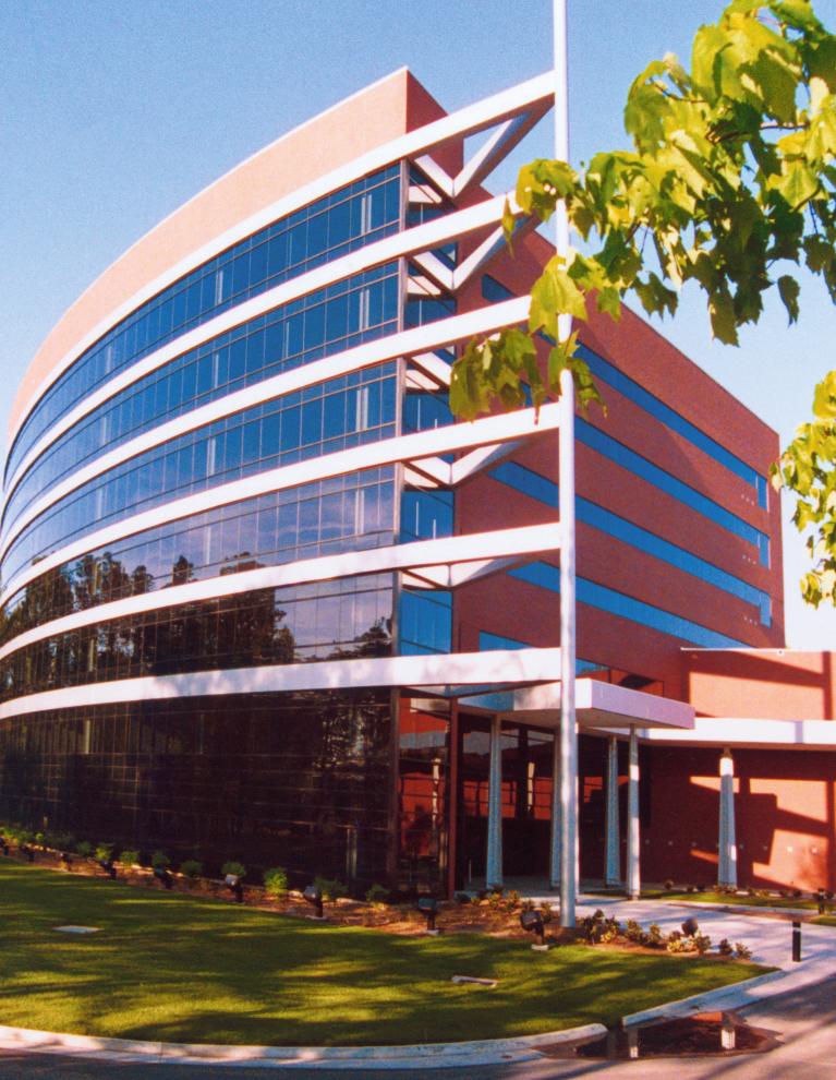
5 The Applied Research Center or ARC, is the physical location for this consortium. This flagship building, constructed by the City of Newport News Economic Development Authority, marks the start of a 200 acre research park and is a symbol of cooperation and encouragement of local and regional business development. The ARC resulted from a unique collaboration between the City of Newport News, the state, the federal government and the four consortium universities. The ARC comprises 27 state-of-the art laboratories including office space, computer facilities and a technical library, concentrating the region s multidisciplinary materials processing resources to encourage productive, stimulating interaction. Classroom courses can be taught using distance learning technologies so students and faculty can stay in the building, minimizing interruptions to their research. The ARC is also home to high-tech business start-ups, a venture capital firm, and high-tech business support services including Virginia s Center for Innovative Technology, the Hampton Roads Technology Council and the Virginia Philpott Manufacturing Extension Partnership. A RESOURCE FOR THE REGION Do you need to create an advanced material, to design a device, or to make your process better, faster, lighter, or cheaper? The Applied Research Center Consortium at the Applied Research Center (ARC) in Newport News, Virginia can help you. The Consortium was formed to facilitate advanced materials processing development and commercialization in Hampton Roads. This unique consortium of universities, including Christopher Newport University, the College of William and Mary, Norfolk State University, Old Dominion University and the Department of Energy s Thomas Jefferson National Accelerator Facility (Jefferson Lab) is available to help you with a wide range of industrial problems. Our Consortium s goals are: 1) to increase the quality of research and education, 2) to investigate complex problems identified by industry; and 3) to stimulate new economic growth and employment. Having the partners share specially designed lab and office space next to the Jefferson Lab s extensive support infrastructure facilitates collaborations for our industrial clients. The Commonwealth has recognized this excellent arrangement by awarding a $2 million, 5-year grant through Virginia s Center for Innovative Technology (CIT) to develop The Center for Plasma and Photon Processing at the ARC. ARC universities also participate in other consortia including the Virginia Microelectronics Consortium, providing rapid access statewide to other Commonwealth universities and to companies with expertise in microfabrication for electronic devices. This vast array of resources helps the consortium to collaborate with industry, to solve their problems, to create useful new materials and processes, and to educate their future employees.
6 Interested in further information about our capabilities? CONTACT THE APPLIED RESEARCH CONSORTIUM BY CALLING, ING OR FAXING Bernadette Kulas, Program Manager Center For Plasma and Photon Processing Applied Research Center Jefferson Ave, Newport News, Virginia Office: (757) Fax: (757) VISIT OUR WEBSITE AT NORTH TO RICHMOND: VIRGINIA COMMONWEALTH VIRGINIA BIOTECHNOLOGY RESEARCH CENTER THE COLLEGE OF WILLIAM & MARY VIRGINIA INSTITUTE OF MARINE SCIENCE APPLIED RESEARCH CENTER JEFFERSON LAB CHRISTOPHER NEWPORT HAMPTON ROADS TECHNOLOGY INCUBATOR NASA LARC HAMPTON JOINT TRAINING ANALYSIS SIMULATION CENTER OLD DOMINION EASTERN VIRGINIA MEDICAL SCHOOL NORFOLK STATE ACKNOWLEDGEMENTS City of Newport News Economic Development Authority Virginia s Center for Innovative Technology Commonwealth of Virginia U.S. Department of Energy PHOTO CREDITS Greg Adams, Jefferson Lab EDITORIAL AND PRODUCTION Bernadette Kulas, College of William and Mary Linda Ware, Jefferson Lab Sarah Ingels, Jefferson Lab
The Department of Advanced Materials Engineering. Materials and Processes in Polymeric Microelectronics
 The Department of Advanced Materials Engineering Materials and Processes in Polymeric Microelectronics 1 Outline Materials and Processes in Polymeric Microelectronics Polymeric Microelectronics Process
Materials and Material Innovation From FP7 to Horizon 2020
 Materials and Material From FP7 to Horizon 2020 Garmisch Partenkirchen, 10 September 2012 Martin Gieb European Commission martin.gieb@ec.europa.eu DG RTD G3-Materials Unit Europe 2020 Policy Three main
Canada s National Design Network. Community Research Innovation Opportunity
 Canada s National Design Network Community Research Innovation Opportunity Over the past five years, more than 7000 researchers in the National Design Network have benefited from industrial tools, technologies,
microelectronics services high-tech requires high-precision microelectronics services
 ELECTRICAL & ELECTRONICS microelectronics services high-tech requires high-precision microelectronics services WORLDWIDE Analysis, TESTING & CERTIFICATION LOCALLY AVAILABLE worldwide Electrical and electronic
Richard Weeks Hall of Engineering. Igniting Imagination
 Richard Weeks Hall of Engineering Igniting Imagination At Rutgers School of Engineering, students dream big, imagining a future that places them at the center of discovery and innovation able to meet the
National Centre for Flexible Electronics
 National Centre for Flexible Electronics Tripartite Partnership Government FlexE Centre - A platform for a meaningful interaction between industry and academia. An interdisciplinary team that advances
Oerlikon Eldim Empowers Your Ambition. Issue 2
 Oerlikon Eldim Empowers Your Ambition Issue 2 Successful long-term OEM relationships Empowering your ambition Forward-thinking OEMs develop strong partnerships with trusted suppliers to achieve the competitive
MISSISSIPPI POLYMER INSTITUTE: Real World Solutions to Your Technical Challenges
 MISSISSIPPI POLYMER INSTITUTE: Real World Solutions to Your Technical Challenges MPI is an ISO/IEC 17025 accredited, full-service resource for polymer and material science-related industries. Established
MEDIA RELEASE FOR IMMEDIATE RELEASE 26 JULY 2016
 MEDIA RELEASE FOR IMMEDIATE RELEASE 26 JULY 2016 A*STAR S IME KICKS OFF CONSORTIA TO DEVELOP ADVANCED PACKAGING SOLUTIONS FOR NEXT-GENERATION INTERNET OF THINGS APPLICATIONS AND HIGH-PERFORMANCE WIRELESS
Scientific Highlights 2016
 Scientific Highlights 2016 Science and Technology Sector Schools and Faculties Faculty of Science Louvain School of Engineering (EPL) Faculty of Architecture, Architectural Engineering and Urban Planning
shaping global nanofuture ULTRA-PRECISE PRINTING OF NANOMATERIALS
 shaping global nanofuture ULTRA-PRECISE PRINTING OF NANOMATERIALS WHO ARE WE? XTPL S.A. is a company operating in the nanotechnology segment. The interdisciplinary team of XTPL develops on a global scale
The Center for Emerging and Innovative Sciences University of Rochester September 5, 2013
 Manufacturing Technology Roadmaps for Photonics A Proposal to the NIST Advanced Manufacturing Consortia Program (AMTech) In Support of the National Photonics Initiative The Center for Emerging and Innovative
NASA TA-12 Roadmap Review: Manufacturing and Cross Cutting
 NASA TA-12 Roadmap Review: Manufacturing and Cross Cutting Dr. Ming C. Leu Keith and Pat Bailey Missouri Distinguished Professor Director, Center for Aerospace Manufacturing Technologies Director, Intelligent
THE BIOMEDICAL ENGINEERING TEACHING & INNOVATION CENTER. at Boston University s College of Engineering
 THE BIOMEDICAL ENGINEERING TEACHING & INNOVATION CENTER at Boston University s College of Engineering The vision At Boston University s College of Engineering, we intend to create an exciting new resource
Developing for tomorrow
 Developing for tomorrow Presenting our R&D activities worldwide Introducing technology at Bekaert Research and Development is the key driver of Bekaert s technological leadership. The role of R&D is not
NanoFabrication Kingston. Seminar and Webinar January 31, 2017 Rob Knobel Associate Professor, Dept. of Physics Queen s University
 NanoFabrication Kingston Seminar and Webinar January 31, 2017 Rob Knobel Associate Professor, Dept. of Physics Queen s University What is NFK? It s a place, an team of experts and a service. The goal of
New Horizons. A new paradigm. of collaborative research
 New Horizons A new paradigm of collaborative research One of the immediate and complex challenges facing industry, business and government in Australia today is a need to increase exports, foreign investment
Marking Cutting Welding Micro Machining Additive Manufacturing
 Marking Cutting Welding Micro Machining Additive Manufacturing Slide: 1 CM-F00003 Rev 4 G4 Pulsed Fiber Laser Slide: 2 CM-F00003 Rev 4 Versatility for Industry Automotive 2D/3D Cutting Night & Day Marking
Saxony the Organic Electronics State
 Saxony the Organic Electronics State Page 1 Agenda 1. History 2. The situation today: a major cluster in Europe 3. Saxony a dynamic place to be 4. OES at your service 5. Why to join Page 2 Downtown Dresden
ENGINEERING What can I do with this degree?
 ENGINEERING What can I do with this degree? ANY DISCIPLINE Production Sales and Marketing Management Consulting Research and Development Teaching Law AEROSPACE Propulsion Fluid Mechanics Thermodynamics
INSTITUTE FOR TELECOMMUNICATIONS RESEARCH (ITR)
") INSTITUTE FOR TELECOMMUNICATIONS RESEARCH (ITR) The ITR is one of Australia s most significant research centres in the area of wireless telecommunications. SUCCESS STORIES The GSN Project The GSN Project
INSTITUTE FOR TELECOMMUNICATIONS RESEARCH (ITR) The ITR is one of Australia s most significant research centres in the area of wireless telecommunications. SUCCESS STORIES The GSN Project The GSN Project
Swastik Technocast Limited
 An ISO-9001:2015 & ISO-14001:2015 Certified Co. PRECISION INVESTMENT & SAND CASTING UNIT About Us :- Founded in August-2007 and started production in January -2008. Swastik Technocast Limited is the premier
National Science Foundation Center for Lasers and Plasmas for Advanced Manufacturing. Mool C. Gupta Applied Research Center Old Dominion University
 National Science Foundation Center for Lasers and Plasmas for Advanced Manufacturing Mool C. Gupta Applied Research Center Old Dominion University National Science Foundation Center - Center Mission -
Creating the world technology leader in surface solutions under one roof
 Creating the world technology leader in surface solutions under one roof We are the world technology leader in the growing surface solutions market. Combining the complementary strengths of Oerlikon Balzers
FICCI Suggestions for the R & D Policy of Indian Textiles Sector
 FICCI Suggestions for the R & D Policy of Indian Textiles Sector FEDERATION OF INDIAN CHAMBERS Introduction Currently, Indian Textiles sector contributes about 14% to industrial production, 4% to the GDP,
MEDIA RELEASE FOR IMMEDIATE RELEASE. 8 November 2017
 MEDIA RELEASE FOR IMMEDIATE RELEASE 8 November 2017 A*STAR IME S NEW MULTI-CHIP FAN-OUT WAFER LEVEL PACKAGING DEVELOPMENT LINE TO DRIVE INNOVATION AND GROWTH IN SEMICONDUCTOR INDUSTRY State-of-the-art
Electronics the hidden sector. Dr Kathryn Walsh Director, Electronics-enabled Products KTN
 Electronics the hidden sector Dr Kathryn Walsh Director, Electronics-enabled Products KTN Here to celebrate! The projects The Innovative electronics Manufacturing Research Centre The Industry! Why hidden?
Coatings technology overview
 Coatings technology overview Coatings technology and the chemistry of collaboration In a competitive global coatings market, the difference between merely surviving and thriving can often lie in the efficacy
The role of university science parks in business-university research collaboration
 The role of university science parks in business-university research collaboration The Dowling Review: enhancing business-university research collaboration Dr Malcolm Parry OBE, Director and CEO The Surrey
SPECIAL MORNING SESSION
 AGENDA SPECIAL MORNING SESSION 10:00 am 10:15 am RESEARCH IMPROV: THE MISSING E Dr. Yildirim Hurmuzlu, ME Professor and Event Chair Vester Hughes Auditorium, Caruth Hall 10:15 am 10:30 am REMARKS Dr. Marc
Reducing MEMS product development and commercialization time
 Reducing MEMS product development and commercialization time Introduction Fariborz Maseeh, Andrew Swiecki, Nora Finch IntelliSense Corporation 36 Jonspin Road, Wilmington MA 01887 www.intellisense.com
Nanotechnology, the infrastructure, and IBM s research projects
 Nanotechnology, the infrastructure, and IBM s research projects Dr. Paul Seidler Coordinator Nanotechnology Center, IBM Research - Zurich Nanotechnology is the understanding and control of matter at dimensions
FRAUNHOFER INSTITUTE FOR PHOTONIC MICROSYSTEMS IPMS. Application Area. Quality of Life
 FRAUNHOFER INSTITUTE FOR PHOTONIC MICROSYSTEMS IPMS Application Area Quality of Life Overlay image of visible spectral range (VIS) and thermal infrared range (LWIR). Quality of Life With extensive experience
National Instruments Accelerating Innovation and Discovery
 National Instruments Accelerating Innovation and Discovery There s a way to do it better. Find it. Thomas Edison Engineers and scientists have the power to help meet the biggest challenges our planet faces
THE ARCOR WAY: A PASSION FOR PRECISION
 THE ARCOR WAY: A PASSION FOR PRECISION 1 THE A-TEAM Our entire team is ready to take on your toughest challenges. When you work with our A-Team leaders, you can feel confident that From engineers to project
PILOT LINE FOR LARGE-AREA PRINTING OF ELECTRONIC AND PHOTONIC DEVICES. Simon Perraud, Ph.D. Vice president for European affairs
 PILOT LINE FOR LARGE-AREA PRINTING OF ELECTRONIC AND PHOTONIC DEVICES Simon Perraud, Ph.D. Vice president for European affairs ABOUT LITEN Liten is the research institute of CEA devoted to clean energy
IHP Innovations for High Performance Microelectronics
 IHP Innovations for High Performance Microelectronics IHP - Innovations for High Performance Microelectronics in Frankfurt (Oder) is known for internationally acknowledged research at the highest level.
Micro-PackS, Technology Platform. Security Characterization Lab Opening
 September, 30 th 2008 Micro-PackS, Technology Platform Security Characterization Lab Opening Members : Micro-PackS in SCS cluster From Silicium to innovative & commucating device R&D structure, gathering
INTELLECTUAL PROPERTY FINANCIAL SUPPORT
 DARE TO INNOVATE The Centre technologique en aérospatiale (CTA) is a center of applied research that offers a range of integrated services to help clients and partners increase their knowledge, productivity
About SIMTech Pre-requisites Benefits
 About SIMTech The Singapore Institute of Manufacturing Technology (SIMTech) is a research institute of the Science and Engineering Research Council (SERC) of the Agency for Science, Technology and Research
Innovative Technology for Innovative Science Hands-on in a Nanoscience Classroom
 Innovative Technology for Innovative Science Hands-on in a Nanoscience Classroom Presented by Jennifer F. Wall, Ph.D. Imaging Possibilities Optical 2 mm Electron 500 microns Atomic Force 10 microns Scanning
Proposing a European Partnership in HORIZON EUROPE
 Proposing a European Partnership in HORIZON EUROPE Helmut Dosch Chair of LEAPS ICRI 2018-4 th International Conference on Research Infrastructures VIENNA, Austria Sep 12-14, 2018 Better Science for Europe
THIS IS INNOVATION Compound Semiconductors
 THIS IS INNOVATION Compound Semiconductors E N A B L I N G This is a quiet industrial revolution, nudging forward the capabilities of the electronics which hide inside nearly every modern day device and
The Sherwin-Williams Company
 The Sherwin-Williams Company "What is Worth Doing is Worth Doing Well." Founded in 1866 in Cleveland, Ohio #1 coatings company in the Americas #3 coatings company worldwide Over 40,000 employees worldwide
Seeing the big picture, optimising the details: Solutions in plastic for demanding applications
 Seeing the big picture, optimising the details: Solutions in plastic for demanding applications Complete solutions in plastic, from concept through to series manufacture Turning ideas into reality Short
Metal additive manufacturing for industrial applications. Global network of solutions centres. Applications expertise for a wide range of industries
 Brochure: Renishaw Solutions Centres for additive manufacturing Your partner for innovative manufacturing Metal additive manufacturing for industrial applications Global network of solutions centres Applications
Laboratory Capabilities
 THE AEROSPACE CORPORATION LABORATORIES OVERVIEW 2014 Laboratory Capabilities The Aerospace Corporation 2014 The Aerospace Corporation OTR20140702104614 Mission Ensure the effective and timely development
Cross Linking Research and Education and Entrepreneurship
 Cross Linking Research and Education and Entrepreneurship MATLAB ACADEMIC CONFERENCE 2016 Ken Dunstan Education Manager, Asia Pacific MathWorks @techcomputing 1 Innovation A pressing challenge Exceptional
Innovative antimicrobial additive for building finishing materials
 Technology Offer Innovative antimicrobial additive for building finishing materials Summary A university spin-off from Latvia has developed an innovative, environmentally friendly type of antimicrobial
CAPACITIES FOR TECHNOLOGY TRANSFER
 CAPACITIES FOR TECHNOLOGY TRANSFER The Institut de Robòtica i Informàtica Industrial (IRI) is a Joint University Research Institute of the Spanish Council for Scientific Research (CSIC) and the Technical
S-BPM ONE 2009 Constitutional convention
 S-BPM ONE 2009 Constitutional convention Karlsruhe, October 22nd 2009 Host: Prof. Dr. D. Seese, KIT, Institute AIFB INSTITUTE OF APPLIED INFORMATICS AND FORMAL DESCRIPTION METHODS (AIFB) KIT University
Georgia Electronic Commerce Association. Dr. G. Wayne Clough, President Georgia Institute of Technology April 30, 2003
 Georgia Electronic Commerce Association Dr. G. Wayne Clough, President Georgia Institute of Technology April 30, 2003 Georgia Tech: Driving high-end economic development Oak Ridge National Laboratory National
Economic Impact of the Albany Cluster. Kenneth Adams President & CEO, Commissioner Empire State Development
 Economic Impact of the Albany Cluster Kenneth Adams President & CEO, Commissioner Empire State Development Governor Andrew M. Cuomo Lt. Governor Robert J. Duffy In 2010, industry shipped over $110 billion
COMPANY PRESENTATION
 COMPANY PRESENTATION Unrivalled know-how at the service of our clients Can one be passionate about PET film? We at Coveme believe so, because this is simply what 40 years of engineering polyester has taught
Funding Opportunities in Metrology Related Research
 ASEAN-EU STI Days The Association of Southeast Asian Nations European Union Science, Technology and Innovation Days Funding Opportunities in Metrology Related Research Participation of SEA countries, and
Microwave and Microelectronics
 Microwave and Microelectronics MISSION SYSTEMS 2 BAE Systems Mission Systems Microwave and Microelectronics 3 Manufacturing Success Microwave and Microelectronics Mission Systems provides manufacturing
Addressing the Innovation Imperative
 Addressing the Innovation Imperative The Role of Public Private Partnerships Pragmatic Approaches to Technology Transfer and Commercialization Belo Horizonte, Brazil November 18, 2009 Charles W. Wessner,
Manufacturing Systems Engineering Key Expertise Theme. astutewales.com
 Manufacturing Systems Engineering Key Expertise Theme astutewales.com Exploit Resources & Connectivity in the Manufacturing Process Improve quality, productivity and sustainability. The Whole Life Cycle
Space Challenges Preparing the next generation of explorers. The Program
 Space Challenges Preparing the next generation of explorers Space Challenges is the biggest free educational program in the field of space science and high technologies in the Balkans - http://spaceedu.net
Undergraduate Research Resources and Expertise at Sheridan College
 Undergraduate Research Resources and Expertise at Sheridan College Students. Faculty. Industry. Results! How can we support you? Sheridan is a renowned leader in innovation through applied learning, creative
Industrial Innovation Information Days Brussels 3-4 October 2017
 Industrial Innovation Information Days Brussels 3-4 October 2017 NMBP Programme Parallel Sessions OPEN INNOVATION TEST BEDS Calls 2018/2019 Helene CHRAYE, HoU Unit D3 DG Research & Innovation A joint presentation
Approach for Development and Commercialization of Micro and NanoTechnologies for Aerospace Applications Dr. OUDEA Coumar EADS-ST, and Member of Board
 Approach for Development and Commercialization of Micro and NanoTechnologies for Aerospace Applications Dr. OUDEA Coumar EADS-ST, and Member of Board of Directors CANEUS Organization CANEUS CANEUS began
Overview of Auburn University
 Overview of Auburn University David M. Bevly Associate Professor Director of the GPS and Vehicle Dynamics Lab dmbevly@eng.auburn.edu (334) 844-3446 Auburn RESEARCH Peaks of Excellence Seven University
Novel laser power sensor improves process control
 Novel laser power sensor improves process control A dramatic technological advancement from Coherent has yielded a completely new type of fast response power detector. The high response speed is particularly
Embraer: Brazil s pioneering aviation giant
 14 December 2017 Embraer: Brazil s pioneering aviation giant By Catherine Jewell, Communications Division, WIPO Embraer is one of the world s leading manufacturers of commercial and executive jets, with
Metrology at NRC Canada:
 Metrology at NRC Canada: An NMI in an RTO Context Alan Steele NRC Measurement Science and Standards SIM Innovation Workshop Montevideo, Uruguay November 16, 2016 NRC: Canada s Research Technology Organization
Charles Delaunay Institute. Promoting cross-cutting synergy
 montage-pochetteicd_mise en page 1 07/07/11 10:25 Page1 Charles Delaunay Promoting cross-cutting synergy The The (CDI) brings together all of the research teams within UTT (almost 120 researchers) representing
TRIUMF ACCELERATING CANADIAN BUSINESS THROUGH SCIENCE AND INNOVATION Pre-Budget Consultation
 Canada s national laboratory for particle and nuclear physics Laboratoire national canadien pour la recherche en physique nucléaire et en physique des particules TRIUMF ACCELERATING CANADIAN BUSINESS THROUGH
BOROFLOAT. The world s first floated borosilicate glass Made in Germany with IQ
 SCHOTT Technical Glass Solutions GmbH Otto-Schott-Str. 13 07745 Jena Germany Phone: +49 (0)3641/681-4686 Fax: +49 (0)3641/2888-9241 info.borofloat@schott.com www.schott.com/borofloat The world s first
Accelerated implementation of materials and surface solutions
 Fast Track Accelerated implementation of materials and surface solutions Collaboration between industry, university and GTS-institutes Page 1 February 2016 Corporate Technology Unrestricted Siemens AG
Hellenic Technology Clusters Initiative
 Hellenic Technology Clusters Initiative Develop Regionally Compete Globally Prof. Vassilios Makios v.makios@htci.gr Dr.-Ing., MPM, Jorge-A. Sanchez-P. j.sanchez@htci.gr Dr.-Ing., MPM, Nikos Vogiatzis n.vogiatzis@htci.gr
STRATEGIC ACTIVITY PLAN
 STATE FUNDED RESEARCH INSTITUTE CENTER FOR PHYSICAL SCIENCES AND TECHNOLOGY Appropriation manager code 302496128 2017-2019 STRATEGIC ACTIVITY PLAN I. MISSION AND STRATEGIC CHANGES MISSION Implementation
IC1301 -WiPE. Wireless Power Transmission for Sustainable Electronics. SWG4.1: Space Applications. 25 March 2014
 IC1301 -WiPE Wireless Power Transmission for Sustainable Electronics SWG4.1: Space Applications 25 March 2014 Alexandru Takacs CNRS LAAS, Toulouse, France University of Toulouse III Paul Sabatier, France
The Career Center. Careers For Students Majoring In. What Can I Do With A Major In Engineering?
 Careers For Students Majoring In ENGINEERING What Can I Do With A Major In Engineering? Any Engineering Discipline Production Sales and Marketing Management Consulting Research and Development Teaching
C Sensor Systems. THz System Technology and. Prof. Dr.-Ing. Helmut F. Schlaak
 THz System Technology and C Sensor Systems Prof. Dr.-Ing. Helmut F. Schlaak Fachgebiet Mikrotechnik und Elektromechanische Systeme Fachbereich Elektrotechnik und Informationstechnik Technische Universität
Arshad Mansoor, Sr. Vice President, Research & Development INNOVATION SCOUTS: EXPANDING EPRI S TECHNOLOGY INNOVATION NETWORK
 RAC Briefing 2011-1 TO: FROM: SUBJECT: Research Advisory Committee Arshad Mansoor, Sr. Vice President, Research & Development INNOVATION SCOUTS: EXPANDING EPRI S TECHNOLOGY INNOVATION NETWORK Research
Whiting School of Engineering Interdisciplinary Centers and Institutes. Education. Research. Translation.
 Whiting School of Engineering Interdisciplinary Centers and Institutes Education. Research. Translation. T HE WHITING SCHOOL OF ENGINEERING S highly focused and interdisciplinary centers and institutes
The ELI-ALPS project ELI: Extreme Light Infrastructure ALPS: Attosecond Light Pulse Source. Zsolt Fülöp
 The ELI-ALPS project ELI: Extreme Light Infrastructure ALPS: Attosecond Light Pulse Source Zsolt Fülöp Landmark World s most advanced international laser research infrastructure Selected by ESFRI in 2006
Additive manufacturing, including the finishing of surfaces
 ADDITIVE MANUFACTURING 3D PRINTING in education, research and business Additive manufacturing, including the finishing of surfaces and the examination of components that have been created, is an interdisciplinary
Who we are. was born in 2006 as Spin-Off of Politecnico of Torino. Full time people employed 8. Laboratories and facilities 300 m 2
 Who we are was born in 2006 as Spin-Off of Politecnico of Torino Full time people employed 8 Laboratories and facilities 300 m 2 Administration and offices 250 m 2 Consolidated Turnover more then 600k
The VDL high tech ecosystem. ET industry update VDL Science & Technology, Hans Priem
 The VDL high tech ecosystem ET industry update VDL Science & Technology, Hans Priem VDL Groep Established in 19 countries > 90 operating companies > 16,000 employees, privately owned Turnover > 5 billion
Innovation for success
 Innovation for success Success in the medical sector Thin film substrates for medical implants Retinal implants for Retina Implant AG, Germany Our mission: To restore sight to blind people and thus increase
Fraunhofer Institute for High frequency physics and radar techniques FHR. Unsere Kernkompetenzen
 Fraunhofer Institute for High frequency physics and radar techniques FHR Unsere Kernkompetenzen Unsere Kernkompetenzen KEY TECHnology radar 1 2 ABOUT Fraunhofer FHR As one of the largest radar research
It s not how it s made. It s how it s made to last.
 It s not how it s made. It s how it s made to last. Fort Wayne Anodizing The most advanced fully-automated industrial hard coat anodizing line. Our commitment to a superior product that s made to last
UNIVERSITE LIBRE DE BRUXELLES
 UNIVERSITE LIBRE DE BRUXELLES HORIZON 2020 Not yet launched Information subject to change HORIZON 2020 2007-----------------------2013/2014-------------------------------------2020 Horizon 2020 : 3 pillars
An Introduction to China s Science and Technology Policy
 An Introduction to China s Science and Technology Policy SHANG Yong, Ph.D. Vice Minister Ministry of Science and Technology, China and Senior Fellow Belfer Center for Science and International Affairs
COMPTAKE COMPANY PROFILE 2017
 COMPTAKE COMPANY PROFILE 2017 HEATSINK SSD DESIGN WWW.COMPTAKE.COM WWW.COMPTAKE.COM ABOUT COMPTAKE HEADQUARTER (HQ) Established in 2004 by a group of experienced thermal experts Current capital : USD 1,000,000
SAVITRIBAI PHULE PUNE UNIVERSITY
 S- 165/2014 SAVITRIBAI PHULE PUNE UNIVERSITY EXAMINATION CIRCULAR No. 165 of 2014 Programme of the M.E. 2013 Credit Pattern (Sem. I & II ) (All Branches) Examination, Nov. - 2014. Instructions to the Candidates:
Research Categories Bioenergy Machinery Transportation. Seed Science Soil Soybeans Water
 Agricultural Sciences General Ag Sciences Agricultural Economics & Policy Agricultural education International Agriculture Ag Engineering Agronomy Animal Science Biochemicals Bioenergy Machinery Transportation
A94TT- 1 O/l. TITLE: Regional Deployment of Computer-Integrated Prototype Database
 A94TT- 1 O/l TITLE: Regional Deployment of Computer-Integrated Prototype Database CODE: A94TT-10 INVESTIGATORS: Anderson, L. J., Centrallo, C., Jenkins, A. B., Walker, B., Barry, M.E. STUDENTS: Dana Peacock,
Creation of Technical University Center of Excellence
 Available online at www.sciencedirect.com ScienceDirect Procedia - Social and Behavioral Sciences 166 ( 2015 ) 235 239 International Conference on Research Paradigms Transformation in Social Sciences 2014
Pierre Brondeau Vice President, Business Group Executive Electronic Materials Regional Director - Europe Lehman Brothers Conference Call November
 Pierre Brondeau Vice President, Business Group Executive Electronic Materials Regional Director - Europe Lehman Brothers Conference Call November 2006 Forward Looking Statement The presentation today may
ISMI Industry Productivity Driver
 SEMATECH Symposium Japan September 15, 2010 Accelerating Manufacturing Productivity ISMI Industry Productivity Driver Scott Kramer VP Manufacturing Technology SEMATECH Copyright 2010 SEMATECH, Inc. SEMATECH,
MEDIA RELEASE INSTITUTE OF MICROELECTRONICS KICKS OFF COPPER WIRE BONDING CONSORTIUM II TO TACKLE COPPER INTERCONNECTS RELIABILITY ISSUES
 MEDIA RELEASE INSTITUTE OF MICROELECTRONICS KICKS OFF COPPER WIRE BONDING CONSORTIUM II TO TACKLE COPPER INTERCONNECTS RELIABILITY ISSUES 1. Singapore, 25 March, 2013 -- The Institute of Microelectronics
sensors & systems Imagine future imaging... Leti, technology research institute Contact:
 Imaging sensors & systems Imagine future imaging... Leti, technology research institute Contact: leti.contact@cea.fr From consumer markets to high-end applications smart home IR array for human activity
The SEMATECH Model: Potential Applications to PV
 Continually cited as the model for a successful industry/government consortium Accelerating the next technology revolution The SEMATECH Model: Potential Applications to PV Dr. Michael R. Polcari President
AC : THE NATIONAL PROJECT FOR THE INNOVATIVE DEVELOPMENT OF THE HIGHER ENGINEERING EDUCATION IN RUSSIA
 AC 2007-1888: THE NATIONAL PROJECT FOR THE INNOVATIVE DEVELOPMENT OF THE HIGHER ENGINEERING EDUCATION IN RUSSIA Vasili Zhurakovskiy, Russian Association of Engineering Universities Prof., Dr. of Sc., Former
Printed Electronics. Applications
 Printed Electronics Research Through University-Industry Partnerships Outline Background on Printed Electronics (PE) Corporate Partnerships Raytheon UMass Lowell Research Institute (RURI) Printed Electronics
SCANLAB Perfect Scanning
 mirrors in motion SCANLAB Perfect Scanning Galvanometer scanners High-performance laser scan systems Objectives and focusing units Components for system integration Software Customer-specific system development
FIBER LASERS Ytterbium, Thulium and Erbium short pulse and CW lasers
 About V-Gen V-Gen develops, manufactures and markets high quality innovative laser systems for a wide range of industrial applications. The company s laser systems are the product of extensive experience