Nanoscale Systems for Opto-Electronics
|
|
|
- Eleanor Audrey Harrison
- 6 years ago
- Views:
Transcription


1 Nanoscale Systems for Opto-Electronics 675 PL intensity [arb. units] 700 Wavelength [nm] µm Energy [ev]
2 Nanoscale Systems for Opto-Electronics Lecture 5 Interaction of Light with Nanoscale Systems - general introdcution and motivation - nano-metals (Au, Ag, Cu, Al...) introduction to optical properties mie scattering mie scattering in the near-field mie scattering with nano rods resonant optical antennas - artificial quantum structures (semiconductor quantum dots,...) - quantum dot lasers Optical Interactions between Nanoscale Systems - Förster energy transfer (dipole-dipole interaction) - super-emitter concept - SERS (surface enhanced Raman spectroscopy: bio-sensors) Beating the diffraction limit with Nanoscale Systems - surface plasmon polariton (SPP) - light confinement at nanoscale - plasmonic chips - plasmonic nanolithography 2
3 Last Time: Basic Architecture of Dipole Antenna transmission line ~U feed gap antenna arms of length L perfect metal wires emitting / receiving antenna 3
4 Last Time: RLC Series Curcuit representing Dipole Antenna V0cosωt ω= 1 LC At resonance V Z= 0 j0 Z = R + ix R = Rrad + ROhm ω= 1 LC Z=R C( z) = ε 0 z L( z ) = µ0 z Xc = XL phase ϕ = 0 Q= L CR 2 4
5 Last Time: Linear Center-fed Dipole Antenna power P transmitted as e.m. wave: 1 V02 1 V02 P= Z = ( R + ix ) 2 Z2 2 Z2 R = Rrad + ROhm Summary: antenna resonance exists once the feed gap current density is high and in phase the the driving excitation field 5
 Maximum field enhancement for half-wave antenna (L ~ λ/2) 6")
6 Last Time: Antenna Feed Gap Confinement and Enhancement Half-wave antenna Full-wave antenna I(z) I(z) ρ(z) ρ(z) I(z) λ/4 λ/4 E0 L = λ/2 z λ/2 λ/2 L=λ Strength of field enhancement depends on current density j(z) Maximum field enhancement for half-wave antenna (L ~ λ/2) 6 z
")
7 Introduction: Resonant Optical Antennae antennas as receivers cover art Science 308 (2005)


8 Scaling Radio wave antenna: f ~ 1 MHz λ ~ 400 m ~ 200 m Optical antenna: f ~ 1000 THz λ ~ 400 nm Nanofabrication X 10-9 ~ 200 nm SEM image 8
9 Scaling - what is different for antennas at optical frequencies 1. Skin depth 2. Localized surface plasmons Influence on the current distribution 9
10 Skin Depth (δ) E0 E(x) Metal x 10
11 Skin Depth (δ) E0 E(x) Metal x 1 λ δ= = α 4πk absorption coefficent 11


12 Skin Depth Radio Wave Antenna E0 e. m. fields can be assumed to be restricted to the outside of an antenna Optical Antenna E0 e. m. fields are no longer restricted to the outside of an antenna 12


13 FDTD Simulation case: Al dipole antenna λex = 830 nm Finite-Difference Time-Domain Estimate effective wavelength: λ eff/2 ~ λ/2(nglass + nair) = 330 nm 13


14 Particle Plasmon Resonance Quasi-static limit: Particles smaller than the skin depth of metal E Field enhancement is determined only by the material properties, not the size of the particle - but smaller particles give more confinement Field enhancement ~ 20 on the surface (for gold) 14
15 Dielectric function of gold Re[ε ]=-2 15

16 Localized Surface Plasmons quasi-static approximation for elliptical particles: a, b, c << λ z c a b Minimize : ε1 x y εm Polarizability (a.u.) L Plasmon resonance are expected for aluminium gold rods in the NIR; α Dielectric ( L,ω ) function of gold c = b =20 nm; λ = 830 nm and aluminum gold Length L (nm) 16
17 Summarizing: Scaling Effects Large skin depth - change of boundary conditions Localized surface plasmons-resonance of the current due to a resonance in the polarizability Influence on antenna performance at optical frequencies efficiency and resonance length? 17
18 Experimental Approach Prove antenna resonance: vary only one parameter overall length L, fixed wavelength Prove field enhancement in the feed gap: use non-linear processes e.g. two photon-excited Photoluminescence M. R. Beversluis, A. Bouhelier, L. Novotny, Phys. Rev. B 68, (2003). P. J. Schuck, D. P. Fromm, A. Compare rods with antennas Sundaramurthy, G. S. Kino, W. E. Moerner, 94, (2005). no feedgap Phys. Rev. Lett. feedgap 18
19 Fabrication of Optical Antennas I. Electron beam lithography, metallization and lift off electron beam gold (40 nm) resist ITO (10nm) glass cover slip 19

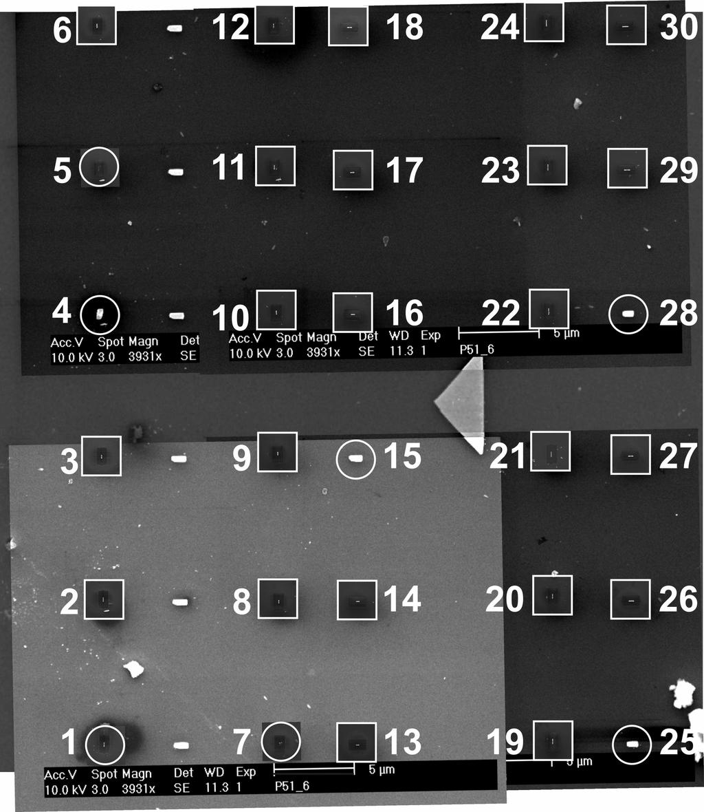
20 Fabrication of Optical Antennas Result of e-beam lithograph, metallization and lift off 50 µ m SEM Patch dimensions: 40 nm x 400 nm x 800 nm 200 nm AFM Surface roughness: ~1 nm rms 20


21 Fabrication of Optical Antennas II. Focused ion-beam milling antennas & rods Analysis by SEM and AFM 200 nm SEM AFM 21


22 Sample Antennas & rods in various length rods 19 antennas x 2.5 µ m2 22
 notch (830)")
 optical fiber & fiber")
23 Experimental Setup photodiode bandpass (600/300) notch (830) polarizer neutral density bandpass (830/10) optical fiber & fiber polarizer 23
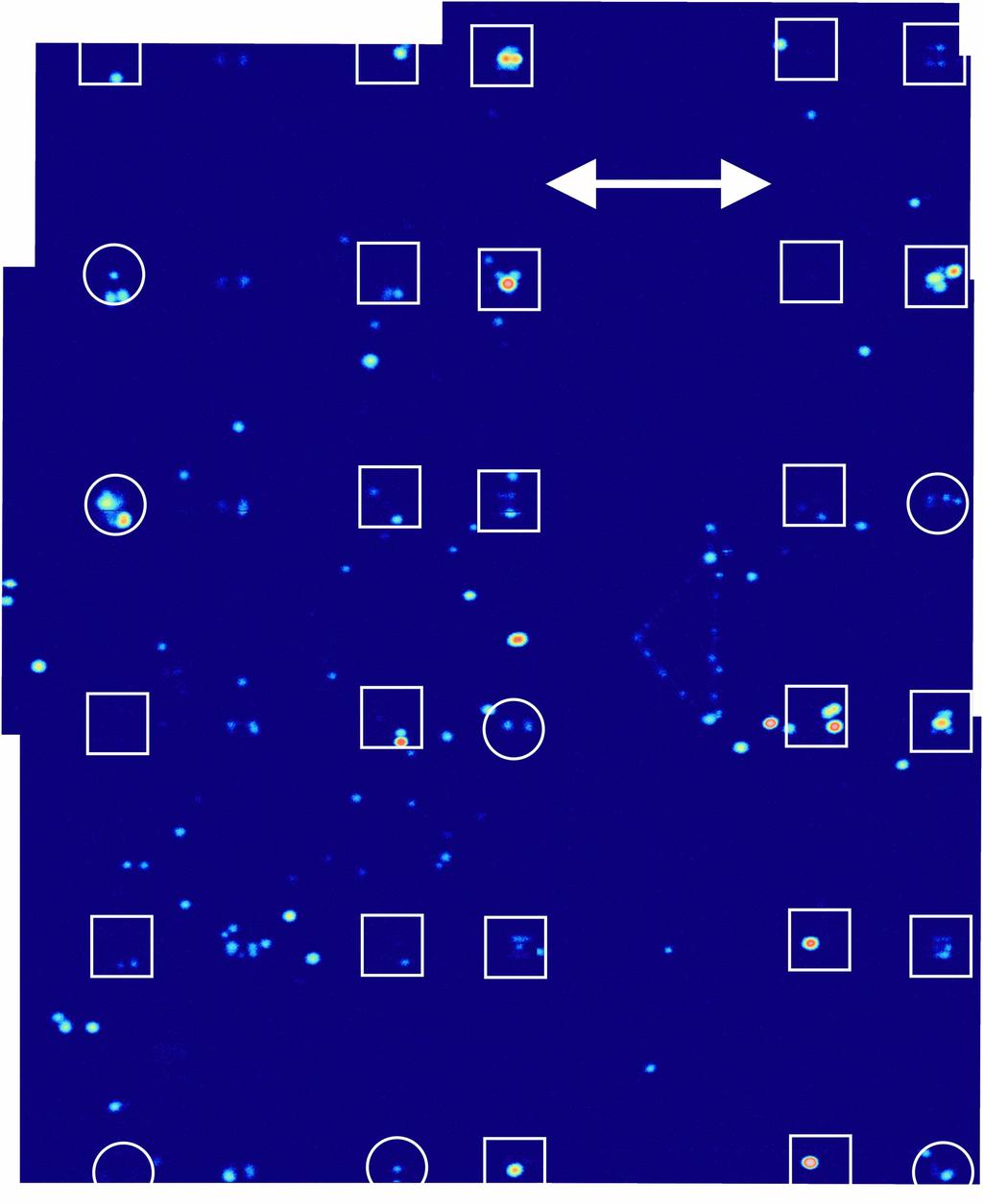
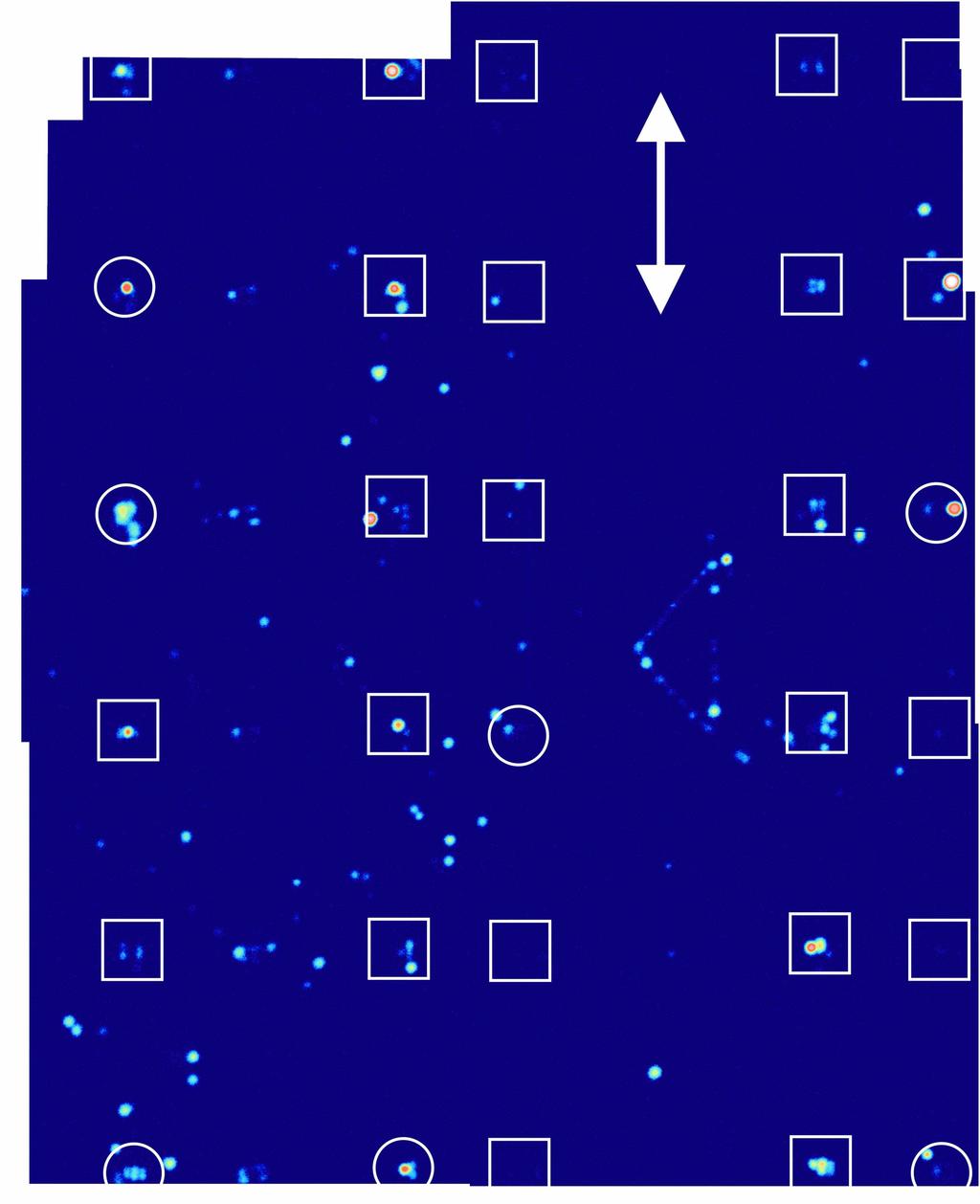
24 Measurements: Confocal experiment Log. Scale! 20 µ m 24

25 Polarization excitation polarization emission polarization (excitation under 45 ) 25
26 Results Only optical antennas in a limited length range show strong white-light continuum emission upon illumination with ps pulses White light generation only for an incident polarization along the antenna long axes 26
27 Spectrum 830 nm, FWHM 8 ps Intensity (a.u.) 2 # µw 80 µw 40 µw M. R. Beversluis, A. Bouhelier, L. Novotny, Phys. Rev. B 68, (2003). x Wavelength (nm) 27
28 Sl op e 2 Sl op e 2 Slo pe Slo pe 4 4 Power Dependence 28
29 White-Light Supercontinuum Precondition: High localization of e. m. fields in space and time strong non-linear optical interaction Characteristic: Intensity threshold ~ 1 GW/cm2 (glass, water) e.g. water ~ 10 GW/cm2 (air) Abrupt spectral broadening Kandidov et al., Appl. Phys. B 77, 149 (2003) 29
30 Slo pe Slo pe 4 4 Power Dependence 2 Estimated field enhancement factor: > 100 Sl op e Sl op e 2 Laser focus peak power at threshold: ~ 0.01 GW/cm2 30
 Simulations performed by Prof. O. J. F. Martin (EPFL) using Green s tensor technique [M. Paulus, O. J. F. Martin, J. Opt. Soc. Am. A 18, 854 (2001)].")
31 Near-field Simulations z H = 50 nm y Antenna dimensions : 40 nm x 40 nm x L x L/2 200 L/2 E0 Near-field intensity distribution X 200 nm Integration 0 R(L) Simulations performed by Prof. O. J. F. Martin (EPFL) using Green s tensor technique [M. Paulus, O. J. F. Martin, J. Opt. Soc. Am. A 18, 854 (2001)]. 31


")
32 Resonant Optical Antennas Near-field int. enhancement nm 0 4 μw μw μw R(L) 2 R(L). 32
33 Comparison: Au and Al Dipole Antenna 33
34 Results Only optical antennas in a limited length range show strong white-light continuum emission upon illumination with ps pulses White light generation only for an incident polarization along the antenna axes White-light supercontinuum generation at very low threshold intensity (~ 0.01 GW/cm2); estimated field enhancement factor > 100 Experiment and computer simulation show both similar antenna resonance length L ( ~ 250 nm) considerably shorter than λ/2 Calculated field enhancement factor in antenna feed gap >
35 Summary/Conclusion Fabrication of nanometer-scale gold dipole antennas Strong field enhancement in the antenna feed gap white-light supercontinuum generation. Resonance length of a gold antenna is considerably shorter than one-half of the wavelength of the incident light. The high field enhancement and strong resonance shift of a gold dipole antenna compared to that of aluminum antenna may be explained by surface plasmon resonance. 35
Spontaneous Hyper Emission: Title of Talk
 Spontaneous Hyper Emission: Title of Talk Enhanced Light Emission by Optical Antennas Ming C. Wu University of California, Berkeley A Science & Technology Center Where Our Paths Crossed Page Nanopatch
Contact optical nanolithography using nanoscale C-shaped apertures
 Contact optical nanolithography using nanoscale C-shaped s Liang Wang, Eric X. Jin, Sreemanth M. Uppuluri, and Xianfan Xu School of Mechanical Engineering, Purdue University, West Lafayette, Indiana 47907
Nanolithography using high transmission nanoscale ridge aperture probe
 Purdue University Purdue e-pubs Birck and NCN Publications Birck Nanotechnology Center 12-2008 Nanolithography using high transmission nanoscale ridge aperture probe Nicholas Murphy-DuBay Purdue University
SUPPLEMENTARY INFORMATION
 SUPPLEMENTARY INFORMATION DOI: 10.1038/NNANO.2015.137 Controlled steering of Cherenkov surface plasmon wakes with a one-dimensional metamaterial Patrice Genevet *, Daniel Wintz *, Antonio Ambrosio *, Alan
Nd:YSO resonator array Transmission spectrum (a. u.) Supplementary Figure 1. An array of nano-beam resonators fabricated in Nd:YSO.
 Supplementary Figure 1. An array of nano-beam resonators fabricated in Nd:YSO.") a Nd:YSO resonator array µm Transmission spectrum (a. u.) b 4 F3/2-4I9/2 25 2 5 5 875 88 λ(nm) 885 Supplementary Figure. An array of nano-beam resonators fabricated in Nd:YSO. (a) Scanning electron microscope
a Nd:YSO resonator array µm Transmission spectrum (a. u.) b 4 F3/2-4I9/2 25 2 5 5 875 88 λ(nm) 885 Supplementary Figure. An array of nano-beam resonators fabricated in Nd:YSO. (a) Scanning electron microscope
Nanopatterning using NSOM probes integrated with high transmission nanoscale bowtie aperture
 Nanopatterning using NSOM probes integrated with high transmission nanoscale bowtie aperture Nicholas Murphy-DuBay, Liang Wang, Edward C. Kinzel, Sreemanth M. V. Uppuluri, and X. Xu * School of Mechanical
COMPARATIVE ANALYSIS OF BOW-TIE AND DIPOLE NANOANTENNAS
 http:// COMPARATIVE ANALYSIS OF BOW-TIE AND DIPOLE NANOANTENNAS Manpreet Singh 1, Parminder Luthra 2 1 P.G Student, Department of Nanotechnology, BMSCE, Muktsar, Punjab, (India) 2 A.P, Department of Nanotechnology,
Instruction manual and data sheet ipca h
 1/15 instruction manual ipca-21-05-1000-800-h Instruction manual and data sheet ipca-21-05-1000-800-h Broad area interdigital photoconductive THz antenna with microlens array and hyperhemispherical silicon
Waveguiding in PMMA photonic crystals
 ROMANIAN JOURNAL OF INFORMATION SCIENCE AND TECHNOLOGY Volume 12, Number 3, 2009, 308 316 Waveguiding in PMMA photonic crystals Daniela DRAGOMAN 1, Adrian DINESCU 2, Raluca MÜLLER2, Cristian KUSKO 2, Alex.
Direct observation of beamed Raman scattering
 Supporting Information Direct observation of beamed Raman scattering Wenqi Zhu, Dongxing Wang, and Kenneth B. Crozier* School of Engineering and Applied Sciences, Harvard University, Cambridge, Massachusetts
Femtosecond laser microfabrication in. Prof. Dr. Cleber R. Mendonca
 Femtosecond laser microfabrication in polymers Prof. Dr. Cleber R. Mendonca laser microfabrication focus laser beam on material s surface laser microfabrication laser microfabrication laser microfabrication
plasmonic nanoblock pair
 Nanostructured potential of optical trapping using a plasmonic nanoblock pair Yoshito Tanaka, Shogo Kaneda and Keiji Sasaki* Research Institute for Electronic Science, Hokkaido University, Sapporo 1-2,
Enhanced transmission in near-field imaging of layered plasmonic structures
 Enhanced transmission in near-field imaging of layered plasmonic structures Reuben M. Bakker, Vladimir P. Drachev, Hsiao-Kuan Yuan and Vladimir M. Shalaev School of Electrical and Computer Engineering,
FEM simulations of nanocavities for plasmon lasers
 FEM simulations of nanocavities for plasmon lasers S.Burger, L.Zschiedrich, J.Pomplun, F.Schmidt Zuse Institute Berlin JCMwave GmbH 6th Workshop on Numerical Methods for Optical Nano Structures ETH Zürich,
Horizontal single and multiple slot waveguides: optical transmission at λ = 1550 nm
 Horizontal single and multiple slot waveguides: optical transmission at λ = 1550 nm Rong Sun 1 *, Po Dong 2 *, Ning-ning Feng 1, Ching-yin Hong 1, Jurgen Michel 1, Michal Lipson 2, Lionel Kimerling 1 1Department
Lecture 19 Optical Characterization 1
 Lecture 19 Optical Characterization 1 1/60 Announcements Homework 5/6: Is online now. Due Wednesday May 30th at 10:00am. I will return it the following Wednesday (6 th June). Homework 6/6: Will be online
High-Resolution Bubble Printing of Quantum Dots
 SUPPORTING INFORMATION High-Resolution Bubble Printing of Quantum Dots Bharath Bangalore Rajeeva 1, Linhan Lin 1, Evan P. Perillo 2, Xiaolei Peng 1, William W. Yu 3, Andrew K. Dunn 2, Yuebing Zheng 1,*
REPORT DOCUMENTATION PAGE
 REPORT DOCUMENTATION PAGE Form Approved OMB No. 0704-0188 Public reporting burden for this collection of information is estimated to average 1 hour per response, including the time for reviewing instructions,
Optimization of supercontinuum generation in photonic crystal fibers for pulse compression
 Optimization of supercontinuum generation in photonic crystal fibers for pulse compression Noah Chang Herbert Winful,Ted Norris Center for Ultrafast Optical Science University of Michigan What is Photonic
Lab4 Hanbury Brown and Twiss Setup. Photon Antibunching
 Lab4 Hanbury Brown and Twiss Setup. Photon Antibunching Shule Li Abstract Antibunching is a purely quantum effect and cannot be realized from the classical theory of light. By observing the antibunching
Cavity QED with quantum dots in semiconductor microcavities
 Cavity QED with quantum dots in semiconductor microcavities M. T. Rakher*, S. Strauf, Y. Choi, N.G. Stolz, K.J. Hennessey, H. Kim, A. Badolato, L.A. Coldren, E.L. Hu, P.M. Petroff, D. Bouwmeester University
Numerical study of optical nanolithography using nanoscale bow-tie shaped nano-apertures
 Journal of Microscopy, Vol. 229, Pt 3 2008, pp. 483 489 Received 26 September 2006; accepted 16 June 2007 Numerical study of optical nanolithography using nanoscale bow-tie shaped nano-apertures L. WANG
SUPPLEMENTARY INFORMATION Polarization response of nanowires à la carte
 * Correspondence to anna.fontcuberta-morral@epfl.ch SUPPLEMENTARY INFORMATION Polarization response of nanowires à la carte Alberto Casadei, Esther Alarcon Llado, Francesca Amaduzzi, Eleonora Russo-Averchi,
FIBER OPTICS. Prof. R.K. Shevgaonkar. Department of Electrical Engineering. Indian Institute of Technology, Bombay. Lecture: 37
 FIBER OPTICS Prof. R.K. Shevgaonkar Department of Electrical Engineering Indian Institute of Technology, Bombay Lecture: 37 Introduction to Raman Amplifiers Fiber Optics, Prof. R.K. Shevgaonkar, Dept.
Examination Optoelectronic Communication Technology. April 11, Name: Student ID number: OCT1 1: OCT 2: OCT 3: OCT 4: Total: Grade:
 Examination Optoelectronic Communication Technology April, 26 Name: Student ID number: OCT : OCT 2: OCT 3: OCT 4: Total: Grade: Declaration of Consent I hereby agree to have my exam results published on
Supporting Information
 Supporting Information Mode imaging and selection in strongly coupled nanoantennas Jer-Shing Huang 1,*, Johannes Kern 1, Peter Geisler 1, Pia Weimann 2, Martin Kamp 2, Alfred Forchel 2, Paolo Biagioni
Nano Scale Optics with Nearfield Scanning Optical Microscopy (NSOM)
") Nano Scale Optics with Nearfield Scanning Optical Microscopy (NSOM) Presentation Overview Motivation for nearfield optics Introduction to NSOM What is NSOM today? What can you do with NSOM? November 2,
Nano Scale Optics with Nearfield Scanning Optical Microscopy (NSOM) Presentation Overview Motivation for nearfield optics Introduction to NSOM What is NSOM today? What can you do with NSOM? November 2,
Administrative details:
 Administrative details: Anything from your side? www.photonics.ethz.ch 1 What are we actually doing here? Optical imaging: Focusing by a lens Angular spectrum Paraxial approximation Gaussian beams Method
Optical Fiber Technology. Photonic Network By Dr. M H Zaidi
 Optical Fiber Technology Numerical Aperture (NA) What is numerical aperture (NA)? Numerical aperture is the measure of the light gathering ability of optical fiber The higher the NA, the larger the core
Optically reconfigurable balanced dipole antenna
 Loughborough University Institutional Repository Optically reconfigurable balanced dipole antenna This item was submitted to Loughborough University's Institutional Repository by the/an author. Citation:
SUPPLEMENTARY INFORMATION
 SUPPLEMENTARY INFORMATION doi:10.1038/nature10864 1. Supplementary Methods The three QW samples on which data are reported in the Letter (15 nm) 19 and supplementary materials (18 and 22 nm) 23 were grown
SUPPLEMENTARY INFORMATION
 DOI: 1.138/NPHOTON.212.11 Supplementary information Avalanche amplification of a single exciton in a semiconductor nanowire Gabriele Bulgarini, 1, Michael E. Reimer, 1, Moïra Hocevar, 1 Erik P.A.M. Bakkers,
Numerical simulation of surface-plasmonassisted
 Numerical simulation of surface-plasmonassisted nanolithography D. B. Shao and S. C. Chen Department of Mechanical Engineering, the University of Texas at Austin, Austin, Texas 78712 scchen@mail.utexas.edu
SUPPLEMENTARY INFORMATION
 SUPPLEMENTARY INFORMATION Supplementary Information Real-space imaging of transient carrier dynamics by nanoscale pump-probe microscopy Yasuhiko Terada, Shoji Yoshida, Osamu Takeuchi, and Hidemi Shigekawa*
Supplementary Information
 Supplementary Information Atomically flat single crystalline gold nanostructures for plasmonic nanocircuitry Jer Shing Huang 1,*, Victor Callegari 2, Peter Geisler 1, Christoph Brüning 1, Johannes Kern
Continuum White Light Generation. WhiteLase: High Power Ultrabroadband
 Continuum White Light Generation WhiteLase: High Power Ultrabroadband Light Sources Technology Ultrafast Pulses + Fiber Laser + Non-linear PCF = Spectral broadening from 400nm to 2500nm Ultrafast Fiber
Supporting information: Functional plasmonic nano-circuits with low insertion and propagation losses
 Supporting information: Functional plasmonic nano-circuits with low insertion and propagation losses Arian Kriesch,,, Stanley P. Burgos, Daniel Ploss, Hannes Pfeifer, Harry A. Atwater, and Ulf Peschel
This document is downloaded from DR-NTU, Nanyang Technological University Library, Singapore.
 This document is downloaded from DR-NTU, Nanyang Technological University Library, Singapore. Title Classical imaging theory of a microlens with superresolution Author(s) Duan, Yubo; Barbastathis, George;
Influence of dielectric substrate on the responsivity of microstrip dipole-antenna-coupled infrared microbolometers
 Influence of dielectric substrate on the responsivity of microstrip dipole-antenna-coupled infrared microbolometers Iulian Codreanu and Glenn D. Boreman We report on the influence of the dielectric substrate
Investigation of the Near-field Distribution at Novel Nanometric Aperture Laser
 Investigation of the Near-field Distribution at Novel Nanometric Aperture Laser Tiejun Xu, Jia Wang, Liqun Sun, Jiying Xu, Qian Tian Presented at the th International Conference on Electronic Materials
Silicon-based photonic crystal nanocavity light emitters
 Silicon-based photonic crystal nanocavity light emitters Maria Makarova, Jelena Vuckovic, Hiroyuki Sanda, Yoshio Nishi Department of Electrical Engineering, Stanford University, Stanford, CA 94305-4088
A World of Color. Session 5 Colors of Things. OLLI at Illinois Spring D. H. Tracy
 A World of Color Session 5 Colors of Things OLLI at Illinois Spring 2018 D. H. Tracy Course Outline 1. Overview, History and Spectra 2. Nature and Sources of Light 3. Eyes and Color Vision 4. Color Spaces
Single Photon Transistor. Brad Martin PH 464
 Single Photon Transistor Brad Martin PH 464 Brad Martin Single Photon Transistor 1 Abstract The concept of an optical transistor is not a new one. The difficulty with building optical devices that use
Photomixer as a self-oscillating mixer
 Photomixer as a self-oscillating mixer Shuji Matsuura The Institute of Space and Astronautical Sciences, 3-1-1 Yoshinodai, Sagamihara, Kanagawa 9-8510, Japan. e-mail:matsuura@ir.isas.ac.jp Abstract Photomixing
Lecture 6 Fiber Optical Communication Lecture 6, Slide 1
 Lecture 6 Optical transmitters Photon processes in light matter interaction Lasers Lasing conditions The rate equations CW operation Modulation response Noise Light emitting diodes (LED) Power Modulation
Supporting Information: Plasmonic and Silicon Photonic Waveguides
 Supporting Information: Efficient Coupling between Dielectric-Loaded Plasmonic and Silicon Photonic Waveguides Ryan M. Briggs, *, Jonathan Grandidier, Stanley P. Burgos, Eyal Feigenbaum, and Harry A. Atwater,
Lecture 4 INTEGRATED PHOTONICS
 Lecture 4 INTEGRATED PHOTONICS What is photonics? Photonic applications use the photon in the same way that electronic applications use the electron. Devices that run on light have a number of advantages
Lecture 5. SPR Sensors: Principle and Instrumentation.
 Lecture 5 Optical sensors. SPR Sensors: Principle and Instrumentation. t ti Optical sensors What they can be based on: Absorption spectroscopy (UV-VIS, VIS IR) Fluorescence/phosphorescence spectroscopy
Reduction of Mutual Coupling in Closely Spaced Strip Dipole Antennas with Elliptical Metasurfaces. Hossein M. Bernety and Alexander B.
 Reduction of Mutual Coupling in Closely Spaced Strip Dipole Antennas with Elliptical Metasurfaces Hossein M. Bernety and Alexander B. Yakovlev Department of Electrical Engineering Center for Applied Electromagnetic
A NOVEL EPSILON NEAR ZERO (ENZ) TUNNELING CIRCUIT USING MICROSTRIP TECHNOLOGY FOR HIGH INTEGRABILITY APPLICATIONS
 TUNNELING CIRCUIT USING MICROSTRIP TECHNOLOGY FOR HIGH INTEGRABILITY APPLICATIONS") Progress In Electromagnetics Research C, Vol. 15, 65 74, 2010 A NOVEL EPSILON NEAR ZERO (ENZ) TUNNELING CIRCUIT USING MICROSTRIP TECHNOLOGY FOR HIGH INTEGRABILITY APPLICATIONS D. V. B. Murthy, A. Corona-Chávez
Progress In Electromagnetics Research C, Vol. 15, 65 74, 2010 A NOVEL EPSILON NEAR ZERO (ENZ) TUNNELING CIRCUIT USING MICROSTRIP TECHNOLOGY FOR HIGH INTEGRABILITY APPLICATIONS D. V. B. Murthy, A. Corona-Chávez
Antenna-like plasmon resonances of single gold nanowires in the. mid-infrared. Frank Neubrech. SERS roundtable Universität Heidelberg
 Antenna-like plasmon resonances of single gold nanowires in the mid-infrared SERS roundtable 2006 Frank Neubrech Kirchhoff-Institut für Physik Universität Heidelberg Outline Introduction Experimental setup
Supplementary Figure 1. Effect of the spacer thickness on the resonance properties of the gold and silver metasurface layers.
 Supplementary Figure 1. Effect of the spacer thickness on the resonance properties of the gold and silver metasurface layers. Finite-difference time-domain calculations of the optical transmittance through
Research of photolithography technology based on surface plasmon
 Research of photolithography technology based on surface plasmon Li Hai-Hua( ), Chen Jian( ), and Wang Qing-Kang( ) National Key Laboratory of Micro/Nano Fabrication Technology, Key Laboratory for Thin
Self-phase-modulation induced spectral broadening in silicon waveguides
 Self-phase-modulation induced spectral broadening in silicon waveguides Ozdal Boyraz, Tejaswi Indukuri, and Bahram Jalali University of California, Los Angeles Department of Electrical Engineering, Los
Comparative Study of Radiation Pattern of Some Different Type Antennas
 International Journal of Physics and Applications. ISSN 974-313 Volume 6, Number 2 (214), pp. 19-114 International Research Publication House http://www.irphouse.com Comparative Study of Radiation Pattern
High-Q surface plasmon-polariton microcavity
 Chapter 5 High-Q surface plasmon-polariton microcavity 5.1 Introduction As the research presented in this thesis has shown, microcavities are ideal vehicles for studying light and matter interaction due
Guided Propagation Along the Optical Fiber. Xavier Fernando Ryerson University
 Guided Propagation Along the Optical Fiber Xavier Fernando Ryerson University The Nature of Light Quantum Theory Light consists of small particles (photons) Wave Theory Light travels as a transverse electromagnetic
Introduction to Optoelectronic Devices
 Introduction to Optoelectronic Devices Dr. Jing Bai Assistant Professor Department of Electrical and Computer Engineering University of Minnesota Duluth October 30th, 2012 1 Outline What is the optoelectronics?
Waveguide Bragg Gratings and Resonators LUMERICAL SOLUTIONS INC
 Waveguide Bragg Gratings and Resonators JUNE 2016 1 Outline Introduction Waveguide Bragg gratings Background Simulation challenges and solutions Photolithography simulation Initial design with FDTD Band
photolithographic techniques (1). Molybdenum electrodes (50 nm thick) are deposited by
. Molybdenum electrodes (50 nm thick) are deposited by") Supporting online material Materials and Methods Single-walled carbon nanotube (SWNT) devices are fabricated using standard photolithographic techniques (1). Molybdenum electrodes (50 nm thick) are deposited
Supporting online material Materials and Methods Single-walled carbon nanotube (SWNT) devices are fabricated using standard photolithographic techniques (1). Molybdenum electrodes (50 nm thick) are deposited
Chiral Surface Plasmon Polaritons on Metallic Nanowires
 Chiral Surface Plasmon Polaritons on Metallic Nanowires Shunping Zhang, 1 Hong Wei, 1 Kui Bao, 2 Ulf Håkanson, 1,4 Naomi J. Halas, 1,2,3 Peter Nordlander, 1,2 and Hongxing Xu 1,4,* 1 Beijing National Laboratory
Supporting Information
 Electronic Supplementary Material (ESI) for Materials Horizons. This journal is The Royal Society of Chemistry 2017 Supporting Information Nanofocusing of circularly polarized Bessel-type plasmon polaritons
Design, Fabrication and Characterization of Very Small Aperture Lasers
 372 Progress In Electromagnetics Research Symposium 2005, Hangzhou, China, August 22-26 Design, Fabrication and Characterization of Very Small Aperture Lasers Jiying Xu, Jia Wang, and Qian Tian Tsinghua
Optoelectronics ELEC-E3210
 Optoelectronics ELEC-E3210 Lecture 4 Spring 2016 Outline 1 Lateral confinement: index and gain guiding 2 Surface emitting lasers 3 DFB, DBR, and C3 lasers 4 Quantum well lasers 5 Mode locking P. Bhattacharya:
Photonic Crystals for Confining, Guiding, and Emitting Light
 4 IEEE TRANSACTIONS ON NANOTECHNOLOGY, VOL. 1, NO. 1, MARCH 2002 Photonic Crystals for Confining, Guiding, and Emitting Light Axel Scherer, Oskar Painter, Jelena Vuckovic, Marko Loncar, and Tomoyuki Yoshie
Attosecond technology - quantum control of high harmonic generation for phase matching
 Attosecond technology - quantum control of high harmonic generation for phase matching Xiaoshi Zhang, Amy Lytle, Oren Cohen, Ivan P. Christov, Margaret M. Murnane, Henry C. Kapteyn JILA, University of
DIELECTRIC WAVEGUIDES and OPTICAL FIBERS
 DIELECTRIC WAVEGUIDES and OPTICAL FIBERS Light Light Light n 2 n 2 Light n 1 > n 2 A planar dielectric waveguide has a central rectangular region of higher refractive index n 1 than the surrounding region
MULTI-STAGE YTTERBIUM FIBER-AMPLIFIER SEEDED BY A GAIN-SWITCHED LASER DIODE
 MULTI-STAGE YTTERBIUM FIBER-AMPLIFIER SEEDED BY A GAIN-SWITCHED LASER DIODE Authors: M. Ryser, S. Pilz, A. Burn, V. Romano DOI: 10.12684/alt.1.101 Corresponding author: e-mail: M. Ryser manuel.ryser@iap.unibe.ch
Supplementary Information:
 Supplementary Information: This document contains supplementary text discussing the methods used, figures providing information on the QD sample and level structure (Fig. S), key components of the experimental
AIR-COUPLED PHOTOCONDUCTIVE ANTENNAS
 AIR-COUPLED PHOTOCONDUCTIVE ANTENNAS Report: Air-Coupled Photoconductive Antennas In this paper, we present air-coupled terahertz photoconductive antenna (THz-PCAs) transmitters and receivers made on high-resistive
A continuous-wave Raman silicon laser
 A continuous-wave Raman silicon laser Haisheng Rong, Richard Jones,.. - Intel Corporation Ultrafast Terahertz nanoelectronics Lab Jae-seok Kim 1 Contents 1. Abstract 2. Background I. Raman scattering II.
2. Pulsed Acoustic Microscopy and Picosecond Ultrasonics
 1st International Symposium on Laser Ultrasonics: Science, Technology and Applications July 16-18 2008, Montreal, Canada Picosecond Ultrasonic Microscopy of Semiconductor Nanostructures Thomas J GRIMSLEY
Enhanced directional excitation and emission of single emitters by a nano-optical Yagi-Uda antenna.
 Enhanced directional excitation and emission of single emitters by a nano-optical Yagi-Uda antenna. Tim H. Taminiau*, Fernando D. Stefani, and Niek F. van Hulst # ICFO Institut de Ciences Fotoniques, Mediterranean
Supplementary Figure 1 Reflective and refractive behaviors of light with normal
 Supplementary Figures Supplementary Figure 1 Reflective and refractive behaviors of light with normal incidence in a three layer system. E 1 and E r are the complex amplitudes of the incident wave and
SPP waveguide sensors
 SPP waveguide sensors 1. Optical sensor - Properties - Surface plasmon resonance sensor - Long-range surface plasmon-polariton sensor 2. LR-SPP waveguide - SPP properties in a waveguide - Asymmetric double-electrode
Metal-semiconductor-metal photodetector with enhanced TE-polarization transmission
 Edith Cowan University Research Online ECU Publications 2012 2012 Metal-semiconductor-metal photodetector with enhanced TE-polarization transmission Ayman Karar Edith Cowan University, ayman_karar@hotmail.com
Supplementary Materials for
 advances.sciencemag.org/cgi/content/full/3/4/e1602570/dc1 Supplementary Materials for Toward continuous-wave operation of organic semiconductor lasers Atula S. D. Sandanayaka, Toshinori Matsushima, Fatima
Within the burgeoning field of nanotechnology, one of the
 pubs.acs.org/nanolett Direct Observation of Beamed Raman Scattering Wenqi Zhu, Dongxing Wang, and Kenneth B. Crozier* School of Engineering and Applied Sciences, Harvard University, Cambridge, Massachusetts
GaAs polytype quantum dots
 GaAs polytype quantum dots Vilgailė Dagytė, Andreas Jönsson and Andrea Troian December 17, 2014 1 Introduction An issue that has haunted nanowire growth since it s infancy is the difficulty of growing
Light management in photovoltaics using nanotechnology
 Light management in photovoltaics using nanotechnology Albert Polman Center for Nanophotonics FOM-Institute AMOLF Amsterdam, The Netherlands Solar irradiance on earth assuming 30% PV, 175 W/m 2 Solar
By emitter degradation analysis of high power diode laser bars. Outline Part I
 By emitter degradation analysis of high power diode laser bars Eric Larkins and Jens W. Tomm Outline Part I I. 1. Introduction I. 2. Experimental Techniques I. 3. Case Study 1: Strain Threshold for Increased
Dual-frequency Characterization of Bending Loss in Hollow Flexible Terahertz Waveguides
 Dual-frequency Characterization of Bending Loss in Hollow Flexible Terahertz Waveguides Pallavi Doradla a,b, and Robert H. Giles a,b a Submillimeter Wave Technology Laboratory, University of Massachusetts
Wavelength-independent coupler from fiber to an on-chip cavity, demonstrated over an 850nm span. Steven Wang, Tal Carmon, Eric Ostby and Kerry Vahala
 Wavelength-independent coupler from fiber to an on-chip, demonstrated over an 85nm span Steven Wang, Tal Carmon, Eric Ostby and Kerry Vahala Basics of coupling Importance of phase match ( λ ) 1 ( λ ) 2
Fiber Lasers for EUV Lithography
 Fiber Lasers for EUV Lithography A. Galvanauskas, Kai Chung Hou*, Cheng Zhu CUOS, EECS Department, University of Michigan P. Amaya Arbor Photonics, Inc. * Currently with Cymer, Inc 2009 International Workshop
Narrowing spectral width of green LED by GMR structure to expand color mixing field
 Narrowing spectral width of green LED by GMR structure to expand color mixing field S. H. Tu 1, Y. C. Lee 2, C. L. Hsu 1, W. P. Lin 1, M. L. Wu 1, T. S. Yang 1, J. Y. Chang 1 1. Department of Optical and
A Hertzian Plasmonic Nanodimer as an Efficient Optical. Nanoantenna
 A Hertzian Plasmonic Nanodimer as an Efficient Optical Nanoantenna Andrea Alù, and Nader Engheta * Department of Electrical and Systems Engineering, University of Pennsylvania Philadelphia, PA 19104, U.S.A.
Lecture 18: Photodetectors
 Lecture 18: Photodetectors Contents 1 Introduction 1 2 Photodetector principle 2 3 Photoconductor 4 4 Photodiodes 6 4.1 Heterojunction photodiode.................... 8 4.2 Metal-semiconductor photodiode................
NGS-13, Guildford UK, July 2007
 NGS-1, Guildford UK, July 7 Semiconductor light emitters for mid-ir spectral region -based Quantum Cascade Room temperature operated type-i QW -based light emitters with wavelength up to.4um L. Shterengas,
Lecture Notes 10 Image Sensor Optics. Imaging optics. Pixel optics. Microlens
 Lecture Notes 10 Image Sensor Optics Imaging optics Space-invariant model Space-varying model Pixel optics Transmission Vignetting Microlens EE 392B: Image Sensor Optics 10-1 Image Sensor Optics Microlens
Slot waveguide-based splitters for broadband terahertz radiation
 Slot waveguide-based splitters for broadband terahertz radiation Shashank Pandey, Gagan Kumar, and Ajay Nahata* Department of Electrical and Computer Engineering, University of Utah, Salt Lake City, Utah
Mode analysis of Oxide-Confined VCSELs using near-far field approaches
 Annual report 998, Dept. of Optoelectronics, University of Ulm Mode analysis of Oxide-Confined VCSELs using near-far field approaches Safwat William Zaki Mahmoud We analyze the transverse mode structure
Nano-structured superconducting single-photon detector
 Nano-structured superconducting single-photon detector G. Gol'tsman *a, A. Korneev a,v. Izbenko a, K. Smirnov a, P. Kouminov a, B. Voronov a, A. Verevkin b, J. Zhang b, A. Pearlman b, W. Slysz b, and R.
Opto-VLSI-based reconfigurable photonic RF filter
 Research Online ECU Publications 29 Opto-VLSI-based reconfigurable photonic RF filter Feng Xiao Mingya Shen Budi Juswardy Kamal Alameh This article was originally published as: Xiao, F., Shen, M., Juswardy,
THE PAST rapid emergence of optical microcavity devices,
 IEEE TRANSACTIONS ON NANOTECHNOLOGY, VOL. 1, NO. 1, MARCH 2002 1 Photonic Crystals for Confining, Guiding, and Emitting Light Axel Scherer, Oskar Painter, Jelena Vuckovic, Marko Loncar, and Tomoyuki Yoshie
Guided Propagation Along the Optical Fiber. Xavier Fernando Ryerson Comm. Lab
 Guided Propagation Along the Optical Fiber Xavier Fernando Ryerson Comm. Lab The Nature of Light Quantum Theory Light consists of small particles (photons) Wave Theory Light travels as a transverse electromagnetic
Microprobe-enabled Terahertz sensing applications
 Microprobe-enabled Terahertz sensing applications World of Photonics, Laser 2015, Munich Protemics GmbH Aachen, Germany Terahertz microprobing technology: Taking advantage of Terahertz range benefits without
Dielectric-lined cylindrical metallic THz waveguides: mode structure and dispersion
 Dielectric-lined cylindrical metallic THz waveguides: mode structure and dispersion Oleg Mitrofanov 1 * and James A. Harrington 2 1 Department of Electronic and Electrical Engineering, University College
Bandpass Edge Dichroic Notch & More
 Edmund Optics BROCHURE Filters COPYRIGHT 217 EDMUND OPTICS, INC. ALL RIGHTS RESERVED 1/17 Bandpass Edge Dichroic Notch & More Contact us for a Stock or Custom Quote Today! USA: +1-856-547-3488 EUROPE:
Measuring chromatic aberrations in imaging systems using plasmonic nano particles
 Measuring chromatic aberrations in imaging systems using plasmonic nano particles Sylvain D. Gennaro, Tyler R. Roschuk, Stefan A. Maier, and Rupert F. Oulton* Department of Physics, The Blackett Laboratory,
ENHANCEMENT OF PRINTED DIPOLE ANTENNAS CHARACTERISTICS USING SEMI-EBG GROUND PLANE
 J. of Electromagn. Waves and Appl., Vol. 2, No. 8, 993 16, 26 ENHANCEMENT OF PRINTED DIPOLE ANTENNAS CHARACTERISTICS USING SEMI-EBG GROUND PLANE F. Yang, V. Demir, D. A. Elsherbeni, and A. Z. Elsherbeni