SUPPLEMENTARY INFORMATION
|
|
|
- Arnold Morton
- 5 years ago
- Views:
Transcription
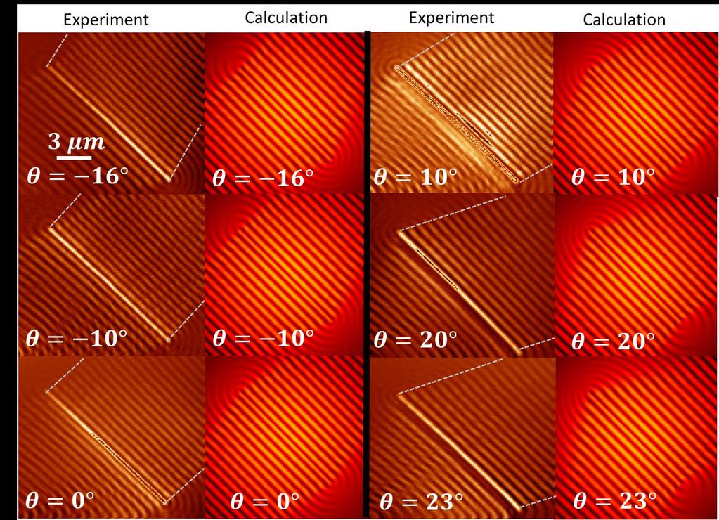
1 SUPPLEMENTARY INFORMATION DOI: /NNANO Controlled steering of Cherenkov surface plasmon wakes with a one-dimensional metamaterial Patrice Genevet *, Daniel Wintz *, Antonio Ambrosio *, Alan She, Romain Blanchard, and * These authors contributed equally. Federico Capasso 1-FULL DESCRIPTION OF THE NSOM INTERFEROGRAM OF THE SLIT CASE In our experiments, to observe SPP wavefronts (without having to set up a phase-sensitive NSOM experiment, which is a cumbersome and difficult task in the visible), we used the fact that some fraction of the incident wavefront is transmitted through the thin metallic film and interferes with the plasmons propagating on the other side of the film, as in Ref. [S4]. NSOM images obtained in our experiments show the near-field intensity of the interference pattern between surface plasmons propagating on the metal film and the transmitted light. This interference gives information on the phase distribution of the propagating SPPs. The interfringe distance is given by (Fig. S1b). By measuring, this expression is used to calculate the angle of the wakes and these are compared to the experimental values. 2- DIPOLE-LIKE DESCRIPTION OF SURFACE PLASMON POLARITON MODES IN LINEAR ROTATING APERTURE ANTENNAS 2.1 Surface plasmon polaritons from a straight aperture antenna When a surface plasmon is generated at a metal-dielectric interface by illuminating a subwavelength slit on the metallic film (straight apertured antenna), the two-dimensional evolution of the electric field (complex amplitude) in the plane can be approximated by the equation: Eq. (S1) NATURE NANOTECHNOLOGY Macmillan Publishers Limited. All rights reserved
2 where is the SPP wavenumber (neglecting any attenuation of the SPP), is the position of the aperture, is the angular orientation, and. This equation is obtained by transforming equation (2) of Ref. [S1] to follow the notation and orientation of axes introduced in Fig. S2. Fig. S2 also shows the dipole-like intensity and phase distributions of the SPPs from a straight aperture antenna oriented along the -axis computed using Eq. S1 and excited by an S- polarized source impinging at normal incidence. If more apertures are milled into the metallic surface, it is possible (neglecting near-field interactions between apertures), to consider SPPs from each antenna, as described by Eq. S1. Then the contributions from each dipole are summed up (each with phase and amplitude) to obtain the total field distribution of the surface wave. It is worth noting that, although simplistic, this approximation can still be applied to cases of practical interest 1,2. Fig. S4 shows two cases of straight aperture antennas close together, rotated by and excited by a linearly polarized beam incident at. In this case, there is no further phase delay between the antennas and the final picture is only due to the relative orientations of the apertures. In the special case of a rotationally symmetric aperture (symmetric cross or circle), illumination with circularly polarized light ( and have equal magnitudes and are phase delayed by ) results in a phase delay between the SPPs launched along the two directions (for the behavior of elliptically polarized dipoles, for example, see Ref [S3]). For this scenario, the intensity and phase distributions are reported in Fig. S5. The phase of the emitted surface plasmons covers radians around the structure. This results from the transfer of spin angular momentum of light, allowing generation of SPPs with phase coverage along the azimuthal coordinate. It is important to stress that even if the phase coverage around the symmetric aperture range between 0 to, the rotation of a symmetric element cannot be used to address a Pancharatnam-Berry phase retardation. 2.2 Surface Plasmon Polariton from a linear array of straight rotated aperture antennas In order to correctly describe the total in-plane SPP field distribution created by a linear array of straight rotated antennas arranged along an axis (Fig. S6), we need to consider a generalized version of Eq. S Macmillan Publishers Limited. All rights reserved
3 With reference to the axes represented in Fig. S6b, the electric field of the illuminating plane wave has components along the direction normal to the antenna axis: (Eq. S2) where and are the complex field amplitudes. In the experiment, the linear polarization of the illuminating beam is changed by means of a quarter waveplate. Accounting for the projection of the incident field onto the and axes, the total field in the plane due to every antenna excited by an elliptically polarized beam can be summed up as: Where: ; (Eq. S3) Eq. S3 correctly describes the field produced by a single straight aperture antenna. Note that the schematic in Fig. S6 (b) describes the case. The field emitted by an array, as presented in Fig. S6 (a), is obtained by considering a linear superposition of the field created by each individual antenna oriented as in Fig. S6. Eq. S3 correctly describes the field produced by a single straight aperture antenna. Note that the schematic in Fig. S6 (b) describes the case. The field emitted by an array, as presented in Fig. S6 (a), is obtained by considering a linear superposition of the field created by each individual antenna oriented as in Fig. S6.For the purpose of explaining the linear phase relationship between the rotation angle of the antenna and the phase delay of the radiated surface plasmons, one can simplify Eq. S3 to the case of a single antenna placed in. In this conditions the field at a generic point on the -axis ( ) is proportional to. This case is presented in Figure S7 and S8, confirming that for circularly polarized light, the phase retardation is directly given by the rotation angle of the antenna and is modulo. We confirmed the predictions of the analytical model (intensity and phase distribution) by performing full electromagnetic wave FDTD simulations. An example of the obtained simulations is presented in Fig. S8 and is in excellent agreement with the analytical model described above Macmillan Publishers Limited. All rights reserved
4 3- NSOM Imaging of the Surface Plasmon Polariton Wakes When the metallic film is thin enough, the incident beam transmits through the film and can interfere with the in-plane components of the SPP. This results in the fringe pattern that we observed in our experiment the interferogram. In fact, even though the inplane components of the SPPs are weaker than the out-of-plane one, when the NSOM is operated in collection mode with a coated tapered fiber, the NSOM preferentially detects the in-plane components of the surface waves as reported and discussed elsewhere, 4,5 and proved by the excellent agreement between our experimental data and simulations reported in the main text. Our NSOM microscope is the Multiview 4000 from Nanonics Ltd. The probe is an Au-coated bent tapered optical fiber mounted on a tuning fork. The tip-to-sample stabilization is provided by normal-force monitoring. Photons coupled into the fiber from the near-field region are detected by means of a Single Photon Avalanche Diode (SPAD) by MPD S.r.l. References and notes 1. Tanemura, T., et al. Multiple-wavelength focusing of surface plasmons with a nonperiodic nanoslit coupler. Nano Lett. 11 (2011): Tetienne, J.P., et al. Dipolar modeling and experimental demonstration of multi-beam plasmonic collimators. New J. Phys. 13 (2011): Mueller, J.P.B., & Capasso, F. Asymmetric surface plasmon polariton emission by a dipole emitter near a metal surface. Phys. Rev. B 88 (2013): Yin, L., et al. Surface plasmons at single nanoholes in Au films. Appl. Phys. Lett. 85 (2004): Bouhelier, A., et al. Surface plasmon interference excited by tightly focused laser beams. Opt. Lett. 32 (2007): Figure Captions 2015 Macmillan Publishers Limited. All rights reserved
5 Figure S1: (a) x-z schematic of the experiment and resultant electric fields on the control sample (slit). Obliquely incident free space light (wavefronts shown as thin orange lines) generates SPPs, which propagate away from the slit with wavefronts tilted at an angle. The SPP wavefronts are shown in (b) as gray lines. A purely visual representation of their interference with the incident oblique wavefront (vertical lines) is shown. This constructive interference produces an intensity pattern with iso-intensity lines parallel to the slit axis (thick grey lines). The distance between the interference fringes, denoted by, is experimentally measured and used to calculate the SPP emission angle. Figure S2. (a) Notations for the axes and antenna rotation angle ( ). (b) Calculated intensity at the metal film and (c) phase distribution of the SPPs launched by a straight aperture antenna oriented along the -axis. The scale bar length in the pictures is. Figure S3: Left: experimental NSOM data for slits with different incident angles. Right: calculated electric field distribution of the interference pattern of surface plasmon wakes excited by S-polarized light at different incident angles. The results are summarized in Fig. 2c in the main text. Figure S4: (a,d) Schematic of two (three) nano-apertures successively oriented at a angle. (b,e) Intensity and (c,f) phase distributions of the total SPP field of two (a,b,c) and three (d,e,f) straight aperture antennas illuminated by linearly polarized light and rotated with respect to each other. The scale bar length in the pictures is. Figure S5: (a) Schematic of the metallic nanohole (circular aperture). (b) Calculated intensity at the surface of the metal and (c) phase distributions of the total SPP field of a nanohole illuminated by circularly polarized light. The scale bar length in the pictures is. (d) Phase of the emitted plasmons along the red circle in (a) as a function of the angle. Figure S6: (a) Straight aperture antennas rotated by with respect to each other, whose centers are aligned along the -axis. (b) Sketch of the orientation of the illuminating electric field components with respect to a generic aperture antenna. Figure S7. (a) FDTD simulation of the intensity distribution of the SPP excited by a period array of 8 rotated antennas. (b) Real part of the out of plane field distribution. (c) Zoomed in picture of the real part of, showing that the phase at the antenna axis rotates from to in a period. All values are taken at above the gold film. (d) Analog of (b) but from the analytical model described by Eq. S3. Figure S8. a) Schematic of the antenna modeled using FDTD, with the amplitude and phase monitored at point D. b) SPP phase delay relative to the circularly polarized reference beam at point D as a function of rotation angle of the antenna. The phase delay results are modulo Macmillan Publishers Limited. All rights reserved
6 c) Real part of the out-of-plane electric field for an array of linear aperture antennas. This is useful to visualize the dipole-like emission of the SPP from each antenna and the relative phase accumulated along the line of antennas. d) SPP intensity monitored at point D as a function of rotation angle. The normalized intensity varies from 0 to 1 as the projection of the incident electric field changes from parallel to the slit axis to perpendicular to the slit axis. Figure S9. Coupling efficiency calculated numerically as a function of beam waist. Four periods of antennas with is excited by a Gaussian beam. Efficiency is calculated by monitoring the reflection and transmission and calculating. Changing the beam waist shows that the efficiency of the device can potentially be doubled. Figure S10. In-plane electric field perpendicular to a nanoslit of various lengths as a function of wavelength. This highlights a potential method to increase the device efficiency by utilizing a plasmonic resonance Macmillan Publishers Limited. All rights reserved

7

8
9

10

11

12

13

14
15
16
Supplementary Figure 1: Optical Properties of V-shaped Gold Nanoantennas a) Illustration of the possible plasmonic modes.
 Illustration of the possible plasmonic modes.") Supplementary Figure 1: Optical Properties of V-shaped Gold Nanoantennas a) Illustration of the possible plasmonic modes. S- symmetric, AS antisymmetric. b) Calculated linear scattering spectra of individual
Supplementary Figure 1: Optical Properties of V-shaped Gold Nanoantennas a) Illustration of the possible plasmonic modes. S- symmetric, AS antisymmetric. b) Calculated linear scattering spectra of individual
Will contain image distance after raytrace Will contain image height after raytrace
 Name: LASR 51 Final Exam May 29, 2002 Answer all questions. Module numbers are for guidance, some material is from class handouts. Exam ends at 8:20 pm. Ynu Raytracing The first questions refer to the
9. Microwaves. 9.1 Introduction. Safety consideration
 MW 9. Microwaves 9.1 Introduction Electromagnetic waves with wavelengths of the order of 1 mm to 1 m, or equivalently, with frequencies from 0.3 GHz to 0.3 THz, are commonly known as microwaves, sometimes
Investigation of the Near-field Distribution at Novel Nanometric Aperture Laser
 Investigation of the Near-field Distribution at Novel Nanometric Aperture Laser Tiejun Xu, Jia Wang, Liqun Sun, Jiying Xu, Qian Tian Presented at the th International Conference on Electronic Materials
Supplementary Information for. Surface Waves. Angelo Angelini, Elsie Barakat, Peter Munzert, Luca Boarino, Natascia De Leo,
 Supplementary Information for Focusing and Extraction of Light mediated by Bloch Surface Waves Angelo Angelini, Elsie Barakat, Peter Munzert, Luca Boarino, Natascia De Leo, Emanuele Enrico, Fabrizio Giorgis,
Polarization Experiments Using Jones Calculus
 Polarization Experiments Using Jones Calculus Reference http://chaos.swarthmore.edu/courses/physics50_2008/p50_optics/04_polariz_matrices.pdf Theory In Jones calculus, the polarization state of light is
A novel tunable diode laser using volume holographic gratings
 A novel tunable diode laser using volume holographic gratings Christophe Moser *, Lawrence Ho and Frank Havermeyer Ondax, Inc. 85 E. Duarte Road, Monrovia, CA 9116, USA ABSTRACT We have developed a self-aligned
Nanoscale Systems for Opto-Electronics
 Nanoscale Systems for Opto-Electronics 675 PL intensity [arb. units] 700 Wavelength [nm] 650 625 600 5µm 1.80 1.85 1.90 1.95 Energy [ev] 2.00 2.05 1 Nanoscale Systems for Opto-Electronics Lecture 5 Interaction
Dielectric Metasurface for Generating Broadband Millimeter Wave Orbital. Angular Momentum Beams
 Dielectric Metasurface for Generating Broadband Millimeter Wave Orbital Angular Momentum Beams Fan Bi 1,2, Zhongling Ba 2, Yunting Li 2, and Xiong Wang 2, 1 Shanghai Institute of Microsystem and Information
Symmetrically coated pellicle beam splitters for dual quarter-wave retardation in reflection and transmission
 University of New Orleans ScholarWorks@UNO Electrical Engineering Faculty Publications Department of Electrical Engineering 1-1-2002 Symmetrically coated pellicle beam splitters for dual quarter-wave retardation
A broadband achromatic metalens for focusing and imaging in the visible
 SUPPLEMENTARY INFORMATION Articles https://doi.org/10.1038/s41565-017-0034-6 In the format provided by the authors and unedited. A broadband achromatic metalens for focusing and imaging in the visible
Supporting Information: Plasmonic and Silicon Photonic Waveguides
 Supporting Information: Efficient Coupling between Dielectric-Loaded Plasmonic and Silicon Photonic Waveguides Ryan M. Briggs, *, Jonathan Grandidier, Stanley P. Burgos, Eyal Feigenbaum, and Harry A. Atwater,
Laser Beam Analysis Using Image Processing
 Journal of Computer Science 2 (): 09-3, 2006 ISSN 549-3636 Science Publications, 2006 Laser Beam Analysis Using Image Processing Yas A. Alsultanny Computer Science Department, Amman Arab University for
Deliverable Report. Deliverable No: D2.9 Deliverable Title: OAM waveguide transmission
 Deliverable Report Deliverable No: D2.9 Deliverable Title: OAM waveguide transmission Grant Agreement number: 255914 Project acronym: PHORBITECH Project title: A Toolbox for Photon Orbital Angular Momentum
Direct observation of beamed Raman scattering
 Supporting Information Direct observation of beamed Raman scattering Wenqi Zhu, Dongxing Wang, and Kenneth B. Crozier* School of Engineering and Applied Sciences, Harvard University, Cambridge, Massachusetts
EE119 Introduction to Optical Engineering Spring 2003 Final Exam. Name:
 EE119 Introduction to Optical Engineering Spring 2003 Final Exam Name: SID: CLOSED BOOK. THREE 8 1/2 X 11 SHEETS OF NOTES, AND SCIENTIFIC POCKET CALCULATOR PERMITTED. TIME ALLOTTED: 180 MINUTES Fundamental
SUPPORTING INFORMATION
 SUPPORTING INFORMATION Plasmonic Nanopatch Array for Optical Integrated Circuit Applications Shi-Wei Qu & Zai-Ping Nie Table of Contents S.1 PMMA Loaded Coupled Wedge Plasmonic Waveguide (CWPWG) 2 S.2
Physics 431 Final Exam Examples (3:00-5:00 pm 12/16/2009) TIME ALLOTTED: 120 MINUTES Name: Signature:
 TIME ALLOTTED: 120 MINUTES Name: Signature:") Physics 431 Final Exam Examples (3:00-5:00 pm 12/16/2009) TIME ALLOTTED: 120 MINUTES Name: PID: Signature: CLOSED BOOK. TWO 8 1/2 X 11 SHEET OF NOTES (double sided is allowed), AND SCIENTIFIC POCKET CALCULATOR
Physics 431 Final Exam Examples (3:00-5:00 pm 12/16/2009) TIME ALLOTTED: 120 MINUTES Name: PID: Signature: CLOSED BOOK. TWO 8 1/2 X 11 SHEET OF NOTES (double sided is allowed), AND SCIENTIFIC POCKET CALCULATOR
ECE 185 ELECTRO-OPTIC MODULATION OF LIGHT
 ECE 185 ELECTRO-OPTIC MODULATION OF LIGHT I. Objective: To study the Pockels electro-optic (E-O) effect, and the property of light propagation in anisotropic medium, especially polarization-rotation effects.
Experiment 1: Fraunhofer Diffraction of Light by a Single Slit
 Experiment 1: Fraunhofer Diffraction of Light by a Single Slit Purpose 1. To understand the theory of Fraunhofer diffraction of light at a single slit and at a circular aperture; 2. To learn how to measure
SUPPLEMENTARY INFORMATION
 Supplementary Information S1. Theory of TPQI in a lossy directional coupler Following Barnett, et al. [24], we start with the probability of detecting one photon in each output of a lossy, symmetric beam
Administrative details:
 Administrative details: Anything from your side? www.photonics.ethz.ch 1 What are we actually doing here? Optical imaging: Focusing by a lens Angular spectrum Paraxial approximation Gaussian beams Method
RECENTLY, using near-field scanning optical
 1 2 1 2 Theoretical and Experimental Study of Near-Field Beam Properties of High Power Laser Diodes W. D. Herzog, G. Ulu, B. B. Goldberg, and G. H. Vander Rhodes, M. S. Ünlü L. Brovelli, C. Harder Abstract
FRAUNHOFER AND FRESNEL DIFFRACTION IN ONE DIMENSION
 FRAUNHOFER AND FRESNEL DIFFRACTION IN ONE DIMENSION Revised November 15, 2017 INTRODUCTION The simplest and most commonly described examples of diffraction and interference from two-dimensional apertures
Characteristics of point-focus Simultaneous Spatial and temporal Focusing (SSTF) as a two-photon excited fluorescence microscopy
 as a two-photon excited fluorescence microscopy") Characteristics of point-focus Simultaneous Spatial and temporal Focusing (SSTF) as a two-photon excited fluorescence microscopy Qiyuan Song (M2) and Aoi Nakamura (B4) Abstracts: We theoretically and experimentally
Characteristics of point-focus Simultaneous Spatial and temporal Focusing (SSTF) as a two-photon excited fluorescence microscopy Qiyuan Song (M2) and Aoi Nakamura (B4) Abstracts: We theoretically and experimentally
NSOM (SNOM) Overview
 Overview") NSOM (SNOM) Overview The limits of far field imaging In the early 1870s, Ernst Abbe formulated a rigorous criterion for being able to resolve two objects in a light microscope: d > ë / (2sinè) where d
NSOM (SNOM) Overview The limits of far field imaging In the early 1870s, Ernst Abbe formulated a rigorous criterion for being able to resolve two objects in a light microscope: d > ë / (2sinè) where d
Chiral Surface Plasmon Polaritons on Metallic Nanowires
 Chiral Surface Plasmon Polaritons on Metallic Nanowires Shunping Zhang, 1 Hong Wei, 1 Kui Bao, 2 Ulf Håkanson, 1,4 Naomi J. Halas, 1,2,3 Peter Nordlander, 1,2 and Hongxing Xu 1,4,* 1 Beijing National Laboratory
plasmonic nanoblock pair
 Nanostructured potential of optical trapping using a plasmonic nanoblock pair Yoshito Tanaka, Shogo Kaneda and Keiji Sasaki* Research Institute for Electronic Science, Hokkaido University, Sapporo 1-2,
Heisenberg) relation applied to space and transverse wavevector
 relation applied to space and transverse wavevector") 2. Optical Microscopy 2.1 Principles A microscope is in principle nothing else than a simple lens system for magnifying small objects. The first lens, called the objective, has a short focal length (a
2. Optical Microscopy 2.1 Principles A microscope is in principle nothing else than a simple lens system for magnifying small objects. The first lens, called the objective, has a short focal length (a
Principles of Optics for Engineers
 Principles of Optics for Engineers Uniting historically different approaches by presenting optical analyses as solutions of Maxwell s equations, this unique book enables students and practicing engineers
Influence of dielectric substrate on the responsivity of microstrip dipole-antenna-coupled infrared microbolometers
 Influence of dielectric substrate on the responsivity of microstrip dipole-antenna-coupled infrared microbolometers Iulian Codreanu and Glenn D. Boreman We report on the influence of the dielectric substrate
arxiv:physics/ v1 [physics.optics] 28 Sep 2005
![arxiv:physics/ v1 [physics.optics] 28 Sep 2005](/thumbs/91/105523130.jpg "arxiv:physics/ v1 [physics.optics] 28 Sep 2005") Near-field enhancement and imaging in double cylindrical polariton-resonant structures: Enlarging perfect lens Pekka Alitalo, Stanislav Maslovski, and Sergei Tretyakov arxiv:physics/0509232v1 [physics.optics]
Near-field enhancement and imaging in double cylindrical polariton-resonant structures: Enlarging perfect lens Pekka Alitalo, Stanislav Maslovski, and Sergei Tretyakov arxiv:physics/0509232v1 [physics.optics]
Devices Imaged with Near-eld Scanning Optical Microscopy. G. H. Vander Rhodes, M. S. Unlu, and B. B. Goldberg. J. M. Pomeroy
 Internal Spatial Modes of One Dimensional Photonic Band Gap Devices Imaged with Near-eld Scanning Optical Microscopy G. H. Vander Rhodes, M. S. Unlu, and B. B. Goldberg Departments of Physics and Electrical
Low Contrast Dielectric Metasurface Optics. Arka Majumdar 1,2,+ 8 pages, 4 figures S1-S4
 Low Contrast Dielectric Metasurface Optics Alan Zhan 1, Shane Colburn 2, Rahul Trivedi 3, Taylor K. Fryett 2, Christopher M. Dodson 2, and Arka Majumdar 1,2,+ 1 Department of Physics, University of Washington,
Supplementary Figures
 Supplementary Figures Supplementary Figure 1 EM wave transport through a 150 bend. (a) Bend of our PEC-PMC waveguide. (b) Bend of the conventional PEC waveguide. Waves are incident from the lower left
Physical Optics. Diffraction.
 Physical Optics. Diffraction. Interference Young s interference experiment Thin films Coherence and incoherence Michelson interferometer Wave-like characteristics of light Huygens-Fresnel principle Interference.
SCATTERING POLARIMETRY PART 1. Dr. A. Bhattacharya (Slide courtesy Prof. E. Pottier and Prof. L. Ferro-Famil)
") SCATTERING POLARIMETRY PART 1 Dr. A. Bhattacharya (Slide courtesy Prof. E. Pottier and Prof. L. Ferro-Famil) 2 That s how it looks! Wave Polarisation An electromagnetic (EM) plane wave has time-varying
SCATTERING POLARIMETRY PART 1 Dr. A. Bhattacharya (Slide courtesy Prof. E. Pottier and Prof. L. Ferro-Famil) 2 That s how it looks! Wave Polarisation An electromagnetic (EM) plane wave has time-varying
Waveguiding in PMMA photonic crystals
 ROMANIAN JOURNAL OF INFORMATION SCIENCE AND TECHNOLOGY Volume 12, Number 3, 2009, 308 316 Waveguiding in PMMA photonic crystals Daniela DRAGOMAN 1, Adrian DINESCU 2, Raluca MÜLLER2, Cristian KUSKO 2, Alex.
NTT DOCOMO Technical Journal. Method for Measuring Base Station Antenna Radiation Characteristics in Anechoic Chamber. 1.
 Base Station Antenna Directivity Gain Method for Measuring Base Station Antenna Radiation Characteristics in Anechoic Chamber Base station antennas tend to be long compared to the wavelengths at which
The Basics of Patch Antennas, Updated
 The Basics of Patch Antennas, Updated By D. Orban and G.J.K. Moernaut, Orban Microwave Products www.orbanmicrowave.com Introduction This article introduces the basic concepts of patch antennas. We use
Lab 12 Microwave Optics.
 b Lab 12 Microwave Optics. CAUTION: The output power of the microwave transmitter is well below standard safety levels. Nevertheless, do not look directly into the microwave horn at close range when the
CHAPTER 5 FINE-TUNING OF AN ECDL WITH AN INTRACAVITY LIQUID CRYSTAL ELEMENT
 CHAPTER 5 FINE-TUNING OF AN ECDL WITH AN INTRACAVITY LIQUID CRYSTAL ELEMENT In this chapter, the experimental results for fine-tuning of the laser wavelength with an intracavity liquid crystal element
Chapter Ray and Wave Optics
 109 Chapter Ray and Wave Optics 1. An astronomical telescope has a large aperture to [2002] reduce spherical aberration have high resolution increase span of observation have low dispersion. 2. If two
Antenna Fundamentals Basics antenna theory and concepts
 Antenna Fundamentals Basics antenna theory and concepts M. Haridim Brno University of Technology, Brno February 2017 1 Topics What is antenna Antenna types Antenna parameters: radiation pattern, directivity,
Microwave Optics. Department of Physics & Astronomy Texas Christian University, Fort Worth, TX. January 16, 2014
 Microwave Optics Department of Physics & Astronomy Texas Christian University, Fort Worth, TX January 16, 2014 1 Introduction Optical phenomena may be studied at microwave frequencies. Visible light has
Analytical analysis of modulated signal in apertureless scanning near-field optical microscopy C. H. Chuang and Y. L. Lo *
 Research Express@NCKU Volume 5 Issue 10 - October 3, 2008 [ http://research.ncku.edu.tw/re/articles/e/20081003/2.html ] Analytical analysis of modulated signal in apertureless scanning near-field optical
PHY 431 Homework Set #5 Due Nov. 20 at the start of class
 PHY 431 Homework Set #5 Due Nov. 0 at the start of class 1) Newton s rings (10%) The radius of curvature of the convex surface of a plano-convex lens is 30 cm. The lens is placed with its convex side down
Enhanced transmission in near-field imaging of layered plasmonic structures
 Enhanced transmission in near-field imaging of layered plasmonic structures Reuben M. Bakker, Vladimir P. Drachev, Hsiao-Kuan Yuan and Vladimir M. Shalaev School of Electrical and Computer Engineering,
Polarization. Contents. Polarization. Types of Polarization
 Contents By Kamran Ahmed Lecture # 7 Antenna polarization of satellite signals Cross polarization discrimination Ionospheric depolarization, rain & ice depolarization The polarization of an electromagnetic
Contouring aspheric surfaces using two-wavelength phase-shifting interferometry
 OPTICA ACTA, 1985, VOL. 32, NO. 12, 1455-1464 Contouring aspheric surfaces using two-wavelength phase-shifting interferometry KATHERINE CREATH, YEOU-YEN CHENG and JAMES C. WYANT University of Arizona,
Periodic modulation of extraordinary optical transmission through subwavelength hole arrays using surrounding Bragg mirrors
 Periodic modulation of extraordinary optical transmission through subwavelength hole arrays using surrounding Bragg mirrors Nathan C. Lindquist, Antoine Lesuffleur, and Sang-Hyun Oh* Laboratory of Nanostructures
FIELD DISTRIBUTION IN THE INPUT COUPLING REGION OF PLANAR SINGLE-MODE WAVEGUIDES
 FIELD DISTRIBUTION IN THE INPUT COUPLING REGION OF PLANAR SINGLE-MODE WAVEGUIDES Werner Klaus (1), Walter Leeb (2) (1) National Institute of Information and Communications Technology (NICT),4-2-1, Nukui-Kitamachi,
Metal-semiconductor-metal photodetector with enhanced TE-polarization transmission
 Edith Cowan University Research Online ECU Publications 2012 2012 Metal-semiconductor-metal photodetector with enhanced TE-polarization transmission Ayman Karar Edith Cowan University, ayman_karar@hotmail.com
KULLIYYAH OF ENGINEERING
 KULLIYYAH OF ENGINEERING DEPARTMENT OF ELECTRICAL & COMPUTER ENGINEERING ANTENNA AND WAVE PROPAGATION LABORATORY (ECE 4103) EXPERIMENT NO 3 RADIATION PATTERN AND GAIN CHARACTERISTICS OF THE DISH (PARABOLIC)
Wireless communication system via nanoscale plasmonic antennas
 www.nature.com/scientificreports OPEN received: 06 May 2016 accepted: 25 July 2016 Published: 24 August 2016 Wireless communication system via nanoscale plasmonic antennas Juan M. Merlo, Nathan T. Nesbitt,
Supplementary Figure 1. Effect of the spacer thickness on the resonance properties of the gold and silver metasurface layers.
 Supplementary Figure 1. Effect of the spacer thickness on the resonance properties of the gold and silver metasurface layers. Finite-difference time-domain calculations of the optical transmittance through
Compact hybrid TM-pass polarizer for silicon-on-insulator platform
 Compact hybrid TM-pass polarizer for silicon-on-insulator platform Muhammad Alam,* J. Stewart Aitchsion, and Mohammad Mojahedi Department of Electrical and Computer Engineering, University of Toronto,
EMG4066:Antennas and Propagation Exp 1:ANTENNAS MMU:FOE. To study the radiation pattern characteristics of various types of antennas.
 OBJECTIVES To study the radiation pattern characteristics of various types of antennas. APPARATUS Microwave Source Rotating Antenna Platform Measurement Interface Transmitting Horn Antenna Dipole and Yagi
Department of Mechanical and Aerospace Engineering, Princeton University Department of Astrophysical Sciences, Princeton University ABSTRACT
 Phase and Amplitude Control Ability using Spatial Light Modulators and Zero Path Length Difference Michelson Interferometer Michael G. Littman, Michael Carr, Jim Leighton, Ezekiel Burke, David Spergel
Periodic Modulation of Extraordinary Optical Transmission through Subwavelength Hole Arrays using Surrounding Bragg Mirrors
 Periodic Modulation of Extraordinary Optical Transmission through Subwavelength Hole Arrays using Surrounding Bragg Mirrors an array of nanoholes surrounded by Bragg mirrors and report the realization
EE119 Introduction to Optical Engineering Fall 2009 Final Exam. Name:
 EE119 Introduction to Optical Engineering Fall 2009 Final Exam Name: SID: CLOSED BOOK. THREE 8 1/2 X 11 SHEETS OF NOTES, AND SCIENTIFIC POCKET CALCULATOR PERMITTED. TIME ALLOTTED: 180 MINUTES Fundamental
Plane wave excitation by taper array for optical leaky waveguide antenna
 LETTER IEICE Electronics Express, Vol.15, No.2, 1 6 Plane wave excitation by taper array for optical leaky waveguide antenna Hiroshi Hashiguchi a), Toshihiko Baba, and Hiroyuki Arai Graduate School of
Optimized Illumination Directions of Single-photon Detectors Integrated with Different Plasmonic Structures
 Optimized Illumination Directions of Single-photon Detectors Integrated with Different Plasmonic Structures Mária Csete, Áron Sipos, Anikó Szalai, Gábor Szabó Department of Optics and Quantum Electronics
LOS 1 LASER OPTICS SET
 LOS 1 LASER OPTICS SET Contents 1 Introduction 3 2 Light interference 5 2.1 Light interference on a thin glass plate 6 2.2 Michelson s interferometer 7 3 Light diffraction 13 3.1 Light diffraction on a
Wave optics and interferometry
 11b, 2013, lab 7 Wave optics and interferometry Note: The optical surfaces used in this experiment are delicate. Please do not touch any of the optic surfaces to avoid scratches and fingerprints. Please
Technical Note
 3D RECOflO C Technical Note 1967-47 A. Sotiropoulos X-Band Cylindrical Lens Antenna 26 October 1967 Lincoln Laboratory MAS TTS INSTITUTE OF TECHNOLOGY m Lexington, Massachusetts The work reported in.this
PHYS2090 OPTICAL PHYSICS Laboratory Microwaves
 PHYS2090 OPTICAL PHYSICS Laboratory Microwaves Reference Hecht, Optics, (Addison-Wesley) 1. Introduction Interference and diffraction are commonly observed in the optical regime. As wave-particle duality
Nanofluidic Refractive-Index Sensors Formed by Nanocavity Resonators in Metals without Plasmons
 Sensors 2011, 11, 2939-2945; doi:10.3390/s110302939 OPEN ACCESS sensors ISSN 1424-8220 www.mdpi.com/journal/sensors Article Nanofluidic Refractive-Index Sensors Formed by Nanocavity Resonators in Metals
Properties of Structured Light
 Properties of Structured Light Gaussian Beams Structured light sources using lasers as the illumination source are governed by theories of Gaussian beams. Unlike incoherent sources, coherent laser sources
1.6 Beam Wander vs. Image Jitter
 8 Chapter 1 1.6 Beam Wander vs. Image Jitter It is common at this point to look at beam wander and image jitter and ask what differentiates them. Consider a cooperative optical communication system that
Dielectric-lined cylindrical metallic THz waveguides: mode structure and dispersion
 Dielectric-lined cylindrical metallic THz waveguides: mode structure and dispersion Oleg Mitrofanov 1 * and James A. Harrington 2 1 Department of Electronic and Electrical Engineering, University College
The electric field for the wave sketched in Fig. 3-1 can be written as
 ELECTROMAGNETIC WAVES Light consists of an electric field and a magnetic field that oscillate at very high rates, of the order of 10 14 Hz. These fields travel in wavelike fashion at very high speeds.
Real-Time Scanning Goniometric Radiometer for Rapid Characterization of Laser Diodes and VCSELs
 Real-Time Scanning Goniometric Radiometer for Rapid Characterization of Laser Diodes and VCSELs Jeffrey L. Guttman, John M. Fleischer, and Allen M. Cary Photon, Inc. 6860 Santa Teresa Blvd., San Jose,
Supporting information: Functional plasmonic nano-circuits with low insertion and propagation losses
 Supporting information: Functional plasmonic nano-circuits with low insertion and propagation losses Arian Kriesch,,, Stanley P. Burgos, Daniel Ploss, Hannes Pfeifer, Harry A. Atwater, and Ulf Peschel
Part 1: Standing Waves - Measuring Wavelengths
 Experiment 7 The Microwave experiment Aim: This experiment uses microwaves in order to demonstrate the formation of standing waves, verifying the wavelength λ of the microwaves as well as diffraction from
Supplementary Information: A multiband perfect absorber based on hyperbolic metamaterials
 Supplementary Information: A multiband perfect absorber based on hyperbolic metamaterials Kandammathe Valiyaveedu Sreekanth 1$*, Mohamed ElKabbash 1$, Yunus Alapan 2, Alireza R. Rashed 1, Umut A. Gurkan
Phase-sensitive high-speed THz imaging
 Phase-sensitive high-speed THz imaging Toshiaki Hattori, Keisuke Ohta, Rakchanok Rungsawang and Keiji Tukamoto Institute of Applied Physics, University of Tsukuba, 1-1-1 Tennodai, Tsukuba, Ibaraki, 305-8573
MASSACHUSETTS INSTITUTE OF TECHNOLOGY Department of Electrical Engineering and Computer Science
 Student Name Date MASSACHUSETTS INSTITUTE OF TECHNOLOGY Department of Electrical Engineering and Computer Science 6.161 Modern Optics Project Laboratory Laboratory Exercise No. 3 Fall 2005 Diffraction
Practical Considerations for Radiated Immunities Measurement using ETS-Lindgren EMC Probes
 Practical Considerations for Radiated Immunities Measurement using ETS-Lindgren EMC Probes Detectors/Modulated Field ETS-Lindgren EMC probes (HI-6022/6122, HI-6005/6105, and HI-6053/6153) use diode detectors
Collimation Tester Instructions
 Description Use shear-plate collimation testers to examine and adjust the collimation of laser light, or to measure the wavefront curvature and divergence/convergence magnitude of large-radius optical
Resonance-induced wave penetration through electromagnetic opaque object
 Resonance-induced wave penetration through electromagnetic opaque object He Wen a,c), Bo Hou b), Yang Leng a), Weijia Wen b,d) a) Department of Mechanical Engineering, the Hong Kong University of Science
Examination Optoelectronic Communication Technology. April 11, Name: Student ID number: OCT1 1: OCT 2: OCT 3: OCT 4: Total: Grade:
 Examination Optoelectronic Communication Technology April, 26 Name: Student ID number: OCT : OCT 2: OCT 3: OCT 4: Total: Grade: Declaration of Consent I hereby agree to have my exam results published on
Laser Speckle Reducer LSR-3000 Series
 Datasheet: LSR-3000 Series Update: 06.08.2012 Copyright 2012 Optotune Laser Speckle Reducer LSR-3000 Series Speckle noise from a laser-based system is reduced by dynamically diffusing the laser beam. A
HUYGENS PRINCIPLE AND INTERFERENCE
 HUYGENS PRINCIPLE AND INTERFERENCE VERY SHORT ANSWER QUESTIONS Q-1. Can we perform Double slit experiment with ultraviolet light? Q-2. If no particular colour of light or wavelength is specified, then
ECSE 352: Electromagnetic Waves
 December 2008 Final Examination ECSE 352: Electromagnetic Waves 09:00 12:00, December 15, 2008 Examiner: Zetian Mi Associate Examiner: Andrew Kirk Student Name: McGill ID: Instructions: This is a CLOSED
Chap. 8. Electro-Optic Devices
 Chap. 8. Electro-Optic Devices - The effect of an applied electric field on the propagation of em radiation. - light modulators, spectral tunable filters, electro-optical filters, beam deflectors 8.1.
SUPPLEMENTARY INFORMATION
 Optically reconfigurable metasurfaces and photonic devices based on phase change materials S1: Schematic diagram of the experimental setup. A Ti-Sapphire femtosecond laser (Coherent Chameleon Vision S)
Chapter 17: Wave Optics. What is Light? The Models of Light 1/11/13
 Chapter 17: Wave Optics Key Terms Wave model Ray model Diffraction Refraction Fringe spacing Diffraction grating Thin-film interference What is Light? Light is the chameleon of the physical world. Under
Infrared broadband 50%-50% beam splitters for s- polarized light
 University of New Orleans ScholarWorks@UNO Electrical Engineering Faculty Publications Department of Electrical Engineering 7-1-2006 Infrared broadband 50%-50% beam splitters for s- polarized light R.
Instructions for the Experiment
 Instructions for the Experiment Excitonic States in Atomically Thin Semiconductors 1. Introduction Alongside with electrical measurements, optical measurements are an indispensable tool for the study of
Use of Computer Generated Holograms for Testing Aspheric Optics
 Use of Computer Generated Holograms for Testing Aspheric Optics James H. Burge and James C. Wyant Optical Sciences Center, University of Arizona, Tucson, AZ 85721 http://www.optics.arizona.edu/jcwyant,
UNIT Explain the radiation from two-wire. Ans: Radiation from Two wire
 UNIT 1 1. Explain the radiation from two-wire. Radiation from Two wire Figure1.1.1 shows a voltage source connected two-wire transmission line which is further connected to an antenna. An electric field
Design and Analysis of Resonant Leaky-mode Broadband Reflectors
 846 PIERS Proceedings, Cambridge, USA, July 6, 8 Design and Analysis of Resonant Leaky-mode Broadband Reflectors M. Shokooh-Saremi and R. Magnusson Department of Electrical and Computer Engineering, University
Supporting Information: Achromatic Metalens over 60 nm Bandwidth in the Visible and Metalens with Reverse Chromatic Dispersion
 Supporting Information: Achromatic Metalens over 60 nm Bandwidth in the Visible and Metalens with Reverse Chromatic Dispersion M. Khorasaninejad 1*, Z. Shi 2*, A. Y. Zhu 1, W. T. Chen 1, V. Sanjeev 1,3,
TSBB09 Image Sensors 2018-HT2. Image Formation Part 1
 TSBB09 Image Sensors 2018-HT2 Image Formation Part 1 Basic physics Electromagnetic radiation consists of electromagnetic waves With energy That propagate through space The waves consist of transversal
CHAPTER 2 MICROSTRIP REFLECTARRAY ANTENNA AND PERFORMANCE EVALUATION
 43 CHAPTER 2 MICROSTRIP REFLECTARRAY ANTENNA AND PERFORMANCE EVALUATION 2.1 INTRODUCTION This work begins with design of reflectarrays with conventional patches as unit cells for operation at Ku Band in
Slot waveguide-based splitters for broadband terahertz radiation
 Slot waveguide-based splitters for broadband terahertz radiation Shashank Pandey, Gagan Kumar, and Ajay Nahata* Department of Electrical and Computer Engineering, University of Utah, Salt Lake City, Utah
Infrared Perfect Absorbers Fabricated by Colloidal Mask Etching of Al-Al 2 O 3 -Al Trilayers
 Supporting Information Infrared Perfect Absorbers Fabricated by Colloidal Mask Etching of Al-Al 2 O 3 -Al Trilayers Thang Duy Dao 1,2,3,*, Kai Chen 1,2, Satoshi Ishii 1,2, Akihiko Ohi 1,2, Toshihide Nabatame
Lecture 04: Solar Imaging Instruments
 Hale COLLAGE (NJIT Phys-780) Topics in Solar Observation Techniques Lecture 04: Solar Imaging Instruments Wenda Cao New Jersey Institute of Technology Valentin M. Pillet National Solar Observatory SDO
Testing Aspherics Using Two-Wavelength Holography
 Reprinted from APPLIED OPTICS. Vol. 10, page 2113, September 1971 Copyright 1971 by the Optical Society of America and reprinted by permission of the copyright owner Testing Aspherics Using Two-Wavelength