Optical Amplifiers. Continued. Photonic Network By Dr. M H Zaidi
|
|
|
- Gary Sullivan
- 5 years ago
- Views:
Transcription
1 Optical Amplifiers Continued
2 EDFA Multi Stage Designs 1st Active Stage Co-pumped 2nd Active Stage Counter-pumped Input Signal Er 3+ Doped Fiber Er 3+ Doped Fiber Output Signal Optical Isolator Optical Isolator Optical Isolator PUMP PUMP
3 EDFA Multi Stage Designs 1 st stage gives high gain, low noise 2 nd stage give high output power Combined both, we get a high gain and high power output signal with low noise. Also multiple pumps give failure recovery benefits. Optical isolator/filter can be placed in between to flatten the gain or remove pump signal.
4 EDFA - Advantages EDFAs have high pump power utilization (>50%) Directly and simultaneously amplify a wide wavelength band (> 80 nm) in the 1550 nm region, with a relatively flat gain. Flatness can be improved by gain-flattening optical filters Gain in access of 50 db Low noise figure Transparent to optical modulation formats Suitable for long haul applications Demerit EDFAs are not small and cannot be integrated with other semiconductor devices
5 Raman Amplifiers Raman gain spectrum is fairly broad and the peak of the gain is centered about 13 THz below the frequency of the pump signal used. Unlike EDFAs, we can use the Raman effect to provide gain at any wavelength. Raman amplification can potentially open up other bands for WDM, such as the 1310 nm window, or the so-called S-band lying just below 1528 nm. Also, we can use multiple pumps at different wavelengths and different powers simultaneously to tailor the overall Raman gain shape. Another major concern with Raman amplifiers is crosstalk between the WDM signals due to Raman amplification.
6 Semiconductor Optical Amplifiers They are not a good as EDFAs for use as amplifiers. Used for other applications: in switches and wavelength converter devices. First, the populations are not those of ions in various energy states but of carriers-electrons or holes. Semiconductor consists of two bands of electron energy levels: a band of low mobility levels called the valence band and a band of high mobility levels called the conduction band. At thermal equilibrium, there is only a very small concentration of electrons in the conduction band of the material,
7 Semiconductor Optical Amplifiers Population inversion condition, the electron concentration in the conduction band is much higher. Population inversion in an SOA is achieved by forward-biasing a pn-junction. Nevertheless, EDFAs are widely preferred to SOAs for several reasons. Main reason is that SOAs introduce severe crosstalk when they are used in WDM systems. Gains and output powers achievable with EDFAs are higher. Coupling losses and the polarization-dependent losses are also lower with EDFAs since the amplifier is also a fiber. Due to the higher input coupling loss, SOAs have higher noise figures relative to EDFAs.
8 Semiconductor Optical Amplifiers Finally, the SOA requires very high-quality antireflective coatings on its facets (reflectivity of less than 10-4 ) which is not easy to achieve. Higher values of reflectivity create ripples in the gain spectrum and cause gain variations due to temperature fluctuations.
9 Crosstalk in SOAs Consider an SOA to which is input the sum of two optical signals at different wavelengths. Assume that both wavelength are within the bandwidth of the SOA. Presence of one signal will deplete the minority carrier concentration by the stimulated emission process so that the population inversion seen by the other signal is reduced. Thus the other signal will not be amplified to the same extent and, if the minority carrier concentrations are not very large, may even be absorbed.
10 Crosstalk in SOAs Thus, for WDM networks, the gain seen by the signal in one channel varies with the presence or absence of signals in the other channels. This phenomenon is called crosstalk, and it has a detrimental effect on the system performance. This crosstalk phenomenon depends on the spontaneous emission lifetime from the high-energy to the low-energy state. The spontaneous emission lifetime in an EDFA is about 10ms. Therefore lifetime is large enough compared to the rate of fluctuations of power in the input signals. Elecrtons cannot make the transition from the high-energy state to the lower-energy state in response to these fluctuations. Thus there is no crosstalk whatsoever in EDFAs.
11 Crosstalk in SOAs In the case of SOAs, this lifetime is on the order of nanoseconds. Thus the electrons can easily respond to fluctuations in power of signals modulated at gigabit/second rates, resulting in a major system impairment due to crosstalk. Thus crosstalk is introduced only if the modulation rates of the input signals are less than a few kilohertz, which is not usually the case. EDFAs are better suited for use in WDM systems than SOAs. Crosstalk effect is not without its uses.
12 EDFA - Applications
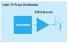
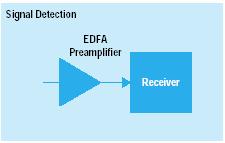
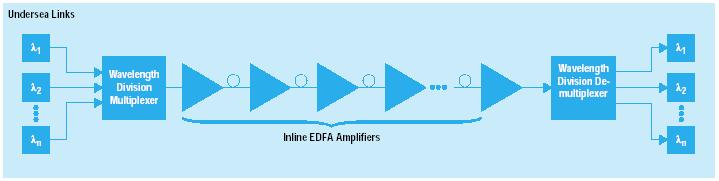
13 Optical Amplifiers - Applications In line amplifier km -To increase transmission link Pre-amplifier -Low noise -To improve receiver sensitivity Booster amplifier - 17 dbm -TV LAN booster amplifier
14 Optical Photodetectors
15 Optical photodetectors (PDs) PDs convert photons to electrons Two photodiode types PIN APD For a photodiode it is reqd that it is sensitive at the used λ small noise long life span small rise-time (large BW, small capacitance) low temperature sensitivity quality/price ratio N η q = N electrons photons

16 PhotoDetectors Basic principle of photodetection Photodetectors made up of S.C materials Photons incident on S.C absorbed by electrons in valence band These electrons acquire higher energy and are excited into the conduction band, leaving behind a hole in the valence band. When an external voltage is applied to the semiconductor, these electron-hole pairs give rise to an electrical current, termed the photocurrent. Principle of quantum mechanics is that each electron can absorb only one photon to transit between energy levels.
17 Photodetection Principle Electron Energy (ev) Photon Electron Hole hv/e Conduction Band E g Valence Band Fig: 3.62 The basic principle of photodetection using a semiconductor. Incident photons are absorbed by electrons in the valence band, creating a free or mobile electron-hole pair. Electron-hole pair gives rise to a photocurrent when an external voltage is applied.
18 Materials commonly used to produce photodiodes: MaterialWavelength range (nm) Silicon Germanium Indium gallium arsenide lead sulfide <
19 PhotoDetectors Energy of the incident photon must be at least equal to the band gap energy in order for a photocurrent to be generated. This gives us the following constraint on the frequency f c or the wavelength λ at which a semiconductor material with band gap E g can be used as a photodetector hf c = hc/λ > ee g The Largest value of λ for which this equation is satisfied is called the cutoff wavelength and is denoted by λ cutoff We see from the table 3.2 that the well-known semiconductors silicon (Si) and gallium arsenide (GaAs) cannot be used in the 1.3 and 1.55 µm bands.
20 PhotoDetectors Although germanium (Ge) can be used in both these bands, it has some disadvantages that reduce its effectiveness for this purpose. New compounds indium gallium arsenide phosphide (InGaAsP) are commonly used to make photodetectors in the 1.3 and 1.55 µm bands. Silicon photodetectors are widely used in the 0.8 µm bands. Fraction of the energy of the optical signal that is absorbed and gives rise to a photocurrent is called the efficiency η of the photodetector. For transmission at high bit rates over long distances, optical energy is scarce, and thus it is important to design the photodetector to achieve an efficiency η as close to 1 as possible. The power absorbed by a semiconductor slab of thickness L μm can be written as P abs = (1- e -άl ) P in Also, η = P abs / P in = 1- e -άl
21 PhotoDetectors Where P in is the incident optical signal power, and α is the absorption coefficient of the material. ά depends on the wavelength and is zero for wavelengths λ > λ cutoff Typical values of α are on the order of 10 4 /cm, so to achieve an efficiency ή > 0.99, a slab of thickness on the order of 10μm is needed. Area of the photodetector is usually chosen to be sufficently large so that all the incident optical power can be captured by it. Photodectectors have very wide operating bandwidth since a photodetector at some wavelength can also serve as a photodetector at all smaller wavelengths. Thus a photodetector designed for the 1.55μm band can also be used in the 1.3μm band.
22 Band gap Energies and Cutoff wavelengths Table 3.2 Material E g (ev) λ cutoff (μm) Si Ge GaAs InP In 0.55 Ga 0.45 As In y Ga 0.45y As y P 1-y
23 PhotoDetectors Photodetectors are commonly characterized by their responsivity R. If a Photodetector produces an average current of I p amperes when the incident optical power is P in watts, then the responsivity is R = I P /P in A/W Since an incident optical power P in corresponds to an incidence of P in /hf c photons/s on the average, and a fraction η of these incident photons are absorbed and generate an electron in the external circuit, we can write R = eη/hfc A/W. Responsivity is commonly expressed in terms of λ; thus R = eηλ / hc = ηλ/1.24 A/W
24 PhotoDetectors Since η can be made quite close to 1 in practice, the responsivities achieved are on the order of 1 A/W in the 1.3µm band 1.2 A/W in the 1.55µm band. Using slab of semiconductor does not give high efficiencies. A photodetector is called a photodiode when a reverse bias voltage is applied to a semiconductor instead of using homogenous slab of it. Depletion region in a pn-junction creates a built-in electric field.
25 PIN Photodiodes To improve the efficiency of the photodetector, a very lightly doped intrinsic semiconductor is introduced between the p- type and n-type semiconductors. Such photodiodes are called pin photodiodes, where the I in PIN is for Intrinsic. Width of the p-type and n-type semiconductors is small compared to the intrinsic region so that much of the light absorption takes place in this region. This increases the efficiency and thus the responsivities of the photodiode. From table 3.2, we see that the cutoff wavelength for InP is 0.92 µm, and that for In GaAs is 1.65 µm. Thus the p-type and n-type regions are transparent in the µm range.
26 PIN Photodiodes PIN diode is a variation on standard pn-diode An intrinsic (pure) layer of semiconductor is fabricated between the p and n-types Depletion layer widens Internal electric field is maintained over a wider layer Because very few electrons and holes are in this region Its resistivity is low Only a small reverse bias is needed to increase the depletion region Stretches almost entire way between the terminals Very fast response times A few nanoseconds or less
27 Front-End Amplifiers Two Front-End amplifier types: High-impedance Amplifier Trans-impedance Amplifier Thermal noise current that arises due to the random motion of electrons and contaminates the photocurrent is inversely proportional to the load resistance. Thus, to minimized the thermal noise, we must make R L large. Thus there is a trade-off between the bandwidth of the photodiode and its noise performance. Thus the transimpedance front end is chosen over the high-impedance one for most optical communication systems.
28 Front-End Amplifiers Photodiode I p R L C + - Amplifier A High-impedance Front End Amplifier Circuit R L Photodiode I p C + - A Amplifier Trans-impedance Front End Amplifier Circuit
29 Front-End Amplifiers There is another consideration in the choice of a frontend amplifier: dynamic range. This is the difference between the largest and smallest signal levels that the front-end amplifier can handle. However, dynamic range of the receivers is very important consideration in the case of networks where the received signal level can vary by a few orders of magnitude, depending on the location of the source in the network. Transimpedance amplifier has significantly higher dynamic range than the high-impedance one, and this is another factor in favor of choosing the transimpedance amplifier.
30 PinFET A field-effect transistor (FET) has very high input impendence and for this reason is often used as the amplifier in the front end. A pin photodiode and an FET are often integrated on the same semiconductor substrate, and the combined device is called pinfet.
Fiberoptic Communication Systems By Dr. M H Zaidi. Optical Amplifiers
 Optical Amplifiers Optical Amplifiers Optical signal propagating in fiber suffers attenuation Optical power level of a signal must be periodically conditioned Optical amplifiers are a key component in
Lecture 18: Photodetectors
 Lecture 18: Photodetectors Contents 1 Introduction 1 2 Photodetector principle 2 3 Photoconductor 4 4 Photodiodes 6 4.1 Heterojunction photodiode.................... 8 4.2 Metal-semiconductor photodiode................
Optical Receivers Theory and Operation
 Optical Receivers Theory and Operation Photo Detectors Optical receivers convert optical signal (light) to electrical signal (current/voltage) Hence referred O/E Converter Photodetector is the fundamental
LEDs, Photodetectors and Solar Cells
 LEDs, Photodetectors and Solar Cells Chapter 7 (Parker) ELEC 424 John Peeples Why the Interest in Photons? Answer: Momentum and Radiation High electrical current density destroys minute polysilicon and
Photodiode: LECTURE-5
 LECTURE-5 Photodiode: Photodiode consists of an intrinsic semiconductor sandwiched between two heavily doped p-type and n-type semiconductors as shown in Fig. 3.2.2. Sufficient reverse voltage is applied
Chapter 12: Optical Amplifiers: Erbium Doped Fiber Amplifiers (EDFAs)
") Chapter 12: Optical Amplifiers: Erbium Doped Fiber Amplifiers (EDFAs) Prof. Dr. Yaocheng SHI ( 时尧成 ) yaocheng@zju.edu.cn http://mypage.zju.edu.cn/yaocheng 1 Traditional Optical Communication System Loss
Chapter 12: Optical Amplifiers: Erbium Doped Fiber Amplifiers (EDFAs) Prof. Dr. Yaocheng SHI ( 时尧成 ) yaocheng@zju.edu.cn http://mypage.zju.edu.cn/yaocheng 1 Traditional Optical Communication System Loss
OFCS OPTICAL DETECTORS 11/9/2014 LECTURES 1
 OFCS OPTICAL DETECTORS 11/9/2014 LECTURES 1 1-Defintion & Mechanisms of photodetection It is a device that converts the incident light into electrical current External photoelectric effect: Electrons are
Detectors for Optical Communications
 Optical Communications: Circuits, Systems and Devices Chapter 3: Optical Devices for Optical Communications lecturer: Dr. Ali Fotowat Ahmady Sep 2012 Sharif University of Technology 1 Photo All detectors
Advanced Optical Communications Prof. R. K. Shevgaonkar Department of Electrical Engineering Indian Institute of Technology, Bombay
 Advanced Optical Communications Prof. R. K. Shevgaonkar Department of Electrical Engineering Indian Institute of Technology, Bombay Lecture No. # 27 EDFA In the last lecture, we talked about wavelength
Optical Amplifiers (Chapter 6)
") Optical Amplifiers (Chapter 6) General optical amplifier theory Semiconductor Optical Amplifier (SOA) Raman Amplifiers Erbium-doped Fiber Amplifiers (EDFA) Read Chapter 6, pp. 226-266 Loss & dispersion
Optical Amplifiers (Chapter 6) General optical amplifier theory Semiconductor Optical Amplifier (SOA) Raman Amplifiers Erbium-doped Fiber Amplifiers (EDFA) Read Chapter 6, pp. 226-266 Loss & dispersion
OPTOELECTRONIC and PHOTOVOLTAIC DEVICES
 OPTOELECTRONIC and PHOTOVOLTAIC DEVICES Outline 1. Introduction to the (semiconductor) physics: energy bands, charge carriers, semiconductors, p-n junction, materials, etc. 2. Light emitting diodes Light
Chap14. Photodiode Detectors
 Chap14. Photodiode Detectors Mohammad Ali Mansouri-Birjandi mansouri@ece.usb.ac.ir mamansouri@yahoo.com Faculty of Electrical and Computer Engineering University of Sistan and Baluchestan (USB) Design
Chapter 3 OPTICAL SOURCES AND DETECTORS
 Chapter 3 OPTICAL SOURCES AND DETECTORS 3. Optical sources and Detectors 3.1 Introduction: The success of light wave communications and optical fiber sensors is due to the result of two technological breakthroughs.
FIBER OPTICS. Prof. R.K. Shevgaonkar. Department of Electrical Engineering. Indian Institute of Technology, Bombay. Lecture: 20
 FIBER OPTICS Prof. R.K. Shevgaonkar Department of Electrical Engineering Indian Institute of Technology, Bombay Lecture: 20 Photo-Detectors and Detector Noise Fiber Optics, Prof. R.K. Shevgaonkar, Dept.
Optical Amplifiers Photonics and Integrated Optics (ELEC-E3240) Zhipei Sun Photonics Group Department of Micro- and Nanosciences Aalto University
 Zhipei Sun Photonics Group Department of Micro- and Nanosciences Aalto University") Photonics Group Department of Micro- and Nanosciences Aalto University Optical Amplifiers Photonics and Integrated Optics (ELEC-E3240) Zhipei Sun Last Lecture Topics Course introduction Ray optics & optical
Photonics Group Department of Micro- and Nanosciences Aalto University Optical Amplifiers Photonics and Integrated Optics (ELEC-E3240) Zhipei Sun Last Lecture Topics Course introduction Ray optics & optical
Downloaded from
 Question 14.1: In an n-type silicon, which of the following statement is true: (a) Electrons are majority carriers and trivalent atoms are the dopants. (b) Electrons are minority carriers and pentavalent
Examination Optoelectronic Communication Technology. April 11, Name: Student ID number: OCT1 1: OCT 2: OCT 3: OCT 4: Total: Grade:
 Examination Optoelectronic Communication Technology April, 26 Name: Student ID number: OCT : OCT 2: OCT 3: OCT 4: Total: Grade: Declaration of Consent I hereby agree to have my exam results published on
Introduction Fundamental of optical amplifiers Types of optical amplifiers
 ECE 6323 Introduction Fundamental of optical amplifiers Types of optical amplifiers Erbium-doped fiber amplifiers Semiconductor optical amplifier Others: stimulated Raman, optical parametric Advanced application:
S Optical Networks Course Lecture 2: Essential Building Blocks
 S-72.3340 Optical Networks Course Lecture 2: Essential Building Blocks Edward Mutafungwa Communications Laboratory, Helsinki University of Technology, P. O. Box 2300, FIN-02015 TKK, Finland Tel: +358 9
Optodevice Data Book ODE I. Rev.9 Mar Opnext Japan, Inc.
 Optodevice Data Book ODE-408-001I Rev.9 Mar. 2003 Opnext Japan, Inc. Section 1 Operating Principles 1.1 Operating Principles of Laser Diodes (LDs) and Infrared Emitting Diodes (IREDs) 1.1.1 Emitting Principles
Electron Devices and Circuits (EC 8353)
") Electron Devices and Circuits (EC 8353) Prepared by Ms.S.KARKUZHALI, A.P/EEE Diodes The diode is a 2-terminal device. A diode ideally conducts in only one direction. Diode Characteristics Conduction Region
Electron Devices and Circuits (EC 8353) Prepared by Ms.S.KARKUZHALI, A.P/EEE Diodes The diode is a 2-terminal device. A diode ideally conducts in only one direction. Diode Characteristics Conduction Region
OPTI510R: Photonics. Khanh Kieu College of Optical Sciences, University of Arizona Meinel building R.626
 OPTI510R: Photonics Khanh Kieu College of Optical Sciences, University of Arizona kkieu@optics.arizona.edu Meinel building R.626 Photodetectors Introduction Most important characteristics Photodetector
InP-based Waveguide Photodetector with Integrated Photon Multiplication
 InP-based Waveguide Photodetector with Integrated Photon Multiplication D.Pasquariello,J.Piprek,D.Lasaosa,andJ.E.Bowers Electrical and Computer Engineering Department University of California, Santa Barbara,
ECE 340 Lecture 29 : LEDs and Lasers Class Outline:
 ECE 340 Lecture 29 : LEDs and Lasers Class Outline: Light Emitting Diodes Lasers Semiconductor Lasers Things you should know when you leave Key Questions What is an LED and how does it work? How does a
UNIT III. By Ajay Kumar Gautam Asst. Prof. Electronics & Communication Engineering Dev Bhoomi Institute of Technology & Engineering, Dehradun
 UNIT III By Ajay Kumar Gautam Asst. Prof. Electronics & Communication Engineering Dev Bhoomi Institute of Technology & Engineering, Dehradun SYLLABUS Optical Absorption in semiconductors, Types of Photo
Downloaded from
 SOLID AND SEMICONDUCTOR DEVICES (EASY AND SCORING TOPIC) 1. Distinction of metals, semiconductor and insulator on the basis of Energy band of Solids. 2. Types of Semiconductor. 3. PN Junction formation
Key Questions. What is an LED and how does it work? How does a laser work? How does a semiconductor laser work? ECE 340 Lecture 29 : LEDs and Lasers
 Things you should know when you leave Key Questions ECE 340 Lecture 29 : LEDs and Class Outline: What is an LED and how does it How does a laser How does a semiconductor laser How do light emitting diodes
Optical Fiber Communication Lecture 11 Detectors
 Optical Fiber Communication Lecture 11 Detectors Warriors of the Net Detector Technologies MSM (Metal Semiconductor Metal) PIN Layer Structure Semiinsulating GaAs Contact InGaAsP p 5x10 18 Absorption InGaAs
Lecture 9 External Modulators and Detectors
 Optical Fibres and Telecommunications Lecture 9 External Modulators and Detectors Introduction Where are we? A look at some real laser diodes. External modulators Mach-Zender Electro-absorption modulators
Physics of Waveguide Photodetectors with Integrated Amplification
 Physics of Waveguide Photodetectors with Integrated Amplification J. Piprek, D. Lasaosa, D. Pasquariello, and J. E. Bowers Electrical and Computer Engineering Department University of California, Santa
Semiconductor Optoelectronics Prof. M. R. Shenoy Department of Physics Indian Institute of Technology, Delhi
 Semiconductor Optoelectronics Prof. M. R. Shenoy Department of Physics Indian Institute of Technology, Delhi Lecture - 26 Semiconductor Optical Amplifier (SOA) (Refer Slide Time: 00:39) Welcome to this
Avalanche Photodiode. Instructor: Prof. Dietmar Knipp Presentation by Peter Egyinam. 4/19/2005 Photonics and Optical communicaton
 Avalanche Photodiode Instructor: Prof. Dietmar Knipp Presentation by Peter Egyinam 1 Outline Background of Photodiodes General Purpose of Photodiodes Basic operation of p-n, p-i-n and avalanche photodiodes
Investigate the characteristics of PIN Photodiodes and understand the usage of the Lightwave Analyzer component.
 PIN Photodiode 1 OBJECTIVE Investigate the characteristics of PIN Photodiodes and understand the usage of the Lightwave Analyzer component. 2 PRE-LAB In a similar way photons can be generated in a semiconductor,
Lecture 6 Fiber Optical Communication Lecture 6, Slide 1
 Lecture 6 Optical transmitters Photon processes in light matter interaction Lasers Lasing conditions The rate equations CW operation Modulation response Noise Light emitting diodes (LED) Power Modulation
UNIT-III SOURCES AND DETECTORS. According to the shape of the band gap as a function of the momentum, semiconductors are classified as
 UNIT-III SOURCES AND DETECTORS DIRECT AND INDIRECT BAND GAP SEMICONDUCTORS: According to the shape of the band gap as a function of the momentum, semiconductors are classified as 1. Direct band gap semiconductors
Fundamentals of CMOS Image Sensors
 CHAPTER 2 Fundamentals of CMOS Image Sensors Mixed-Signal IC Design for Image Sensor 2-1 Outline Photoelectric Effect Photodetectors CMOS Image Sensor(CIS) Array Architecture CIS Peripherals Design Considerations
Lecture 14: Photodiodes
 Lecture 14: Photodiodes Background concepts p-n photodiodes photoconductive/photovoltaic modes p-i-n photodiodes responsivity and bandwidth Reading: Senior 8.1-8.8.3 Keiser Chapter 6 1 Electron-hole photogeneration
Figure Responsivity (A/W) Figure E E-09.
 Figure E E-09.") OSI Optoelectronics, is a leading manufacturer of fiber optic components for communication systems. The products offer range for Silicon, GaAs and InGaAs to full turnkey solutions. Photodiodes are semiconductor
OSI Optoelectronics, is a leading manufacturer of fiber optic components for communication systems. The products offer range for Silicon, GaAs and InGaAs to full turnkey solutions. Photodiodes are semiconductor
Chapter 1: Semiconductor Diodes
 Chapter 1: Semiconductor Diodes Diodes The diode is a 2-terminal device. A diode ideally conducts in only one direction. 2 Diode Characteristics Conduction Region Non-Conduction Region The voltage across
Fundamentals of Laser
 SMR 1826-3 Preparatory School to the Winter College on Fibre 5-9 February 2007 Fundamentals of Laser Imrana Ashraf Zahid Quaid-i-Azam University Islamabad Pakistan Fundamentals of Laser Dr. Imrana Ashraf
Figure Figure E E-09. Dark Current (A) 1.
 1.") OSI Optoelectronics, is a leading manufacturer of fiber optic components for communication systems. The products offer range for Silicon, GaAs and InGaAs to full turnkey solutions. Photodiodes are semiconductor
OSI Optoelectronics, is a leading manufacturer of fiber optic components for communication systems. The products offer range for Silicon, GaAs and InGaAs to full turnkey solutions. Photodiodes are semiconductor
Luminous Equivalent of Radiation
 Intensity vs λ Luminous Equivalent of Radiation When the spectral power (p(λ) for GaP-ZnO diode has a peak at 0.69µm) is combined with the eye-sensitivity curve a peak response at 0.65µm is obtained with
UNIT IX ELECTRONIC DEVICES
 UNT X ELECTRONC DECES Weightage Marks : 07 Semiconductors Semiconductors diode-- characteristics in forward and reverse bias, diode as rectifier. - characteristics of LED, Photodiodes, solarcell and Zener
Chapter 8. Wavelength-Division Multiplexing (WDM) Part II: Amplifiers
 Part II: Amplifiers") Chapter 8 Wavelength-Division Multiplexing (WDM) Part II: Amplifiers Introduction Traditionally, when setting up an optical link, one formulates a power budget and adds repeaters when the path loss exceeds
Chapter 8 Wavelength-Division Multiplexing (WDM) Part II: Amplifiers Introduction Traditionally, when setting up an optical link, one formulates a power budget and adds repeaters when the path loss exceeds
Basic concepts. Optical Sources (b) Optical Sources (a) Requirements for light sources (b) Requirements for light sources (a)
 Optical Sources (a) Requirements for light sources (b) Requirements for light sources (a)") Optical Sources (a) Optical Sources (b) The main light sources used with fibre optic systems are: Light-emitting diodes (LEDs) Semiconductor lasers (diode lasers) Fibre laser and other compact solid-state
Optical Sources (a) Optical Sources (b) The main light sources used with fibre optic systems are: Light-emitting diodes (LEDs) Semiconductor lasers (diode lasers) Fibre laser and other compact solid-state
Optical Communications
 Optical Communications Telecommunication Engineering School of Engineering University of Rome La Sapienza Rome, Italy 2005-2006 Lecture #4, May 9 2006 Receivers OVERVIEW Photodetector types: Photodiodes
Optical Fibre Amplifiers Continued
 1 Optical Fibre Amplifiers Continued Stavros Iezekiel Department of Electrical and Computer Engineering University of Cyprus ECE 445 Lecture 09 Fall Semester 2016 2 ERBIUM-DOPED FIBRE AMPLIFIERS BASIC
Optical Fiber Amplifiers. Scott Freese. Physics May 2008
 Optical Fiber Amplifiers Scott Freese Physics 262 2 May 2008 Partner: Jared Maxson Abstract The primary goal of this experiment was to gain an understanding of the basic components of an Erbium doped fiber
Department of Electrical Engineering IIT Madras
 Department of Electrical Engineering IIT Madras Sample Questions on Semiconductor Devices EE3 applicants who are interested to pursue their research in microelectronics devices area (fabrication and/or
Lecture 4 Fiber Optical Communication Lecture 4, Slide 1
 Lecture 4 Optical transmitters Photon processes in light matter interaction Lasers Lasing conditions The rate equations CW operation Modulation response Noise Light emitting diodes (LED) Power Modulation
Chapter Semiconductor Electronics
 Chapter Semiconductor Electronics Q1. p-n junction is said to be forward biased, when [1988] (a) the positive pole of the battery is joined to the p- semiconductor and negative pole to the n- semiconductor
Recent Development and Study of Silicon Solid State Photomultiplier (MRS Avalanche Photodetector)
") Recent Development and Study of Silicon Solid State Photomultiplier (MRS Avalanche Photodetector) Valeri Saveliev University of Obninsk, Russia Vienna Conference on Instrumentation Vienna, 20 February
Recent Development and Study of Silicon Solid State Photomultiplier (MRS Avalanche Photodetector) Valeri Saveliev University of Obninsk, Russia Vienna Conference on Instrumentation Vienna, 20 February
InP-based Waveguide Photodetector with Integrated Photon Multiplication
 InP-based Waveguide Photodetector with Integrated Photon Multiplication D.Pasquariello,J.Piprek,D.Lasaosa,andJ.E.Bowers Electrical and Computer Engineering Department University of California, Santa Barbara,
Comparative Study of an Optical Link with PIN and APD as Photo-Detector Preetam Jain 1, Dr Lochan Jolly 2
 Comparative Study of an Optical Link with PIN and APD as Photo-Detector Preetam Jain 1, Dr Lochan Jolly 2 1 ME EXTC Student Thakur College of Engineering and Technology 2 Professor Thakur College of Engineering
 Energy band diagrams Metals: 9. ELECTRONIC DEVICES GIST ρ= 10-2 to 10-8 Ω m Insulators: ρ> 10 8 Ω m Semiconductors ρ= 1 to 10 5 Ω m 109 A. Intrinsic semiconductors At T=0k it acts as insulator At room
UNIT - 5 OPTICAL RECEIVER
 UNIT - 5 LECTURE-1 OPTICAL RECEIVER Introduction, Optical Receiver Operation, receiver sensitivity, quantum limit, eye diagrams, coherent detection, burst mode receiver operation, Analog receivers. RECOMMENDED
MAHALAKSHMI ENGINEERING COLLEGE TIRUCHIRAPALLI
 MAHALAKSHMI ENGINEERING COLLEGE TIRUCHIRAPALLI - 621213 DEPARTMENT : ECE SUBJECT NAME : OPTICAL COMMUNICATION & NETWORKS SUBJECT CODE : EC 2402 UNIT III: SOURCES AND DETECTORS PART -A (2 Marks) 1. What
Absorption: in an OF, the loss of Optical power, resulting from conversion of that power into heat.
 Absorption: in an OF, the loss of Optical power, resulting from conversion of that power into heat. Scattering: The changes in direction of light confined within an OF, occurring due to imperfection in
What is the highest efficiency Solar Cell?
 What is the highest efficiency Solar Cell? GT CRC Roof-Mounted PV System Largest single PV structure at the time of it s construction for the 1996 Olympic games Produced more than 1 billion watt hrs. of
Light Sources, Modulation, Transmitters and Receivers
 Optical Fibres and Telecommunications Light Sources, Modulation, Transmitters and Receivers Introduction Previous section looked at Fibres. How is light generated in the first place? How is light modulated?
Electronic devices-i. Difference between conductors, insulators and semiconductors
 Electronic devices-i Semiconductor Devices is one of the important and easy units in class XII CBSE Physics syllabus. It is easy to understand and learn. Generally the questions asked are simple. The unit
Università degli Studi di Roma Tor Vergata Dipartimento di Ingegneria Elettronica. Analogue Electronics. Paolo Colantonio A.A.
 Università degli Studi di Roma Tor Vergata Dipartimento di Ingegneria Elettronica Analogue Electronics Paolo Colantonio A.A. 2015-16 Introduction: materials Conductors e.g. copper or aluminum have a cloud
Optical Communications and Networking 朱祖勍. Oct. 9, 2017
 Optical Communications and Networking Oct. 9, 2017 1 Optical Amplifiers In optical communication systems, the optical signal from the transmitter are attenuated by the fiber and other passive components
 Electronic Devices 1. Current flowing in each of the following circuits A and respectively are: (Circuit 1) (Circuit 2) 1) 1A, 2A 2) 2A, 1A 3) 4A, 2A 4) 2A, 4A 2. Among the following one statement is not
CONTENTS. 2.2 Schrodinger's Wave Equation 31. PART I Semiconductor Material Properties. 2.3 Applications of Schrodinger's Wave Equation 34
 CONTENTS Preface x Prologue Semiconductors and the Integrated Circuit xvii PART I Semiconductor Material Properties CHAPTER 1 The Crystal Structure of Solids 1 1.0 Preview 1 1.1 Semiconductor Materials
Key Questions ECE 340 Lecture 28 : Photodiodes
 Things you should know when you leave Key Questions ECE 340 Lecture 28 : Photodiodes Class Outline: How do the I-V characteristics change with illumination? How do solar cells operate? How do photodiodes
Low threshold continuous wave Raman silicon laser
 NATURE PHOTONICS, VOL. 1, APRIL, 2007 Low threshold continuous wave Raman silicon laser HAISHENG RONG 1 *, SHENGBO XU 1, YING-HAO KUO 1, VANESSA SIH 1, ODED COHEN 2, OMRI RADAY 2 AND MARIO PANICCIA 1 1:
Design and Simulation of N-Substrate Reverse Type Ingaasp/Inp Avalanche Photodiode
 International Refereed Journal of Engineering and Science (IRJES) ISSN (Online) 2319-183X, (Print) 2319-1821 Volume 2, Issue 8 (August 2013), PP.34-39 Design and Simulation of N-Substrate Reverse Type
Functional Materials. Optoelectronic devices
 Functional Materials Lecture 2: Optoelectronic materials and devices (inorganic). Photonic materials Optoelectronic devices Light-emitting diode (LED) displays Photodiode and Solar cell Photoconductive
International Journal of Research in Advent Technology Available Online at:
 MODELLING LIGHT EMITTING DIODE USING SPICE Dattaprasad Madur 1, Najib Ghatte 2, init Pereira 3, Tushar Surwadkar 4 1 2 3 4 Department of Electronics Fr. Conceicao Rodrigues College of Engineering Fr. Agnel
EDFA SIMULINK MODEL FOR ANALYZING GAIN SPECTRUM AND ASE. Stephen Z. Pinter
 EDFA SIMULINK MODEL FOR ANALYZING GAIN SPECTRUM AND ASE Stephen Z. Pinter Ryerson University Department of Electrical and Computer Engineering spinter@ee.ryerson.ca December, 2003 ABSTRACT A Simulink model
Review of Semiconductor Physics
 Review of Semiconductor Physics k B 1.38 u 10 23 JK -1 a) Energy level diagrams showing the excitation of an electron from the valence band to the conduction band. The resultant free electron can freely
Optical MEMS in Compound Semiconductors Advanced Engineering Materials, Cal Poly, SLO November 16, 2007
 Optical MEMS in Compound Semiconductors Advanced Engineering Materials, Cal Poly, SLO November 16, 2007 Outline Brief Motivation Optical Processes in Semiconductors Reflectors and Optical Cavities Diode
Study and Measurement of the Main Parameters of a Laser quadrant Detector
 Cairo University National Institute of Laser Enhanced Sciences Laser Sciences and Interactions Study and Measurement of the Main Parameters of a Laser quadrant Detector By Eng. Mohamed Abd-Elfattah Abd-Elazim
Electronics The basics of semiconductor physics
 Electronics The basics of semiconductor physics Prof. Márta Rencz, Gábor Takács BME DED 17/09/2015 1 / 37 The basic properties of semiconductors Range of conductivity [Source: http://www.britannica.com]
Optical Sources and Detectors
 Optical Sources and Detectors 1. Optical Sources Optical transmitter coverts electrical input signal into corresponding optical signal. The optical signal is then launched into the fiber. Optical source
Problem 4 Consider a GaAs p-n + junction LED with the following parameters at 300 K: Electron diusion coecient, D n = 25 cm 2 =s Hole diusion coecient
 Prof. Jasprit Singh Fall 2001 EECS 320 Homework 7 This homework is due on November 8. Problem 1 An optical power density of 1W/cm 2 is incident on a GaAs sample. The photon energy is 2.0 ev and there is
Solar Cell Parameters and Equivalent Circuit
 9 Solar Cell Parameters and Equivalent Circuit 9.1 External solar cell parameters The main parameters that are used to characterise the performance of solar cells are the peak power P max, the short-circuit
is a method of transmitting information from one place to another by sending light through an optical fiber. The light forms an electromagnetic
 is a method of transmitting information from one place to another by sending light through an optical fiber. The light forms an electromagnetic carrier wave that is modulated to carry information. The
Module 04.(B1) Electronic Fundamentals
 Electronic Fundamentals") 1.1a. Semiconductors - Diodes. Module 04.(B1) Electronic Fundamentals Question Number. 1. What gives the colour of an LED?. Option A. The active element. Option B. The plastic it is encased in. Option
1.1a. Semiconductors - Diodes. Module 04.(B1) Electronic Fundamentals Question Number. 1. What gives the colour of an LED?. Option A. The active element. Option B. The plastic it is encased in. Option
LED lecture. Wei Chih Wang University of Washington
 LED lecture Wei Chih Wang University of Washington Linear and Nonlinear electronics current voltage Vaccum tube (i.e. type 2A3) voltage Thermistor (large negative temperature coefficient of resistivity)
SRM INSTITUTE OF SCIENCE AND TECHNOLOGY (DEEMED UNIVERSITY)
") SRM INSTITUTE OF SCIENCE AND TECHNOLOGY (DEEMED UNIVERSITY) QUESTION BANK I YEAR B.Tech (II Semester) ELECTRONIC DEVICES (COMMON FOR EC102, EE104, IC108, BM106) UNIT-I PART-A 1. What are intrinsic and
SRM INSTITUTE OF SCIENCE AND TECHNOLOGY (DEEMED UNIVERSITY) QUESTION BANK I YEAR B.Tech (II Semester) ELECTRONIC DEVICES (COMMON FOR EC102, EE104, IC108, BM106) UNIT-I PART-A 1. What are intrinsic and
PHYSICAL ELECTRONICS(ECE3540) APPLICATIONS OF PHYSICAL ELECTRONICS PART I
 APPLICATIONS OF PHYSICAL ELECTRONICS PART I") PHYSICAL ELECTRONICS(ECE3540) APPLICATIONS OF PHYSICAL ELECTRONICS PART I Tennessee Technological University Monday, October 28, 2013 1 Introduction In the following slides, we will discuss the summary
PHYSICAL ELECTRONICS(ECE3540) APPLICATIONS OF PHYSICAL ELECTRONICS PART I Tennessee Technological University Monday, October 28, 2013 1 Introduction In the following slides, we will discuss the summary
Electronic Circuits I. Instructor: Dr. Alaa Mahmoud
 Electronic Circuits I Instructor: Dr. Alaa Mahmoud alaa_y_emam@hotmail.com Chapter 27 Diode and diode application Outline: Semiconductor Materials The P-N Junction Diode Biasing P-N Junction Volt-Ampere
DESIGN TEMPLATE ISSUES ANALYSIS FOR ROBUST DESIGN OUTPUT. performance, yield, reliability
 DESIGN TEMPLATE ISSUES performance, yield, reliability ANALYSIS FOR ROBUST DESIGN properties, figure-of-merit thermodynamics, kinetics, process margins process control OUTPUT models, options Optical Amplification
Photonics and Optical Communication Spring 2005
 Photonics and Optical Communication Spring 2005 Final Exam Instructor: Dr. Dietmar Knipp, Assistant Professor of Electrical Engineering Name: Mat. -Nr.: Guidelines: Duration of the Final Exam: 2 hour You
Module 10 - Optical Amplifiers
 Module 10 - Optical Amplifiers Dr. Alan Kost Associate Research Professor Of Optical Sciences, University Of Arizona Dr. Alan Kost is an Associate Research Professor of Optical Sciences in the University
Chapter 14 Semiconductor Electronics Materials Devices And Simple Circuits
 Class XII Chapter 14 Semiconductor Electronics Materials Devices And Simple Circuits Physics Question 14.1: In an n-type silicon, which of the following statement is true: (a) Electrons are majority carriers
Components of Optical Instruments. Chapter 7_III UV, Visible and IR Instruments
 Components of Optical Instruments Chapter 7_III UV, Visible and IR Instruments 1 Grating Monochromators Principle of operation: Diffraction Diffraction sources: grooves on a reflecting surface Fabrication:
Reg. No. : Question Paper Code : B.E./B.Tech. DEGREE EXAMINATION, NOVEMBER/DECEMBER Second Semester
 WK 5 Reg. No. : Question Paper Code : 27184 B.E./B.Tech. DEGREE EXAMINATION, NOVEMBER/DECEMBER 2015. Time : Three hours Second Semester Electronics and Communication Engineering EC 6201 ELECTRONIC DEVICES
The Report of Gain Performance Characteristics of the Erbium Doped Fiber Amplifier (EDFA)
") The Report of Gain Performance Characteristics of the Erbium Doped Fiber Amplifier (EDFA) Masruri Masruri (186520) 22/05/2008 1 Laboratory Setup The laboratory setup using in this laboratory experiment
The Report of Gain Performance Characteristics of the Erbium Doped Fiber Amplifier (EDFA) Masruri Masruri (186520) 22/05/2008 1 Laboratory Setup The laboratory setup using in this laboratory experiment
Digital Electronics. By: FARHAD FARADJI, Ph.D. Assistant Professor, Electrical and Computer Engineering, K. N. Toosi University of Technology
 K. N. Toosi University of Technology Chapter 7. Field-Effect Transistors By: FARHAD FARADJI, Ph.D. Assistant Professor, Electrical and Computer Engineering, K. N. Toosi University of Technology http://wp.kntu.ac.ir/faradji/digitalelectronics.htm
Opto-electronic Receivers
 Purpose of a Receiver The receiver fulfils the function of optoelectronic conversion of an input optical signal into an output electrical signal (data stream). The purpose is to recover the data transmitted
Semiconductor Optical Communication Components and Devices Lecture 18: Introduction to Diode Lasers - I
 Semiconductor Optical Communication Components and Devices Lecture 18: Introduction to Diode Lasers - I Prof. Utpal Das Professor, Department of lectrical ngineering, Laser Technology Program, Indian Institute
UNIT 3 Transistors JFET
 UNIT 3 Transistors JFET Mosfet Definition of BJT A bipolar junction transistor is a three terminal semiconductor device consisting of two p-n junctions which is able to amplify or magnify a signal. It
EE70 - Intro. Electronics
 EE70 - Intro. Electronics Course website: ~/classes/ee70/fall05 Today s class agenda (November 28, 2005) review Serial/parallel resonant circuits Diode Field Effect Transistor (FET) f 0 = Qs = Qs = 1 2π
Introduction Fundamentals of laser Types of lasers Semiconductor lasers
 ECE 5368 Introduction Fundamentals of laser Types of lasers Semiconductor lasers Introduction Fundamentals of laser Types of lasers Semiconductor lasers How many types of lasers? Many many depending on
for optical communication system
 High speed Ge waveguide detector for optical communication system Xingjun Wang, Zhijuan Tu and Zhiping Zhou State Key Laboratory of Advanced Optical Communication Systems and Networks, School of Electronics
Unit 2 Semiconductor Devices. Lecture_2.5 Opto-Electronic Devices
 Unit 2 Semiconductor Devices Lecture_2.5 Opto-Electronic Devices Opto-electronics Opto-electronics is the study and application of electronic devices that interact with light. Electronics (electrons) Optics
OPTI510R: Photonics. Khanh Kieu College of Optical Sciences, University of Arizona Meinel building R.626
 OPTI510R: Photonics Khanh Kieu College of Optical Sciences, University of Arizona kkieu@optics.arizona.edu Meinel building R.626 Announcements HW #5 is assigned (due April 9) April 9 th class will be in