LED lecture. Wei Chih Wang University of Washington
|
|
|
- Hope Robertson
- 5 years ago
- Views:
Transcription
1 LED lecture Wei Chih Wang University of Washington
2 Linear and Nonlinear electronics current voltage Vaccum tube (i.e. type 2A3) voltage Thermistor (large negative temperature coefficient of resistivity) voltage Diode (i.e. PN diode, LED, laser diode, phtodiode) i D v D I nv T S e 1 current voltage Normal resistor Ohm s Law: i=v/r
3 Introduction to Diodes ANODE D1 DIODE CATHODE A diode can be considered to be an electrical one way valve. They are made from a large variety of materials including silicon, germanium, gallium arsenide, silicon carbide


4 Introduction to Diodes In effect, diodes act like a flapper valve Note: this is the simplest possible model of a diode
5 Introduction to Diodes For the flapper valve, a small positive pressure is required to open. Likewise, for a diode, a small positive voltage is required to turn it on. This voltage is like the voltage required to power some electrical device. It is used up turning the device on so the voltages at the two ends of the diode will differ. The voltage required to turn on a diode is typically around volt for a standard silicon diode and a few volts for a light emitting diode (LED)
6 Introduction to Diodes 1 0 V 5 V 0 V - 5 V V 0 s 0. 5 m s 1. 0 m s 1. 5 m s 2. 0 m s 2. 5 m s 3. 0 m s 10 volt sinusoidal voltage source T i m e V ( D 1 : 1 ) D1 VAMPL = 10V FREQ = 1k V1 D1N4002 R1 1k Connect to a resistive load through a diode 0
7 Introduction to Diodes D1 VAMPL = 10V FREQ = 1k V1 V D1N4002 V R1 1k Only positive current flows 0 0.7V 10V 5V 0V -5V -10V 0s 0.5ms 1.0ms 1.5ms 2.0ms 2.5ms 3.0ms V(D1:1) V(D1:2) Time
8 Semiconductor Variable conductivity A pure semiconductor is a poor electrical conductor as a consequence of having just the right number of electrons to completely fill its valence bonds. Through various techniques (e.g., doping or gating), the semiconductor can be modified to have excess of electrons (becoming an n-type semiconductor) or a deficiency of electrons (becoming a p-type semiconductor). In both cases, the semiconductor becomes much more conductive (the conductivity can be increased by a factor of one million, or even more). Semiconductor devices exploit this effect to shape electrical current. Junctions When doped semiconductors are joined to metals, to different semiconductors, and to the same semiconductor with different doping, the resulting junction often strips the electron excess or deficiency out from the semiconductor near the junction. This depletion region is rectifying (only allowing current to flow in one direction), and used to further shape electrical currents in semiconductor devices. Energetic electrons travel far Electrons can be excited across the energy band gap (see Physics below) of a semiconductor by various means. These electrons can carry their excess energy over distance scales of microns before dissipating their energy into heat, significantly longer than is possible in metals. This effect is essential to the operation of bipolar junction transistors. Light energy conversion Electrons in a semiconductor can absorb light, and subsequently retain the energy from the light for a long enough time to be useful for producing electrical work instead of heat. This principle is used in the photovoltaic cell. Conversely, in certain semiconductors, electrically excited electrons can relax by emitting light instead of producing heat. This is used in the light emitting diode. Thermal energy conversion Semiconductors are good materials for thermoelectric coolers and thermoelectric generators, which convert temperature differences into electrical power and vice versa. Peltier coolers use semiconductors for this reason.
9 P type and N type Materials The semiconductor can be modified to have excess of electrons (becoming an n-type semiconductor) or a deficiency of electrons (becoming a p-type semiconductor). In both cases, the semiconductor becomes much more conductive (the conductivity can be increased by a factor of one million, or even more). Semiconductor devices exploit this effect to shape electrical current.
, having four valence electrons, needs to be doped as an n-type semiconductor, elements from group V like phosphorus (P) or arsenic (As) can be used because they have")

10 Donor ( n type semiconductors) In semiconductor physics, a donor is a dopant atom that, when added to a semiconductor, can form a n-type region. For example, when silicon (Si), having four valence electrons, needs to be doped as an n-type semiconductor, elements from group V like phosphorus (P) or arsenic (As) can be used because they have five valence electrons. A dopant with five valence electrons is also called a pentavalent impurity. Other pentavalent dopants are antimony (Sb) and bismuth (Bi). When substituting a Si atom in the crystal lattice, four of the valence electrons of phosphorus form covalent bonds with the neighbouring Si atoms but the fifth one remains weakly bonded. At room temperature, all the fifth electrons are liberated, can move around the Si crystal and can carry a current and thus act as charge carriers. The initially neutral donor becomes positively charged (ionised).
, having four valence electrons, needs to be doped as a p type semiconductor, elements from group III like boron (B) or aluminium (Al), having three valence electrons,")
11 Acceptor (P type semiconductors) In semiconductor physics, an acceptor is a dopant atom that when added to a semiconductor can form a p type region. For example, when silicon (Si), having four valence electrons, needs to be doped as a p type semiconductor, elements from group III like boron (B) or aluminium (Al), having three valence electrons, can be used. The latter elements are also called trivalent impurities. Other trivalent dopants include indium (In) and gallium (Ga). When substituting a Si atom in the crystal lattice, the three valence electrons of boron form covalent bonds with three of the Si neighbours but the bond with the fourth neighbour remains unsatisfied. The unsatisfied bond attracts electrons from the neighbouring bonds. At room temperature, an electron from the neighbouring bond will jump to repair the unsatisfied bond thus leaving a hole (a place where an electron is deficient). The hole will again attract an electron from the neighbouring bond to repair this unsatisfied bond. This chain like process results in the hole moving around the crystal and able to carry a current thus acting as a charge carrier. The initially electroneutral acceptor becomes negatively charged (ionised).
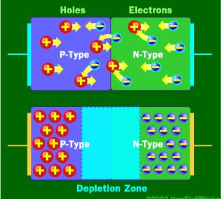
12 How Diodes Work When put two materials together, free electrons from the N-type material fill holes from the P-type material. This creates an insulating layer in the middle of the diode called the depletion zone.
13 How Diodes Work ANODE D1 DIODE CATHODE
14 How Diodes Work ANODE D1 DIODE CATHODE When the positive end of the battery is hooked up to the N-type layer and the negative end is hooked up to the P-type layer, free electrons collect on one end of the diode and holes collect on the other. The depletion zone gets bigger and no current flows.
15 Introduction to Diodes D1 VAMPL = 10V FREQ = 1k V1 V D1N4002 V R1 1k Only positive current flows 0 10V 5V 0V -5V -10V 0s 0.5ms 1.0ms 1.5ms 2.0ms 2.5ms 3.0ms V(D1:1) V(D1:2) Time
16 Part A: Diode i v Characteristic Curves What is a i v characteristic curve? i v curve of an ideal diode i v curve of a real diode
17 What is an i v characteristic curve? Recall that the i v relationship for a resistor is given by Ohm s Law: i=v/r If we plot the voltage across the resistor vs. the current through the resistor, we obtain i v The slope of the straight line is given by 1/R
18 What is an i v characteristic curve? If we change the axis variables, we can obtain i v characteristic curves. R V V1 R2 1k 0 10mA 5mA V-I Characteristic of a 500 Ohm Resistor 0A -5mA -10mA -6.0V -4.0V -2.0V 0V 2.0V 4.0V 6.0V I(R1) V(R1:1) - V(R1:2)
19 i v characteristic for an ideal diode i D Ideal Diode When voltage across the diode is negative, the diode looks like an open circuit. 0 When voltage across the diode is positive, the diode looks like a short. v D

20 i v characteristic of a real diode Real diode is close to ideal Ideal Diode i D v D I nv T S e 1

21 How Diodes Work ANODE D1 DIODE CATHODE
22 How Diodes Work ANODE D1 DIODE CATHODE When the positive end of the battery is hooked up to the N-type layer and the negative end is hooked up to the P-type layer, free electrons collect on one end of the diode and holes collect on the other. The depletion zone gets bigger and no current flows.
23 Real diode characteristics A very large current can flow when the diode is forward biased. For power diodes, currents of a few amps can flow with bias voltages of 0.6 to 1.5V. Note that the textbook generally uses 0.6V as the standard value, but 0.7V is more typical for the devices. Reverse breakdown voltages can be as low as 50V and as large as 1000V. Reverse saturation currents I s are typically 1nA or less.
24 The diode equation The i D v D relationship (without breakdown) can be written simply as: i D v D I nv T S e 1 v D is the voltage across the diode and i D is the current through the diode. n and I s are constants. V T is a voltage proportional to the temperature, we use V. Note that for v D less than zero, the exponential term vanishes and the current i D is roughly equal to minus the saturation current. For v D greater than zero, the current increases exponentially.
25 R1 Diode equation 5V V2 1k D1 D1N m 0 16m 12m 0 exponential term takes over < 0 exponential terms << 1 so Is takes over 8m 4m i D v D I nv T S e 1 i D 0-16V -14V -12V -10V -8V -6V -4V -2V 0V 2V Both the simulated current vs. voltage (green) and the characteristic equation (red) for the diode are plotted.
. Infrared LEDs emit in one of several bands just beyond red light.")
26 Light Emitting Diodes The Light Emitting Diode (LED) is a semiconductor pn junction diode that emits visible light or nearinfrared radiation when forward biased. Visible LEDs emit relatively narrow bands of green, yellow, orange, or red light (tens of nm). Infrared LEDs emit in one of several bands just beyond red light.
27 Facts about LEDs LEDs switch off and on rapidly, are very rugged and efficient, have a very long lifetime, and are easy to use (~ns to s). They are current dependent sources, and their light output intensity is directly proportional to the forward current through the LED. Always operate an LED within its ratings to prevent irreversible damage. Use a series resistor (R s ) to limit the current through the LED to a safe value. V LED is the LED voltage drop. It ranges from about 1.3V to about 3.6V. I LED is the specified forward current. R s (Generally 20mA). V in I V LED LED
28 Approximate LED threshold voltages Diode V LED Diode V LED infra-red 1.2 blue 3.6 red 2.2 purple 3.6 yellow 2.2 ultra-violet 3.7 green 3.5 white 3.6
29
30
 portion of")

31 Light Emitting Diode (LED) The electroluminescent process of LED is to covert input electrical energy into output optical radiation in the visible or infrared (heat) portion of the spectrum, depending on the semiconductor material. LEDs and laser diodes are very similar devices. In fact, when operating below their threshold current, all laser diodes act as LEDs. w.wang
 does not have any valance electrons.")
32 Helium (He) with its two electrons, has filled its s orbital and its K shell. Because its outer shell is filled, Helium (He) does not have any valance electrons. As a result, it tends to be nearly perfectly inert or nonreactive Energy levels

33 Forward Bias h hc
34 The energy conversion takes place in two stages: first, the energy of carriers in the semiconductor is raised above their equilibrium value by electrical input energy, and second, most of these carriers, after having lived a mean lifetime in the higher energy state, give up their energy as spontaneous emission of photons with energy nearly equal to the bandgap E g of the semiconductor: E go = h hc where h is plank constant and is frequency of emitting light. The choice of LED materials requires the wavelength light emission to be within visible light or infrared light region. This means that the bandgap of the semiconductor has to be roughly around 2 ev. The most frequency used binary compounds for LED applications are III-V compounds such as GaAs and GaP. In your case, the red diode could be made of a homojunction GaAsP (650nm) diode and the yellow diode made of a homojunction GaAsP:N (585nm) diode, where N representing doping level.

35 The typical spectral output of a LED might looks like: Spectra of different color LEDs
36 The current voltage relation of a diode is derived based on the Boltzman s and Maxwell s equations. The equation of voltage and current is given: / 1 where k=boltzman s constant= 8.62e 5 ev/ o K, T= temperature ( o K) and q = single electron charge =1.6e 19 coulombs and I do a function of energy gap. The later term means that different emitting light diodes give different I do. As energy gap increases the current I do increases. This mean the yellow light will increase a lot quicker in current than red when same voltage is applied current yellow red voltage V threshold
37 Approximate LED threshold voltages Diode V LED Diode V LED infra-red 1.2 blue 3.6 red 2.2 purple 3.6 yellow 2.2 ultra-violet 3.7 green 3.5 white 3.6
38 The output power vs. forward current for the LED appears as a linear function. The relation is given as Where is overall device efficiency=extraction efficient x the radiative efficiency x injection efficiency, h is plank constant and n is frequency of emitting light, q = single electron charge and I inj = I d. All but I inj = I d are constant. This linear relation should be verified with your experiment output power ( W) DC drive current (ma) The output power vs. forward current for the LED
 narrow emission spectra (FWHM is typically about 7% of the central wavelength) Narrow beam pattern w.")
39 LED There are two basic types of LED structures: edge emitters and surface emitters. P = P 0 cos output power is high (emitting spot is very small, typically µm) narrow emission spectra (FWHM is typically about 7% of the central wavelength) Narrow beam pattern w.wang simple structure, are relatively inexpensive, offer lowto moderate output power levels, and are capable of low to moderate operating speeds output power is as high or higher than the edgeemitting LED, but the emitting area is large, causing poor coupling efficiency to the optical fiber emit light in all directions


40 Using the setup as shown in Figure., where the current is provided by the voltage source V is limited by the series resistance R. Under operating conditions, the voltage drop across the LED is V d, the operating voltage of the device. If operating current is I=I d, then the circuit can be described by
41 Detector
42 Photodiodes and Phototransistors Photodiodes are designed to detect photons and can be used in circuits to sense light. Phototransistors are photodiodes with some internal amplification. Note: Reverse current flows through the photodiode when it is sensing light. If photons excite carriers in a reversebiased pn junction, a very small current proportional to the light intensity flows. The sensitivity depends on the wavelength of light.
43 Phototransistor Light Sensitivity The current through a phototransisto r is directly proportional to the intensity of the incident light.

44 Semicoductor types (interval photoemission) P-N junction (no bias, short circuit) 1. Absorbed h excited e from valence to conduction, resulting in the creation of e-h pair 2. Under the influence of a bias voltage these carriers move through the material and induce a current in the external circuit. 3. For each electron-hole pair created, the result is an electron flowing in the circuit. w.wang
, V 0 is the voltage across the diode junction, q is the charge of an electron, k is Boltzmann's")
 is additive to the diode current, and the dark current is merely the")
45 Photodiode Operation A photodiode behaves as a photocontrolled current source in parallel with a semiconductor diode and is governed by the standard diode equation / 1 I p where I is the total device current, I p is the photocurrent, I dk is the dark current (leakage current), V 0 is the voltage across the diode junction, q is the charge of an electron, k is Boltzmann's constant, and T is the temperature in degrees Kelvin. w.wang Two significant features to note from both the curve and the equation are that the photogenerated current (I p ) is additive to the diode current, and the dark current is merely the diode's reverse leakage current. Finally, the detector shunt resistance is the slope of the I V curve (dv/di ) evaluated at V= 0.
46 Reverse bias current is mainly due to minority carriers Photo current increases significantly in reverse bias diffusion current outside the depletion region diffusion is slow process (high potential barrier) w.wang
47 Quantum efficiency A photodiode's capability to convert light energy to electrical energy, expressed as a percentage, is its Quantum Efficiency, (Q.E.). # of electrons (holes) collected as I p /sec r e /r p = # of incident photons/sec Depends on, through absorption coefficient, thickness of layers, Doping, geometry, etc. Operating under ideal conditions of reflectance, crystal structure and internal resistance, a high quality silicon photodiode of optimum design would be capable of approaching a Q.E. of 80%. w.wang
48 Photodiode Responsivity Responsivity R is defined as the ratio of radiant energy (in watts), P, incident on the photodiode to the photocurrent output in amperes I p. It is expressed as the absolute responsivity in amps per watt. Please note that radiant energy is usually expressed as watts/cm^2 and that photodiode current as amps/cm^2. The cm^2 term cancels and we are left with amps/watt (A/W). R I p P (A/W) Since h = energy of photon, P = r p h where r p = photon flux = P/ h # photons/ sec w.wang
49 w.wang Photodetectors
50 Electron rate then r e = r p = P/(h ) Therefore, the output photo current is I p = e P/(h ) The responsivity may then be written R = e /(h ) = e /(hc) = (A/W) h= plank constant = 6.63x10 34 joule sec w.wang
51 R Silicone based detector A typical responsivity curve that shows A/W as a function of wavelength w.wang
52 Typical Photodetector Characteristics Photodet ector Wavelength (nm) Responsivity (A/W) Dark Current (na) Rise Time (ns) Silicon PN Silicon PIN InGaAs PIN InGaAs APD Germaniu m w.wang
Università degli Studi di Roma Tor Vergata Dipartimento di Ingegneria Elettronica. Analogue Electronics. Paolo Colantonio A.A.
 Università degli Studi di Roma Tor Vergata Dipartimento di Ingegneria Elettronica Analogue Electronics Paolo Colantonio A.A. 2015-16 Introduction: materials Conductors e.g. copper or aluminum have a cloud
Electronic Circuits I. Instructor: Dr. Alaa Mahmoud
 Electronic Circuits I Instructor: Dr. Alaa Mahmoud alaa_y_emam@hotmail.com Chapter 27 Diode and diode application Outline: Semiconductor Materials The P-N Junction Diode Biasing P-N Junction Volt-Ampere
Intrinsic Semiconductor
 Semiconductors Crystalline solid materials whose resistivities are values between those of conductors and insulators. Good electrical characteristics and feasible fabrication technology are some reasons
PHYS 3050 Electronics I
 PHYS 3050 Electronics I Chapter 4. Semiconductor Diodes and Transistors Earth, Moon, Mars, and Beyond Dr. Jinjun Shan, Associate Professor of Space Engineering Department of Earth and Space Science and
LEDs, Photodetectors and Solar Cells
 LEDs, Photodetectors and Solar Cells Chapter 7 (Parker) ELEC 424 John Peeples Why the Interest in Photons? Answer: Momentum and Radiation High electrical current density destroys minute polysilicon and
EXPERIMENTS USING SEMICONDUCTOR DIODES
 EXPERIMENT 9 EXPERIMENTS USING SEMICONDUCTOR DIODES Semiconductor Diodes Structure 91 Introduction Objectives 92 Basics of Semiconductors Revisited 93 A p-n Junction Operation of a p-n Junction A Forward
10/27/2009 Reading: Chapter 10 of Hambley Basic Device Physics Handout (optional)
") EE40 Lec 17 PN Junctions Prof. Nathan Cheung 10/27/2009 Reading: Chapter 10 of Hambley Basic Device Physics Handout (optional) Slide 1 PN Junctions Semiconductor Physics of pn junctions (for reference
EE40 Lec 17 PN Junctions Prof. Nathan Cheung 10/27/2009 Reading: Chapter 10 of Hambley Basic Device Physics Handout (optional) Slide 1 PN Junctions Semiconductor Physics of pn junctions (for reference
Downloaded from
 SOLID AND SEMICONDUCTOR DEVICES (EASY AND SCORING TOPIC) 1. Distinction of metals, semiconductor and insulator on the basis of Energy band of Solids. 2. Types of Semiconductor. 3. PN Junction formation
Electronic devices-i. Difference between conductors, insulators and semiconductors
 Electronic devices-i Semiconductor Devices is one of the important and easy units in class XII CBSE Physics syllabus. It is easy to understand and learn. Generally the questions asked are simple. The unit
OFCS OPTICAL DETECTORS 11/9/2014 LECTURES 1
 OFCS OPTICAL DETECTORS 11/9/2014 LECTURES 1 1-Defintion & Mechanisms of photodetection It is a device that converts the incident light into electrical current External photoelectric effect: Electrons are
1) A silicon diode measures a low value of resistance with the meter leads in both positions. The trouble, if any, is
 A silicon diode measures a low value of resistance with the meter leads in both positions. The trouble, if any, is") 1) A silicon diode measures a low value of resistance with the meter leads in both positions. The trouble, if any, is A [ ]) the diode is open. B [ ]) the diode is shorted to ground. C [v]) the diode is
1) A silicon diode measures a low value of resistance with the meter leads in both positions. The trouble, if any, is A [ ]) the diode is open. B [ ]) the diode is shorted to ground. C [v]) the diode is
Photodiode: LECTURE-5
 LECTURE-5 Photodiode: Photodiode consists of an intrinsic semiconductor sandwiched between two heavily doped p-type and n-type semiconductors as shown in Fig. 3.2.2. Sufficient reverse voltage is applied
UNIT IX ELECTRONIC DEVICES
 UNT X ELECTRONC DECES Weightage Marks : 07 Semiconductors Semiconductors diode-- characteristics in forward and reverse bias, diode as rectifier. - characteristics of LED, Photodiodes, solarcell and Zener
Sharjah Indian School, Sharjah ELECTRONIC DEVICES - Class XII (Boys Wing) Page 01
 Page 01") ELECTRONIC DEVICES - Class XII (Boys Wing) Page 01 Electronics is the fast developing branch of Physics. Before the discovery of transistors in 1948, vacuum tubes (thermionic valves) were used as the building
ELECTRONIC DEVICES - Class XII (Boys Wing) Page 01 Electronics is the fast developing branch of Physics. Before the discovery of transistors in 1948, vacuum tubes (thermionic valves) were used as the building
Diode conducts when V anode > V cathode. Positive current flow. Diodes (and transistors) are non-linear device: V IR!
 are non-linear device: V IR!") Diodes: What do we use diodes for? Lecture 5: Diodes and Transistors protect circuits by limiting the voltage (clipping and clamping) turn AC into DC (voltage rectifier) voltage multipliers (e.g. double
Diodes: What do we use diodes for? Lecture 5: Diodes and Transistors protect circuits by limiting the voltage (clipping and clamping) turn AC into DC (voltage rectifier) voltage multipliers (e.g. double
Lecture 18: Photodetectors
 Lecture 18: Photodetectors Contents 1 Introduction 1 2 Photodetector principle 2 3 Photoconductor 4 4 Photodiodes 6 4.1 Heterojunction photodiode.................... 8 4.2 Metal-semiconductor photodiode................
Chapter Semiconductor Electronics
 Chapter Semiconductor Electronics Q1. p-n junction is said to be forward biased, when [1988] (a) the positive pole of the battery is joined to the p- semiconductor and negative pole to the n- semiconductor
 Energy band diagrams Metals: 9. ELECTRONIC DEVICES GIST ρ= 10-2 to 10-8 Ω m Insulators: ρ> 10 8 Ω m Semiconductors ρ= 1 to 10 5 Ω m 109 A. Intrinsic semiconductors At T=0k it acts as insulator At room
Electronics The basics of semiconductor physics
 Electronics The basics of semiconductor physics Prof. Márta Rencz, Gábor Takács BME DED 17/09/2015 1 / 37 The basic properties of semiconductors Range of conductivity [Source: http://www.britannica.com]
 Electronic Devices 1. Current flowing in each of the following circuits A and respectively are: (Circuit 1) (Circuit 2) 1) 1A, 2A 2) 2A, 1A 3) 4A, 2A 4) 2A, 4A 2. Among the following one statement is not
Department of Electrical Engineering IIT Madras
 Department of Electrical Engineering IIT Madras Sample Questions on Semiconductor Devices EE3 applicants who are interested to pursue their research in microelectronics devices area (fabrication and/or
Diode Limiters or Clipper Circuits
 Diode Limiters or Clipper Circuits Circuits which are used to clip off portions of signal voltages above or below certain levels are called limiters or clippers. Types of Clippers Positive Clipper Negative
EDC Lecture Notes UNIT-1
 P-N Junction Diode EDC Lecture Notes Diode: A pure silicon crystal or germanium crystal is known as an intrinsic semiconductor. There are not enough free electrons and holes in an intrinsic semi-conductor
PN Junction Diode Table of Contents. What Are Diodes Made Out Of?
 PN Junction iode Table of Contents What are diodes made out of?slide 3 N-type materialslide 4 P-type materialslide 5 The pn junctionslides 6-7 The biased pn junctionslides 8-9 Properties of diodesslides
Electronic Instrumentation. Experiment 8: Diodes (continued) Project 4: Optical Communications Link
 Project 4: Optical Communications Link") Electronic Instrumentation Experiment 8: Diodes (continued) Project 4: Optical Communications Link Agenda Brief Review: Diodes Zener Diodes Project 4: Optical Communication Link Why optics? Understanding
Electronic Instrumentation Experiment 8: Diodes (continued) Project 4: Optical Communications Link Agenda Brief Review: Diodes Zener Diodes Project 4: Optical Communication Link Why optics? Understanding
Chapter 3 OPTICAL SOURCES AND DETECTORS
 Chapter 3 OPTICAL SOURCES AND DETECTORS 3. Optical sources and Detectors 3.1 Introduction: The success of light wave communications and optical fiber sensors is due to the result of two technological breakthroughs.
Downloaded from
 Question 14.1: In an n-type silicon, which of the following statement is true: (a) Electrons are majority carriers and trivalent atoms are the dopants. (b) Electrons are minority carriers and pentavalent
ECE 340 Lecture 29 : LEDs and Lasers Class Outline:
 ECE 340 Lecture 29 : LEDs and Lasers Class Outline: Light Emitting Diodes Lasers Semiconductor Lasers Things you should know when you leave Key Questions What is an LED and how does it work? How does a
Key Questions. What is an LED and how does it work? How does a laser work? How does a semiconductor laser work? ECE 340 Lecture 29 : LEDs and Lasers
 Things you should know when you leave Key Questions ECE 340 Lecture 29 : LEDs and Class Outline: What is an LED and how does it How does a laser How does a semiconductor laser How do light emitting diodes
Discuss the basic structure of atoms Discuss properties of insulators, conductors, and semiconductors
 Discuss the basic structure of atoms Discuss properties of insulators, conductors, and semiconductors Discuss covalent bonding Describe the properties of both p and n type materials Discuss both forward
 SEMICONDUCTOR EECTRONICS MATERIAS, DEVICES AND SIMPE CIRCUITS Important Points: 1. In semiconductors Valence band is almost filled and the conduction band is almost empty. The energy gap is very small
Ch5 Diodes and Diodes Circuits
 Circuits and Analog Electronics Ch5 Diodes and Diodes Circuits 5.1 The Physical Principles of Semiconductor 5.2 Diodes 5.3 Diode Circuits 5.4 Zener Diode References: Floyd-Ch2; Gao-Ch6; 5.1 The Physical
LAB V. LIGHT EMITTING DIODES
 LAB V. LIGHT EMITTING DIODES 1. OBJECTIVE In this lab you are to measure I-V characteristics of Infrared (IR), Red and Blue light emitting diodes (LEDs). The emission intensity as a function of the diode
Module 04.(B1) Electronic Fundamentals
 Electronic Fundamentals") 1.1a. Semiconductors - Diodes. Module 04.(B1) Electronic Fundamentals Question Number. 1. What gives the colour of an LED?. Option A. The active element. Option B. The plastic it is encased in. Option
1.1a. Semiconductors - Diodes. Module 04.(B1) Electronic Fundamentals Question Number. 1. What gives the colour of an LED?. Option A. The active element. Option B. The plastic it is encased in. Option
CONTENTS. 2.2 Schrodinger's Wave Equation 31. PART I Semiconductor Material Properties. 2.3 Applications of Schrodinger's Wave Equation 34
 CONTENTS Preface x Prologue Semiconductors and the Integrated Circuit xvii PART I Semiconductor Material Properties CHAPTER 1 The Crystal Structure of Solids 1 1.0 Preview 1 1.1 Semiconductor Materials
KOM2751 Analog Electronics :: Dr. Muharrem Mercimek :: YTU - Control and Automation Dept. 1 1 (CONT D) DIODES
 DIODES") KOM2751 Analog Electronics :: Dr. Muharrem Mercimek :: YTU - Control and Automation Dept. 1 1 (CONT D) DIODES Most of the content is from the textbook: Electronic devices and circuit theory, Robert L.
KOM2751 Analog Electronics :: Dr. Muharrem Mercimek :: YTU - Control and Automation Dept. 1 1 (CONT D) DIODES Most of the content is from the textbook: Electronic devices and circuit theory, Robert L.
LAB V. LIGHT EMITTING DIODES
 LAB V. LIGHT EMITTING DIODES 1. OBJECTIVE In this lab you will measure the I-V characteristics of Infrared (IR), Red and Blue light emitting diodes (LEDs). Using a photodetector, the emission intensity
Lecture 2 p-n junction Diode characteristics. By Asst. Prof Dr. Jassim K. Hmood
 Electronic I Lecture 2 p-n junction Diode characteristics By Asst. Prof Dr. Jassim K. Hmood THE p-n JUNCTION DIODE The pn junction diode is formed by fabrication of a p-type semiconductor region in intimate
Chapter 14 Semiconductor Electronics Materials Devices And Simple Circuits
 Class XII Chapter 14 Semiconductor Electronics Materials Devices And Simple Circuits Physics Question 14.1: In an n-type silicon, which of the following statement is true: (a) Electrons are majority carriers
Optical Amplifiers. Continued. Photonic Network By Dr. M H Zaidi
 Optical Amplifiers Continued EDFA Multi Stage Designs 1st Active Stage Co-pumped 2nd Active Stage Counter-pumped Input Signal Er 3+ Doped Fiber Er 3+ Doped Fiber Output Signal Optical Isolator Optical
BASIC ELECTRONICS ENGINEERING
 BASIC ELECTRONICS ENGINEERING Objective Questions UNIT 1: DIODES AND CIRCUITS 1 2 3 4 5 6 7 8 9 10 11 12 The process by which impurities are added to a pure semiconductor is A. Diffusing B. Drift C. Doping
PHYSICAL ELECTRONICS(ECE3540) APPLICATIONS OF PHYSICAL ELECTRONICS PART I
 APPLICATIONS OF PHYSICAL ELECTRONICS PART I") PHYSICAL ELECTRONICS(ECE3540) APPLICATIONS OF PHYSICAL ELECTRONICS PART I Tennessee Technological University Monday, October 28, 2013 1 Introduction In the following slides, we will discuss the summary
PHYSICAL ELECTRONICS(ECE3540) APPLICATIONS OF PHYSICAL ELECTRONICS PART I Tennessee Technological University Monday, October 28, 2013 1 Introduction In the following slides, we will discuss the summary
Figure Responsivity (A/W) Figure E E-09.
 Figure E E-09.") OSI Optoelectronics, is a leading manufacturer of fiber optic components for communication systems. The products offer range for Silicon, GaAs and InGaAs to full turnkey solutions. Photodiodes are semiconductor
OSI Optoelectronics, is a leading manufacturer of fiber optic components for communication systems. The products offer range for Silicon, GaAs and InGaAs to full turnkey solutions. Photodiodes are semiconductor
OPTOELECTRONIC and PHOTOVOLTAIC DEVICES
 OPTOELECTRONIC and PHOTOVOLTAIC DEVICES Outline 1. Introduction to the (semiconductor) physics: energy bands, charge carriers, semiconductors, p-n junction, materials, etc. 2. Light emitting diodes Light
semiconductor p-n junction Potential difference across the depletion region is called the built-in potential barrier, or built-in voltage:
 Chapter four The Equilibrium pn Junction The Electric field will create a force that will stop the diffusion of carriers reaches thermal equilibrium condition Potential difference across the depletion
Lesson 08. Name and affiliation of the author: Professor L B D R P Wijesundera Department of Physics, University of Kelaniya.
 Lesson 08 Title of the Experiment: Identification of active components in electronic circuits and characteristics of a Diode, Zener diode and LED (Activity number of the GCE Advanced Level practical Guide
Figure Figure E E-09. Dark Current (A) 1.
 1.") OSI Optoelectronics, is a leading manufacturer of fiber optic components for communication systems. The products offer range for Silicon, GaAs and InGaAs to full turnkey solutions. Photodiodes are semiconductor
OSI Optoelectronics, is a leading manufacturer of fiber optic components for communication systems. The products offer range for Silicon, GaAs and InGaAs to full turnkey solutions. Photodiodes are semiconductor
Optical Communications
 Optical Communications Telecommunication Engineering School of Engineering University of Rome La Sapienza Rome, Italy 2005-2006 Lecture #4, May 9 2006 Receivers OVERVIEW Photodetector types: Photodiodes
Key Questions ECE 340 Lecture 28 : Photodiodes
 Things you should know when you leave Key Questions ECE 340 Lecture 28 : Photodiodes Class Outline: How do the I-V characteristics change with illumination? How do solar cells operate? How do photodiodes
Optical Receivers Theory and Operation
 Optical Receivers Theory and Operation Photo Detectors Optical receivers convert optical signal (light) to electrical signal (current/voltage) Hence referred O/E Converter Photodetector is the fundamental
UNIT VIII-SPECIAL PURPOSE ELECTRONIC DEVICES. 1. Explain tunnel Diode operation with the help of energy band diagrams.
 UNIT III-SPECIAL PURPOSE ELECTRONIC DEICES 1. Explain tunnel Diode operation with the help of energy band diagrams. TUNNEL DIODE: A tunnel diode or Esaki diode is a type of semiconductor diode which is
Diodes Rectifiers, Zener diodes light emitting diodes, laser diodes photodiodes, optocouplers
 Diodes Rectifiers, Zener diodes light emitting diodes, laser diodes photodiodes, optocouplers Prepared by Scott Robertson Fall 2007 Physics 3330 1 Impurity-doped semiconductors Semiconductors (Ge, Si)
Semiconductor Lasers Semiconductors were originally pumped by lasers or e-beams First diode types developed in 1962: Create a pn junction in
 Semiconductor Lasers Semiconductors were originally pumped by lasers or e-beams First diode types developed in 1962: Create a pn junction in semiconductor material Pumped now with high current density
Optical Fiber Communication Lecture 11 Detectors
 Optical Fiber Communication Lecture 11 Detectors Warriors of the Net Detector Technologies MSM (Metal Semiconductor Metal) PIN Layer Structure Semiinsulating GaAs Contact InGaAsP p 5x10 18 Absorption InGaAs
Electron Devices and Circuits (EC 8353)
") Electron Devices and Circuits (EC 8353) Prepared by Ms.S.KARKUZHALI, A.P/EEE Diodes The diode is a 2-terminal device. A diode ideally conducts in only one direction. Diode Characteristics Conduction Region
Electron Devices and Circuits (EC 8353) Prepared by Ms.S.KARKUZHALI, A.P/EEE Diodes The diode is a 2-terminal device. A diode ideally conducts in only one direction. Diode Characteristics Conduction Region
1 Semiconductor-Photon Interaction
 1 SEMICONDUCTOR-PHOTON INTERACTION 1 1 Semiconductor-Photon Interaction Absorption: photo-detectors, solar cells, radiation sensors. Radiative transitions: light emitting diodes, displays. Stimulated emission:
Lecture -1: p-n Junction Diode
 Lecture -1: p-n Junction Diode Diode: A pure silicon crystal or germanium crystal is known as an intrinsic semiconductor. There are not enough free electrons and holes in an intrinsic semi-conductor to
Detectors for Optical Communications
 Optical Communications: Circuits, Systems and Devices Chapter 3: Optical Devices for Optical Communications lecturer: Dr. Ali Fotowat Ahmady Sep 2012 Sharif University of Technology 1 Photo All detectors
Lecture 8 Optical Sensing. ECE 5900/6900 Fundamentals of Sensor Design
 ECE 5900/6900: Fundamentals of Sensor Design Lecture 8 Optical Sensing 1 Optical Sensing Q: What are we measuring? A: Electromagnetic radiation labeled as Ultraviolet (UV), visible, or near,mid-, far-infrared
Analog Electronic Circuits
 Analog Electronic Circuits Chapter 1: Semiconductor Diodes Objectives: To become familiar with the working principles of semiconductor diode To become familiar with the design and analysis of diode circuits
Chap14. Photodiode Detectors
 Chap14. Photodiode Detectors Mohammad Ali Mansouri-Birjandi mansouri@ece.usb.ac.ir mamansouri@yahoo.com Faculty of Electrical and Computer Engineering University of Sistan and Baluchestan (USB) Design
Student Lecture by: Giangiacomo Groppi Joel Cassell Pierre Berthelot September 28 th 2004
 Student Lecture by: Giangiacomo Groppi Joel Cassell Pierre Berthelot September 28 th 2004 Lecture outline Historical introduction Semiconductor devices overview Bipolar Junction Transistor (BJT) Field
Engineering Medical Optics BME136/251 Winter 2018
 Engineering Medical Optics BME136/251 Winter 2018 Monday/Wednesday 2:00-3:20 p.m. Beckman Laser Institute Library, MSTB 214 (lab) *1/17 UPDATE Wednesday, 1/17 Optics and Photonic Devices III: homework
Basic concepts. Optical Sources (b) Optical Sources (a) Requirements for light sources (b) Requirements for light sources (a)
 Optical Sources (a) Requirements for light sources (b) Requirements for light sources (a)") Optical Sources (a) Optical Sources (b) The main light sources used with fibre optic systems are: Light-emitting diodes (LEDs) Semiconductor lasers (diode lasers) Fibre laser and other compact solid-state
Optical Sources (a) Optical Sources (b) The main light sources used with fibre optic systems are: Light-emitting diodes (LEDs) Semiconductor lasers (diode lasers) Fibre laser and other compact solid-state
Basic Electronics: Diodes and Transistors. October 14, 2005 ME 435
 Basic Electronics: Diodes and Transistors Eşref Eşkinat E October 14, 2005 ME 435 Electric lectricity ity to Electronic lectronics Electric circuits are connections of conductive wires and other devices
OPTI510R: Photonics. Khanh Kieu College of Optical Sciences, University of Arizona Meinel building R.626
 OPTI510R: Photonics Khanh Kieu College of Optical Sciences, University of Arizona kkieu@optics.arizona.edu Meinel building R.626 Photodetectors Introduction Most important characteristics Photodetector
Diodes. Analog Electronics Lesson 4. Objectives and Overview:
 Analog Electronics Lesson 4 Diodes Objectives and Overview: This lesson will introduce p- and n-type material, how they form a junction that rectifies current, and familiarize you with basic p-n junction
ELECTRONIC DEVICES AND CIRCUITS
 ELECTRONIC DEVICES AND CIRCUITS 1. At room temperature the current in an intrinsic semiconductor is due to A. holes B. electrons C. ions D. holes and electrons 2. Work function is the maximum energy required
Semiconductor Devices
 About the Tutorial The electronic components exploiting the electronic properties of semiconductor materials, are termed as semiconductor devices. This tutorial discusses the functional operation of semiconductor
UNIT-III SOURCES AND DETECTORS. According to the shape of the band gap as a function of the momentum, semiconductors are classified as
 UNIT-III SOURCES AND DETECTORS DIRECT AND INDIRECT BAND GAP SEMICONDUCTORS: According to the shape of the band gap as a function of the momentum, semiconductors are classified as 1. Direct band gap semiconductors
SEMICONDUCTOR ELECTRONICS: MATERIALS, DEVICES AND SIMPLE CIRCUITS
 Chapter Fourteen SEMICONDUCTOR ELECTRONICS: MATERIALS, DEVICES AND SIMPLE CIRCUITS 14.1 INTRODUCTION Devices in which a controlled flow of electrons can be obtained are the basic building blocks of all
Lecture 7:PN Junction. Structure, Depletion region, Different bias Conditions, IV characteristics, Examples
 Lecture 7:PN Junction Structure, Depletion region, Different bias Conditions, IV characteristics, Examples PN Junction The diode (pn junction) is formed by dopping a piece of intrinsic silicon, such that
Semiconductor Materials and Diodes
 C C H H A A P P T T E E R R 1 Semiconductor Materials and Diodes 1.0 1.0 PREVIEW PREVIEW This text deals with the analysis and design of circuits containing electronic devices, such as diodes and transistors.
15 - SEMICONDUCTOR ELECTRONICS: MATERIALS, DEVICES AND SIMPLE CIRCUITS Page 1
 15.1 Introduction MATERIALS, DEVICES AND SIMPLE CIRCUITS Page 1 The word electronics is coined from the words electron mechanics. The subject of electronics deals with the study of devices in which specific
Problem 4 Consider a GaAs p-n + junction LED with the following parameters at 300 K: Electron diusion coecient, D n = 25 cm 2 =s Hole diusion coecient
 Prof. Jasprit Singh Fall 2001 EECS 320 Homework 7 This homework is due on November 8. Problem 1 An optical power density of 1W/cm 2 is incident on a GaAs sample. The photon energy is 2.0 ev and there is
The Discussion of this exercise covers the following points:
 Exercise 1 The Diode EXERCISE OBJECTIVE When you have completed this exercise, you will be familiar with the operation of a diode. DISCUSSION OUTLINE The Discussion of this exercise covers the following
Semiconductor Lasers Semiconductors were originally pumped by lasers or e-beams First diode types developed in 1962: Create a pn junction in
 Semiconductor Lasers Semiconductors were originally pumped by lasers or e-beams First diode types developed in 1962: Create a pn junction in semiconductor material Pumped now with high current density
Semiconductor Diodes
 Semiconductor Diodes A) Motivation and Game Plan B) Semiconductor Doping and Conduction C) Diode Structure and I vs. V D) Diode Circuits Reading: Schwarz and Oldham, Chapter 13.1-13.2 Motivation Digital
Made of semiconducting materials: silicon, gallium arsenide, indium phosphide, gallium nitride, etc. (EE 332 stuff.)
") Diodes Simple two-terminal electronic devices. Made of semiconducting materials: silicon, gallium arsenide, indium phosphide, gallium nitride, etc. (EE 332 stuff.) Semiconductors are interesting because
Diodes Simple two-terminal electronic devices. Made of semiconducting materials: silicon, gallium arsenide, indium phosphide, gallium nitride, etc. (EE 332 stuff.) Semiconductors are interesting because
SRM INSTITUTE OF SCIENCE AND TECHNOLOGY (DEEMED UNIVERSITY)
") SRM INSTITUTE OF SCIENCE AND TECHNOLOGY (DEEMED UNIVERSITY) QUESTION BANK I YEAR B.Tech (II Semester) ELECTRONIC DEVICES (COMMON FOR EC102, EE104, IC108, BM106) UNIT-I PART-A 1. What are intrinsic and
SRM INSTITUTE OF SCIENCE AND TECHNOLOGY (DEEMED UNIVERSITY) QUESTION BANK I YEAR B.Tech (II Semester) ELECTRONIC DEVICES (COMMON FOR EC102, EE104, IC108, BM106) UNIT-I PART-A 1. What are intrinsic and
Optical Sources and Detectors
 Optical Sources and Detectors 1. Optical Sources Optical transmitter coverts electrical input signal into corresponding optical signal. The optical signal is then launched into the fiber. Optical source
Unit - 19 Semiconductor Electronics
 Unit - 19 Semiconductor Electronics 321 Conductor :- Presence of free electrons Electrical resistivity is quite less Insulator :- No free electrons Very large electrical resistivity Semi-conductor :- Hole
Fundamentals of Laser
 SMR 1826-3 Preparatory School to the Winter College on Fibre 5-9 February 2007 Fundamentals of Laser Imrana Ashraf Zahid Quaid-i-Azam University Islamabad Pakistan Fundamentals of Laser Dr. Imrana Ashraf
Wallace Hall Academy. CfE Higher Physics. Unit 3 - Electricity Notes Name
 Wallace Hall Academy CfE Higher Physics Unit 3 - Electricity Notes Name 1 Electrons and Energy Alternating current and direct current Alternating current electrons flow back and forth several times per
UNIT 3 Transistors JFET
 UNIT 3 Transistors JFET Mosfet Definition of BJT A bipolar junction transistor is a three terminal semiconductor device consisting of two p-n junctions which is able to amplify or magnify a signal. It
Optodevice Data Book ODE I. Rev.9 Mar Opnext Japan, Inc.
 Optodevice Data Book ODE-408-001I Rev.9 Mar. 2003 Opnext Japan, Inc. Section 1 Operating Principles 1.1 Operating Principles of Laser Diodes (LDs) and Infrared Emitting Diodes (IREDs) 1.1.1 Emitting Principles
Physics 160 Lecture 5. R. Johnson April 13, 2015
 Physics 160 Lecture 5 R. Johnson April 13, 2015 Half Wave Diode Rectifiers Full Wave April 13, 2015 Physics 160 2 Note that there is no ground connection on this side of the rectifier! Output Smoothing
UNIT III. By Ajay Kumar Gautam Asst. Prof. Electronics & Communication Engineering Dev Bhoomi Institute of Technology & Engineering, Dehradun
 UNIT III By Ajay Kumar Gautam Asst. Prof. Electronics & Communication Engineering Dev Bhoomi Institute of Technology & Engineering, Dehradun SYLLABUS Optical Absorption in semiconductors, Types of Photo
Luminous Equivalent of Radiation
 Intensity vs λ Luminous Equivalent of Radiation When the spectral power (p(λ) for GaP-ZnO diode has a peak at 0.69µm) is combined with the eye-sensitivity curve a peak response at 0.65µm is obtained with
Introduction to Photovoltaics
 Introduction to Photovoltaics PHYS 4400, Principles and Varieties of Solar Energy Instructor: Randy J. Ellingson The University of Toledo February 24, 2015 Only solar energy Of all the possible sources
SYED AMMAL ENGINEERING COLLEGE
 SYED AMMAL ENGINEERING COLLEGE (Approved by the AICTE, New Delhi, Govt. of Tamilnadu and Affiliated to Anna University, Chennai) Established in 1998 - An ISO 9001:2008 Certified Institution Dr. E.M.Abdullah
International Journal of Research in Advent Technology Available Online at:
 MODELLING LIGHT EMITTING DIODE USING SPICE Dattaprasad Madur 1, Najib Ghatte 2, init Pereira 3, Tushar Surwadkar 4 1 2 3 4 Department of Electronics Fr. Conceicao Rodrigues College of Engineering Fr. Agnel
Chapter 1: Semiconductor Diodes
 Chapter 1: Semiconductor Diodes Diodes The diode is a 2-terminal device. A diode ideally conducts in only one direction. 2 Diode Characteristics Conduction Region Non-Conduction Region The voltage across
CHAPTER 9: ELECTRONICS
 CHAPTER 9: ELECTRONICS 9.1 Cathode Rays 9.1.1 Thermionic Emission Thermionic emission is the emission of electrons from a heated metal surface. Factors that influence the rate of thermionic emission: Temperature
14.2 Photodiodes 411
 14.2 Photodiodes 411 Maximum reverse voltage is specified for Ge and Si photodiodes and photoconductive cells. Exceeding this voltage can cause the breakdown and severe deterioration of the sensor s performance.
EC T34 ELECTRONIC DEVICES AND CIRCUITS
 RAJIV GANDHI COLLEGE OF ENGINEERING AND TECHNOLOGY PONDY-CUDDALORE MAIN ROAD, KIRUMAMPAKKAM-PUDUCHERRY DEPARTMENT OF ECE EC T34 ELECTRONIC DEVICES AND CIRCUITS II YEAR Mr.L.ARUNJEEVA., AP/ECE 1 PN JUNCTION
Light Sources, Modulation, Transmitters and Receivers
 Optical Fibres and Telecommunications Light Sources, Modulation, Transmitters and Receivers Introduction Previous section looked at Fibres. How is light generated in the first place? How is light modulated?
Review of Semiconductor Physics
 Review of Semiconductor Physics k B 1.38 u 10 23 JK -1 a) Energy level diagrams showing the excitation of an electron from the valence band to the conduction band. The resultant free electron can freely
Discuss the difference between conductors,insulators and semi conductors. Understand the P-N junction and explain the origin of the depletion region
 UNIT III SEMICONDUCTOR DIODES Review of intrinsic & externsic semiconductors Theory of PN junction diode Energy band structure current equation space charge and diffusion capacitances effect of temperature
SEMICONDUCTORS AND DIODES
 Semiconductors & Diodes 1 Name Date Partners SEMICONDUCTORS AND DIODES OBJECTIVES To learn the basic properties of semiconductors and how their properties can be modified. To understand the basic principles