Electronic Circuits I. Instructor: Dr. Alaa Mahmoud
|
|
|
- Marylou Stevenson
- 5 years ago
- Views:
Transcription
1 Electronic Circuits I Instructor: Dr. Alaa Mahmoud alaa_y_emam@hotmail.com

2 Chapter 27 Diode and diode application
3 Outline: Semiconductor Materials The P-N Junction Diode Biasing P-N Junction Volt-Ampere Characteristic Curve Rectifier Circuit Special Diodes
4 Semiconductor (SC) Materials Semiconductors (SC) conduct less than metal conductors but more than insulators Common semiconductors: silicon (Si), germanium (Ge), and carbon (C) Silicon is the most widely used semiconductor material in the electronics industry Almost all diodes, transistors, and ICs are made from Si Semiconductors types Intrinsic semiconductors: Semiconductors in their purest form At room temperature the intrinsic sc acts like insulator Extrinsic semiconductors: Semiconductors with other atoms mixed in The other atoms are called impurity atoms The process of adding impurity atoms is called doping Doping increase the conductivity of SC Two types of extrinsic SC n-type p-type
 Valence")
5 Atomic structure: In its pure form, Si (and all SC) has 4 electrons in its outer shell (Valence electrons) Valence electron

6 Forming a crystal: Each Si atom shares its 4 valence electrons with other nearby atoms forming a solid crystalline structure This sharing is called covalent bonding Crystalline Si
 No free electrons at 0 0 K (b) Free electrons is generated At 0 o K, no free electrons float around")

7 Thermally generating electron-hole pairs: Energy band diagram for SC (a) at 0 o K and (b) when temperature increased (a) No free electrons at 0 0 K (b) Free electrons is generated At 0 o K, no free electrons float around the Si material At room temperature, or with thermal energy à electron-hole pairs are generated The hole acts like +ve charge because it attracts a free electron passing through the crystal Electrons-hole pairs is generated in Si crystal

8 Doping: the process of adding of impurity atoms in intrinsic semiconductor n-type SC Si is doped with a pentavalent impurity (5 electrons in its outer shell) e.g., Arsenic (As), antimony (Sb) or phosphorous (P) An electron has ve charge à n-type SC e à majority current carriers p à minority current carriers n-type semiconductor has +ve net charge n-type semiconductor called donor p-type SC Si is doped with a trivalent impurity (3 electrons in its outer shell) e.g., Aluminum (Al), boron (B) or gallium (Ga) A hole has +ve charge à p-type SC p à majority current carriers n à minority current carriers p-type semiconductor has -ve net charge p-type semiconductor called acceptor Donor energy level Acceptor energy level Conduction band Valence band
9 The P-N Junction Diode A diode: popular semiconductor device made by joining p- & n-type semiconductor materials The doped regions meet to form a p-n junction. Diodes are unidirectional devices that allow current to flow in one direction. The symbol for a diode is p n
10


11 Depletion zone: The figure shows a p-n junction : free electrons are represented as (-), on the n side holes are represented as ( ) on the p side When a free electron leaves the n side into a hole on the p side, two ions are created; +ve on n side & ve on p side Electrons on n side diffuse across the junction to the p side The ions are fixed in the crystalline structure and not moving The area with +ve & -ve ions is called depletion region, because it is depleted of all charge carriers The movements of current carriers is called diffusion Diffusion creates a barrier potential V B For Si, V B = 0.7V, for Ge, V B = 0.3V V B will stop the diffusion of current carriers Depletion region Or Depletion layer Or Depletion zone
12 Biasing P-N Junction Bias voltage: is the DC voltage applied across the terminals of a P-N junction Forward bias Reverse-bias Positive voltage V is applied to p-region with respect to n-region If V >V B, free electron in the n side is repelled to p side to the +veterminal of battery The current I F flows easily through the diode I F decreases with temperature The voltage polarity is is reversed (+ve voltage applied to n-region) The external voltage pulls majority current carriers away from the pn junction This widens the depletion zone Ideally diode does not conduct any current I = zero A
13 Leakage current I R For ideal diode, the current in the reverse bias direction is zero For real (practical) diode, in a reverse bias direction, diode will conduct a small amount of current called leakage current Leakage current is due to the action of the minority carriers in each sides (electrons in p-side & holes in the n-side) Leakage current affected by increasing temperature i-v curve for an ideal diode Breakdown Voltage V BR V BR is the voltage at which there is a sudden increase in the leakage current (I R ) V BR occurs when the diode is reverse-biased By increasing reverse bias voltage à I R flows until breakdown or avalanche is reached Avalanche effect produced by thermally produced free electrons Diodes should not be operated in this voltage range i-v curve for a real diode


14 Volt-Ampere Characteristic Curve Beyond 0.6 V of forward bias, the diode current I F increases sharply In the reverse-bias condition, only a small current I R flows until breakdown or avalanche is reached Leakage current I R Barrier potential V B 0.6V DC Resistance R F = V F / I F
15 Rectifier Circuit Function: Convert alternating current/voltage (ac) to direct current/voltage (dc) Power supply: a circuit that converts the ac power-line voltage to dc value Rectifier diode: is the most important components in power supplies, which convert ac line voltage to dc voltage Why diodes are able to produce a dc output voltage? because diode is unidirectional device that allows current to flow through it in one direction only Normally rectifier circuits consist of transformer T that is connected to a diode D and a load R L T Input (ac) Output (dc)


16 Half-Wave Rectifier The circuit shown is called a half-wave rectifier It consists of one T & one D When the top of the transformer secondary voltage is +ve à D 1 is forward-biased à current flows in the load R L When the top of the transformer secondary voltage is ve à D 1 is reverse-biased and acts like an open switch à zero current flows in the load R L The output voltage is a series of +ve pulses Frequency of the output voltage is the same as the input voltage

17 Full-Wave Rectifier The circuit shown is called a fullwave rectifier It consists of one T & two D When the top of the transformer secondary voltage is +ve à D 1 is forward-biased à current flow in the load R L When the top of the transformer secondary voltage is ve à D 2 is forward-biased à current flow in the load R L The combined output voltage produced by D 1 and D 2 is +ve pulses Frequency of the output voltage is the twice the input voltage

18 Full-Wave Bridge Rectifier The circuit shown is called a full-wave bridge rectifier When the top of the transformer secondary voltage is +ve à diodes D 1 & D 2 are forward-biased à current flow in R L When the top of the transformer secondary voltage is ve àd 3 & D 4 are forward-biased à current flow in R L Output voltage has twice the frequency of the input voltage T


19 Special Diodes A light-emitting diode (LED): is a diode that emits a certain color light when forward-biased The color of light emitted by an LED is determined by the type of material used in doping LED symbol is Zener diode: is a special diode that operates in the breakdown region Zener diode symbol is Zener diode is reverse-biased with +ve terminal of battery connected to the diode cathode - +
Lesson 08. Name and affiliation of the author: Professor L B D R P Wijesundera Department of Physics, University of Kelaniya.
 Lesson 08 Title of the Experiment: Identification of active components in electronic circuits and characteristics of a Diode, Zener diode and LED (Activity number of the GCE Advanced Level practical Guide
1) A silicon diode measures a low value of resistance with the meter leads in both positions. The trouble, if any, is
 A silicon diode measures a low value of resistance with the meter leads in both positions. The trouble, if any, is") 1) A silicon diode measures a low value of resistance with the meter leads in both positions. The trouble, if any, is A [ ]) the diode is open. B [ ]) the diode is shorted to ground. C [v]) the diode is
1) A silicon diode measures a low value of resistance with the meter leads in both positions. The trouble, if any, is A [ ]) the diode is open. B [ ]) the diode is shorted to ground. C [v]) the diode is
Discuss the basic structure of atoms Discuss properties of insulators, conductors, and semiconductors
 Discuss the basic structure of atoms Discuss properties of insulators, conductors, and semiconductors Discuss covalent bonding Describe the properties of both p and n type materials Discuss both forward
Downloaded from
 SOLID AND SEMICONDUCTOR DEVICES (EASY AND SCORING TOPIC) 1. Distinction of metals, semiconductor and insulator on the basis of Energy band of Solids. 2. Types of Semiconductor. 3. PN Junction formation
EXPERIMENTS USING SEMICONDUCTOR DIODES
 EXPERIMENT 9 EXPERIMENTS USING SEMICONDUCTOR DIODES Semiconductor Diodes Structure 91 Introduction Objectives 92 Basics of Semiconductors Revisited 93 A p-n Junction Operation of a p-n Junction A Forward
ชาว ศวกรรมคอมพ วเตอร คณะว ศวกรรมศาสตร มหาว ทยาล ยเทคโนโลย ราชมงคลพระนคร
 EN2042102 วงจรไฟฟ าและอ เล กทรอน กส Circuits and Electronics บทท 5 สารก งต วน า Semiconductor สาขาว ชาว ศวกรรมคอมพ วเตอร คณะว ศวกรรมศาสตร มหาว ทยาล ยเทคโนโลย ราชมงคลพระนคร Bohr model of an atom As seen
PHYS 3050 Electronics I
 PHYS 3050 Electronics I Chapter 4. Semiconductor Diodes and Transistors Earth, Moon, Mars, and Beyond Dr. Jinjun Shan, Associate Professor of Space Engineering Department of Earth and Space Science and
Chapter Semiconductor Electronics
 Chapter Semiconductor Electronics Q1. p-n junction is said to be forward biased, when [1988] (a) the positive pole of the battery is joined to the p- semiconductor and negative pole to the n- semiconductor
Intrinsic Semiconductor
 Semiconductors Crystalline solid materials whose resistivities are values between those of conductors and insulators. Good electrical characteristics and feasible fabrication technology are some reasons
Electronic devices-i. Difference between conductors, insulators and semiconductors
 Electronic devices-i Semiconductor Devices is one of the important and easy units in class XII CBSE Physics syllabus. It is easy to understand and learn. Generally the questions asked are simple. The unit
BASIC ELECTRONICS ENGINEERING
 BASIC ELECTRONICS ENGINEERING Objective Questions UNIT 1: DIODES AND CIRCUITS 1 2 3 4 5 6 7 8 9 10 11 12 The process by which impurities are added to a pure semiconductor is A. Diffusing B. Drift C. Doping
UNIT IX ELECTRONIC DEVICES
 UNT X ELECTRONC DECES Weightage Marks : 07 Semiconductors Semiconductors diode-- characteristics in forward and reverse bias, diode as rectifier. - characteristics of LED, Photodiodes, solarcell and Zener
Introduction to Solid State Electronics
 Introduction to Solid State Electronics Semiconductors: These are the materials, which do not have free electrons to support the flow of electrical current through them at room temperature. However, valence
Module 04.(B1) Electronic Fundamentals
 Electronic Fundamentals") 1.1a. Semiconductors - Diodes. Module 04.(B1) Electronic Fundamentals Question Number. 1. What gives the colour of an LED?. Option A. The active element. Option B. The plastic it is encased in. Option
1.1a. Semiconductors - Diodes. Module 04.(B1) Electronic Fundamentals Question Number. 1. What gives the colour of an LED?. Option A. The active element. Option B. The plastic it is encased in. Option
Ch5 Diodes and Diodes Circuits
 Circuits and Analog Electronics Ch5 Diodes and Diodes Circuits 5.1 The Physical Principles of Semiconductor 5.2 Diodes 5.3 Diode Circuits 5.4 Zener Diode References: Floyd-Ch2; Gao-Ch6; 5.1 The Physical
 Electronic Devices 1. Current flowing in each of the following circuits A and respectively are: (Circuit 1) (Circuit 2) 1) 1A, 2A 2) 2A, 1A 3) 4A, 2A 4) 2A, 4A 2. Among the following one statement is not
CHAPTER FORMULAS & NOTES
 Formulae For u SEMICONDUCTORS By Mir Mohammed Abbas II PCMB 'A' 1 Important Terms, Definitions & Formulae CHAPTER FORMULAS & NOTES 1 Intrinsic Semiconductor: The pure semiconductors in which the electrical
13. SEMICONDUCTOR DEVICES
 Synopsis: 13. SEMICONDUCTOR DEVICES 1. Solids are classified into two categories. a) Crystalline solids b) Amorphous solids 2. Crystalline solids : Crystalline solids have orderly arrangement of atoms
Electron Devices and Circuits (EC 8353)
") Electron Devices and Circuits (EC 8353) Prepared by Ms.S.KARKUZHALI, A.P/EEE Diodes The diode is a 2-terminal device. A diode ideally conducts in only one direction. Diode Characteristics Conduction Region
Electron Devices and Circuits (EC 8353) Prepared by Ms.S.KARKUZHALI, A.P/EEE Diodes The diode is a 2-terminal device. A diode ideally conducts in only one direction. Diode Characteristics Conduction Region
Università degli Studi di Roma Tor Vergata Dipartimento di Ingegneria Elettronica. Analogue Electronics. Paolo Colantonio A.A.
 Università degli Studi di Roma Tor Vergata Dipartimento di Ingegneria Elettronica Analogue Electronics Paolo Colantonio A.A. 2015-16 Introduction: materials Conductors e.g. copper or aluminum have a cloud
Diode Bridges. Book page
 Diode Bridges Book page 450-454 Rectification The process of converting an ac supply into dc is called rectification The device that carries this out is called a rectifier Half wave rectifier only half
 SEMICONDUCTOR EECTRONICS MATERIAS, DEVICES AND SIMPE CIRCUITS Important Points: 1. In semiconductors Valence band is almost filled and the conduction band is almost empty. The energy gap is very small
Unit - 19 Semiconductor Electronics
 Unit - 19 Semiconductor Electronics 321 Conductor :- Presence of free electrons Electrical resistivity is quite less Insulator :- No free electrons Very large electrical resistivity Semi-conductor :- Hole
Chapter 14 Semiconductor Electronics Materials Devices And Simple Circuits
 Class XII Chapter 14 Semiconductor Electronics Materials Devices And Simple Circuits Physics Question 14.1: In an n-type silicon, which of the following statement is true: (a) Electrons are majority carriers
IENGINEERS- CONSULTANTS QUESTION BANK SERIES ELECTRONICS ENGINEERING 1 YEAR UPTU
 ELECTRONICS ENGINEERING Unit 1 Objectives Q.1 The breakdown mechanism in a lightly doped p-n junction under reverse biased condition is called. (A) avalanche breakdown. (B) zener breakdown. (C) breakdown
ELECTRONIC DEVICES MARKS WEIGHTAGE 7 marks
 ELECTRONIC DEVICES MARKS WEIGHTAGE 7 marks QUICK REVISION (Important Concepts & Formulas) Electronics It is the branch of science, which deals with the study of flow and control of electrons through a
SRM INSTITUTE OF SCIENCE AND TECHNOLOGY (DEEMED UNIVERSITY)
") SRM INSTITUTE OF SCIENCE AND TECHNOLOGY (DEEMED UNIVERSITY) QUESTION BANK I YEAR B.Tech (II Semester) ELECTRONIC DEVICES (COMMON FOR EC102, EE104, IC108, BM106) UNIT-I PART-A 1. What are intrinsic and
SRM INSTITUTE OF SCIENCE AND TECHNOLOGY (DEEMED UNIVERSITY) QUESTION BANK I YEAR B.Tech (II Semester) ELECTRONIC DEVICES (COMMON FOR EC102, EE104, IC108, BM106) UNIT-I PART-A 1. What are intrinsic and
Chapter 1: Semiconductor Diodes
 Chapter 1: Semiconductor Diodes Diodes The diode is a 2-terminal device. A diode ideally conducts in only one direction. 2 Diode Characteristics Conduction Region Non-Conduction Region The voltage across
Semiconductor Devices
 About the Tutorial The electronic components exploiting the electronic properties of semiconductor materials, are termed as semiconductor devices. This tutorial discusses the functional operation of semiconductor
IENGINEERS- CONSULTANTS LECTURE NOTES SERIES ELECTRONICS ENGINEERING 1 YEAR UPTU. Lecture-4
 2 P-n Lecture-4 20 Introduction: If a junction is formed between a p-type and a n-type semiconductor this combination is known as p-n junction diode and has the properties of a rectifier 21 Formation of
EDC Lecture Notes UNIT-1
 P-N Junction Diode EDC Lecture Notes Diode: A pure silicon crystal or germanium crystal is known as an intrinsic semiconductor. There are not enough free electrons and holes in an intrinsic semi-conductor
Sharjah Indian School, Sharjah ELECTRONIC DEVICES - Class XII (Boys Wing) Page 01
 Page 01") ELECTRONIC DEVICES - Class XII (Boys Wing) Page 01 Electronics is the fast developing branch of Physics. Before the discovery of transistors in 1948, vacuum tubes (thermionic valves) were used as the building
ELECTRONIC DEVICES - Class XII (Boys Wing) Page 01 Electronics is the fast developing branch of Physics. Before the discovery of transistors in 1948, vacuum tubes (thermionic valves) were used as the building
Downloaded from
 Question 14.1: In an n-type silicon, which of the following statement is true: (a) Electrons are majority carriers and trivalent atoms are the dopants. (b) Electrons are minority carriers and pentavalent
Lecture -1: p-n Junction Diode
 Lecture -1: p-n Junction Diode Diode: A pure silicon crystal or germanium crystal is known as an intrinsic semiconductor. There are not enough free electrons and holes in an intrinsic semi-conductor to
The Discussion of this exercise covers the following points:
 Exercise 1 The Diode EXERCISE OBJECTIVE When you have completed this exercise, you will be familiar with the operation of a diode. DISCUSSION OUTLINE The Discussion of this exercise covers the following
Diodes and Applications
 Diodes and Applications Diodes and Applications 2 1 Diode Operation 2 2 Voltage-Current (V-I) Characteristics 2 3 Diode Models 2 4 Half-Wave Rectifiers 2 5 Full-Wave Rectifiers 2 6 Power Supply Filters
SEMICONDUCTOR ELECTRONICS: MATERIALS, DEVICES AND SIMPLE CIRCUITS
 Chapter Fourteen SEMICONDUCTOR ELECTRONICS: MATERIALS, DEVICES AND SIMPLE CIRCUITS 14.1 INTRODUCTION Devices in which a controlled flow of electrons can be obtained are the basic building blocks of all
FINALTERM EXAMINATION. Spring PHY301- Circuit Theory
 Date 14/2/2013 Eini FINALTERM EXAMINATION Spring 2010 PHY301- Circuit Theory Time: 90 min Marks: 60 Question No: 1 If we connect 3 capacitors in parallel, the combined effect of all these capacitors will
Lesson 5. Electronics: Semiconductors Doping p-n Junction Diode Half Wave and Full Wave Rectification Introduction to Transistors-
 Lesson 5 Electronics: Semiconductors Doping p-n Junction Diode Half Wave and Full Wave Rectification Introduction to Transistors- Types and Connections Semiconductors Semiconductors If there are many free
Discuss the difference between conductors,insulators and semi conductors. Understand the P-N junction and explain the origin of the depletion region
 UNIT III SEMICONDUCTOR DIODES Review of intrinsic & externsic semiconductors Theory of PN junction diode Energy band structure current equation space charge and diffusion capacitances effect of temperature
10/27/2009 Reading: Chapter 10 of Hambley Basic Device Physics Handout (optional)
") EE40 Lec 17 PN Junctions Prof. Nathan Cheung 10/27/2009 Reading: Chapter 10 of Hambley Basic Device Physics Handout (optional) Slide 1 PN Junctions Semiconductor Physics of pn junctions (for reference
EE40 Lec 17 PN Junctions Prof. Nathan Cheung 10/27/2009 Reading: Chapter 10 of Hambley Basic Device Physics Handout (optional) Slide 1 PN Junctions Semiconductor Physics of pn junctions (for reference
EE/COE 152: Basic Electronics. Lecture 3. A.S Agbemenu. https://sites.google.com/site/agbemenu/courses/ee-coe-152
 EE/COE 152: Basic Electronics Lecture 3 A.S Agbemenu https://sites.google.com/site/agbemenu/courses/ee-coe-152 Books: Microelcetronic Circuit Design (Jaeger/Blalock) Microelectronic Circuits (Sedra/Smith)
Analog Electronic Circuits
 Analog Electronic Circuits Chapter 1: Semiconductor Diodes Objectives: To become familiar with the working principles of semiconductor diode To become familiar with the design and analysis of diode circuits
15 - SEMICONDUCTOR ELECTRONICS: MATERIALS, DEVICES AND SIMPLE CIRCUITS Page 1
 15.1 Introduction MATERIALS, DEVICES AND SIMPLE CIRCUITS Page 1 The word electronics is coined from the words electron mechanics. The subject of electronics deals with the study of devices in which specific
Diode Limiters or Clipper Circuits
 Diode Limiters or Clipper Circuits Circuits which are used to clip off portions of signal voltages above or below certain levels are called limiters or clippers. Types of Clippers Positive Clipper Negative
PN Junction Diode Table of Contents. What Are Diodes Made Out Of?
 PN Junction iode Table of Contents What are diodes made out of?slide 3 N-type materialslide 4 P-type materialslide 5 The pn junctionslides 6-7 The biased pn junctionslides 8-9 Properties of diodesslides
 Energy band diagrams Metals: 9. ELECTRONIC DEVICES GIST ρ= 10-2 to 10-8 Ω m Insulators: ρ> 10 8 Ω m Semiconductors ρ= 1 to 10 5 Ω m 109 A. Intrinsic semiconductors At T=0k it acts as insulator At room
Objective Type Questions 1. Why pure semiconductors are insulators at 0 o K? 2. What is effect of temperature on barrier voltage? 3.
 Objective Type Questions 1. Why pure semiconductors are insulators at 0 o K? 2. What is effect of temperature on barrier voltage? 3. What is difference between electron and hole? 4. Why electrons have
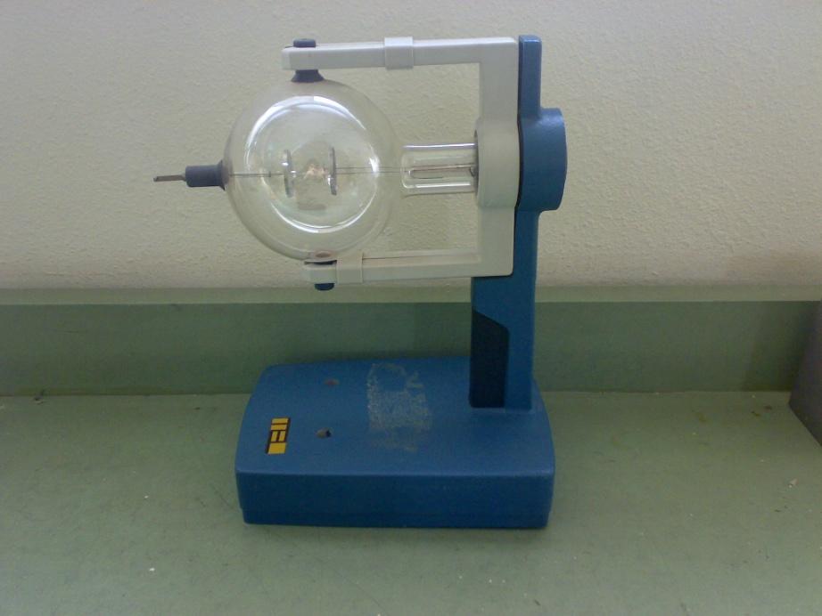
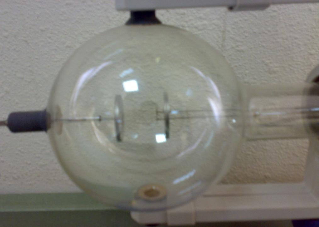
THERMIONIC AND GASEOUS STATE DIODES
 THERMIONIC AND GASEOUS STATE DIODES Thermionic and gaseous state (vacuum tube) diodes Thermionic diodes are thermionic-valve devices (also known as vacuum tubes, tubes, or valves), which are arrangements
Physics 160 Lecture 5. R. Johnson April 13, 2015
 Physics 160 Lecture 5 R. Johnson April 13, 2015 Half Wave Diode Rectifiers Full Wave April 13, 2015 Physics 160 2 Note that there is no ground connection on this side of the rectifier! Output Smoothing
Electronics The basics of semiconductor physics
 Electronics The basics of semiconductor physics Prof. Márta Rencz, Gábor Takács BME DED 17/09/2015 1 / 37 The basic properties of semiconductors Range of conductivity [Source: http://www.britannica.com]
Chapter 1 Introduction to Electronics
 Chapter 1 Introduction to Electronics Section 1-1 Atomic Structure 1. An atom with an atomic number of 6 has 6 electrons and 6 protons.. The third shell of an atom can have n = (3) = 18 electrons. Section
MAHARASHTRA STATE BOARD OF TECHNICAL EDUCATION (Autonomous) (ISO/IEC Certified) Subject Code: Model Answer Page No: 1/
 (ISO/IEC Certified) Subject Code: Model Answer Page No: 1/") MAHARASHTRA STATE BOARD OF TECHNICAL EDUCATION (Autonomous) (ISO/IEC 27001 2005 Certified) SUMMER 13 EXAMINATION Subject Code: 12025 Model Answer Page No: 1/ Important Instructions to examiners: 1) The
MAHARASHTRA STATE BOARD OF TECHNICAL EDUCATION (Autonomous) (ISO/IEC 27001 2005 Certified) SUMMER 13 EXAMINATION Subject Code: 12025 Model Answer Page No: 1/ Important Instructions to examiners: 1) The
Lecture 7:PN Junction. Structure, Depletion region, Different bias Conditions, IV characteristics, Examples
 Lecture 7:PN Junction Structure, Depletion region, Different bias Conditions, IV characteristics, Examples PN Junction The diode (pn junction) is formed by dopping a piece of intrinsic silicon, such that
جامعة اإلسكندرية كلية الهندسة قسم الهندسة الكهربية أبريل ٢٠١٥
 Alexandria University Faculty of Engineering Electrical Engineering Department April 2015 1a EE 132 Electronic Devices and Circuits First Year Time allowed: 1½ hours جامعة اإلسكندرية كلية الهندسة قسم الهندسة
SUMMER 13 EXAMINATION Subject Code: Model Answer Page No: / N
 Important Instructions to examiners: 1) The answers should be examined by key words and not as word-to-word as given in the model answer scheme. 2) The model answer and the answer written by candidate
KOM2751 Analog Electronics :: Dr. Muharrem Mercimek :: YTU - Control and Automation Dept. 1 1 (CONT D) DIODES
 DIODES") KOM2751 Analog Electronics :: Dr. Muharrem Mercimek :: YTU - Control and Automation Dept. 1 1 (CONT D) DIODES Most of the content is from the textbook: Electronic devices and circuit theory, Robert L.
KOM2751 Analog Electronics :: Dr. Muharrem Mercimek :: YTU - Control and Automation Dept. 1 1 (CONT D) DIODES Most of the content is from the textbook: Electronic devices and circuit theory, Robert L.
Lecture 2 p-n junction Diode characteristics. By Asst. Prof Dr. Jassim K. Hmood
 Electronic I Lecture 2 p-n junction Diode characteristics By Asst. Prof Dr. Jassim K. Hmood THE p-n JUNCTION DIODE The pn junction diode is formed by fabrication of a p-type semiconductor region in intimate
Diode conducts when V anode > V cathode. Positive current flow. Diodes (and transistors) are non-linear device: V IR!
 are non-linear device: V IR!") Diodes: What do we use diodes for? Lecture 5: Diodes and Transistors protect circuits by limiting the voltage (clipping and clamping) turn AC into DC (voltage rectifier) voltage multipliers (e.g. double
Diodes: What do we use diodes for? Lecture 5: Diodes and Transistors protect circuits by limiting the voltage (clipping and clamping) turn AC into DC (voltage rectifier) voltage multipliers (e.g. double
Student Lecture by: Giangiacomo Groppi Joel Cassell Pierre Berthelot September 28 th 2004
 Student Lecture by: Giangiacomo Groppi Joel Cassell Pierre Berthelot September 28 th 2004 Lecture outline Historical introduction Semiconductor devices overview Bipolar Junction Transistor (BJT) Field
EC6202- ELECTRONIC DEVICES AND CIRCUITS UNIT TEST-1 EXPECTED QUESTIONS
 EC6202- ELECTRONIC DEVICES AND CIRCUITS UNIT TEST-1 EXPECTED QUESTIONS 1. List the PN diode parameters. 1. Bulk Resistance. 2. Static Resistance/Junction Resistance (or) DC Forward Resistance 3. Dynamic
Syllabus. F.Y.B.Sc. (IT) Electronics and Communication Technology
 Electronics and Communication Technology") Syllabus F.Y.B.Sc. (IT) Electronics and Communication Technology Unit I : Concept of Conductor, Senmiconductor, Insulator, Semiconductor Diode, Forward bias, Reverse Bias, Application of Diode as Rectifier,
Syllabus F.Y.B.Sc. (IT) Electronics and Communication Technology Unit I : Concept of Conductor, Senmiconductor, Insulator, Semiconductor Diode, Forward bias, Reverse Bias, Application of Diode as Rectifier,
Digital Integrated Circuits A Design Perspective. The Devices. Digital Integrated Circuits 2nd Devices
 Digital Integrated Circuits A Design Perspective The Devices The Diode The diodes are rarely explicitly used in modern integrated circuits However, a MOS transistor contains at least two reverse biased
EECE251 Circuit Analysis I Set 6: Diodes
 EECE251 Circuit Analysis I Set 6: Diodes Shahriar Mirabbasi Department of Electrical and Computer Engineering University of British Columbia shahriar@ece.ubc.ca Thanks to Dr. Linares and Dr. Yan for sharing
Semiconductor Materials and Diodes
 C C H H A A P P T T E E R R 1 Semiconductor Materials and Diodes 1.0 1.0 PREVIEW PREVIEW This text deals with the analysis and design of circuits containing electronic devices, such as diodes and transistors.
UNIT-I SEMICONDUCTOR DEVICES
 SEMICONDUCTOR MATERIALS: UNIT-I SEMICONDUCTOR DEVICES INSULATOR: An insulator is a material that offers a very low level of conductivity under Pressure from an applied voltage source. In this material
Class XII - Physics Semiconductor Electronics. Chapter-wise Problems
 lass X - Physics Semiconductor Electronics Materials, Device and Simple ircuit hapter-wise Problems Multiple hoice Question :- 14.1 The conductivity of a semiconductor increases with increase in temperature
2 MARKS EE2203 ELECTRONIC DEVICES AND CIRCUITS UNIT 1
 2 MARKS EE2203 ELECTRONIC DEVICES AND CIRCUITS UNIT 1 1. Define PN junction. When a p type semiconductor is joined to a N type semiconductor the contact surface is called PN junction. 2. What is an ideal
This tutorial will suit all beginners who want to learn the fundamental concepts of transistors and transistor amplifier circuits.
 About the Tutorial An electronic signal contains some information which cannot be utilized if doesn t have proper strength. The process of increasing the signal strength is called as Amplification. Almost
Lecture 3: Diodes. Amplitude Modulation. Diode Detection.
 Whites, EE 322 Lecture 3 Page 1 of 10 Lecture 3: Diodes. Amplitude Modulation. Diode Detection. Diodes are the fourth basic discrete component listed in Lecture 2. These and transistors are both nonlinear
EC T34 ELECTRONIC DEVICES AND CIRCUITS
 RAJIV GANDHI COLLEGE OF ENGINEERING AND TECHNOLOGY PONDY-CUDDALORE MAIN ROAD, KIRUMAMPAKKAM-PUDUCHERRY DEPARTMENT OF ECE EC T34 ELECTRONIC DEVICES AND CIRCUITS II YEAR Mr.L.ARUNJEEVA., AP/ECE 1 PN JUNCTION
Laboratory No. 01: Small & Large Signal Diode Circuits. Electrical Enginnering Departement. By: Dr. Awad Al-Zaben. Instructor: Eng.
 Laboratory No. 01: Small & Large Signal Diode Circuits Electrical Enginnering Departement By: Dr. Awad Al-Zaben Instructor: Eng. Tamer Shahta Electronics Laboratory EE 3191 February 23, 2014 I. OBJECTIVES
Chapter 2. Diodes & Applications
 Chapter 2 Diodes & Applications The Diode A diode is made from a small piece of semiconductor material, usually silicon, in which half is doped as a p region and half is doped as an n region with a pn
Section:A Very short answer question
 Section:A Very short answer question 1.What is the order of energy gap in a conductor, semi conductor, and insulator?. Conductor - no energy gap Semi Conductor - It is of the order of 1 ev. Insulator -
Basic Electronics Important questions
 Basic Electronics Important questions B.E-2/4 Mech- B Faculty: P.Lakshmi Prasanna Note: Read the questions in the following order i. Assignment questions ii. Class test iii. Expected questions iv. Tutorials
3A.1. Lecture 3A Semiconductors. Semiconductor Structure
 3A.1 Lecture 3A Semiconductors Semiconductor structure. ptype semiconductor. ntype semiconductor. The pn junction. The pn junction characteristic (diode vi characteristic). Diode models. The Halleffect
Basic Electronics: Diodes and Transistors. October 14, 2005 ME 435
 Basic Electronics: Diodes and Transistors Eşref Eşkinat E October 14, 2005 ME 435 Electric lectricity ity to Electronic lectronics Electric circuits are connections of conductive wires and other devices
Mathematics and Science in Schools in Sub-Saharan Africa
 Mathematics and Science in Schools in Sub-Saharan Africa SEMICONDUCTORS What is a Semiconductor? What is a Semiconductor? Microprocessors LED Transistors Capacitors Range of Conduciveness The semiconductors
Lesson Plan. Week Theory Practical Lecture Day. Topic (including assignment / test) Day. Thevenin s theorem, Norton s theorem
 Day. Thevenin s theorem, Norton s theorem") Name of the faculty: GYANENDRA KUMAR YADAV Discipline: APPLIED SCIENCE(C.S.E,E.E.ECE) Year : 1st Subject: FEEE Lesson Plan Lesson Plan Duration: 31 weeks (from July, 2018 to April, 2019) Week Theory Practical
Name of the faculty: GYANENDRA KUMAR YADAV Discipline: APPLIED SCIENCE(C.S.E,E.E.ECE) Year : 1st Subject: FEEE Lesson Plan Lesson Plan Duration: 31 weeks (from July, 2018 to April, 2019) Week Theory Practical
ELECTRONIC DEVICES AND CIRCUITS
 ELECTRONIC DEVICES AND CIRCUITS 1. At room temperature the current in an intrinsic semiconductor is due to A. holes B. electrons C. ions D. holes and electrons 2. Work function is the maximum energy required
SEMICONDUCTOR ELECTRONICS: MATERIALS, DEVICES AND SIMPLE CIRCUITS. Class XII : PHYSICS WORKSHEET
 SEMICONDUCT ELECTRONICS: MATERIALS, DEVICES AND SIMPLE CIRCUITS Class XII : PHYSICS WKSHEET 1. How is a n-p-n transistor represented symbolically? (1) 2. How does conductivity of a semiconductor change
Microelectronic Circuits Fourth Edition Adel S. Sedra, Kenneth C. Smith, 1998 Oxford University Press
 Diodes ELZ 206 - Elektronik I Microelectronic Circuits Fourth Edition Adel S. Sedra, Kenneth C. Smith, 1998 Oxford University Press Department of Electrical and Electronics Engineering Dicle University
Semiconductor Diodes
 Semiconductor Diodes A) Motivation and Game Plan B) Semiconductor Doping and Conduction C) Diode Structure and I vs. V D) Diode Circuits Reading: Schwarz and Oldham, Chapter 13.1-13.2 Motivation Digital
Semiconductor Materials and P-I Junctions
 outline 22-1 Semiconductor materials 22-2 The P-N junction OBJECTIVES Ater studying this chapter, you should be able to: 1. Describe the difference between valence electrons and conduction-band electrons
SEMICONDUCTORS Part 1
 Reading 24 Ron Bertrand VK2DQ http://www.radioelectronicschool.com SEMICONDUCTORS Part 1 The objective of this reading and the following, is to provide a basic coverage of the most generally employed solid
LED lecture. Wei Chih Wang University of Washington
 LED lecture Wei Chih Wang University of Washington Linear and Nonlinear electronics current voltage Vaccum tube (i.e. type 2A3) voltage Thermistor (large negative temperature coefficient of resistivity)
Semiconductor Devices Lecture 5, pn-junction Diode
 Semiconductor Devices Lecture 5, pn-junction Diode Content Contact potential Space charge region, Electric Field, depletion depth Current-Voltage characteristic Depletion layer capacitance Diffusion capacitance
CHAPTER SEMI-CONDUCTING DEVICES QUESTION & PROBLEM SOLUTIONS
 Solutions--Ch. 15 (Semi-conducting Devices) CHAPTER 15 -- SEMI-CONDUCTING DEVICES QUESTION & PROBLEM SOLUTIONS 15.1) What is the difference between a conductor and a semi-conductor? Solution: A conductor
SETH JAI PARKASH POLYTECHNIC, DAMLA
 SETH JAI PARKASH POLYTECHNIC, DAMLA NAME OF FACULTY----------SANDEEP SHARMA DISCIPLINE---------------------- E.C.E (S.F) SEMESTER-------------------------2 ND SUBJECT----------------------------BASIC ELECTRONICS
SYED AMMAL ENGINEERING COLLEGE
 SYED AMMAL ENGINEERING COLLEGE (Approved by the AICTE, New Delhi, Govt. of Tamilnadu and Affiliated to Anna University, Chennai) Established in 1998 - An ISO 9001:2008 Certified Institution Dr. E.M.Abdullah
Mechatronics Chapter 3-1 Semiconductor devices Diode
 MEMS1082 Mechatronics Chapter 3-1 Semiconductor devices Diode Semiconductor: Si Semiconductor N-type and P-type Semiconductors There are two types of impurities: N-type - In N-type doping, phosphorus or
Part I Lectures 1-7 Diode Circuit Applications
 Part Lectures -7 iode Circuit Applications The PN Junction iode Electrical and Electronic Engineering epartment Lecture One - Page of 7 Second Year, Electronics, 9 - The PN Junction iode Basic Construction:
Theory. Week. Lecture Day. TOPICS Week TOPICS. Intoduction Overview of DC Circuits. 1.use of measuring instruments-multimeter,cro etc.
 Name of faculty: Sanjay Puri Discipline: Applied Science (Electronics and Communication Engg.) Subject: Fundamentals of Electrical and Electronics Engg. Lesson Plan Duration: 36 weeks (From August 2018
Chapter 1: Diode circuits
 Analog Electronics Circuits Nagamani A N Lecturer, PESIT, Bangalore 85 Email nagamani@pes.edu Chapter 1: Diode circuits Objective To understand the diode operation and its equivalent circuits To understand
Lecture # 23 Diodes and Diode Circuits. A) Basic Semiconductor Materials B) Diode Current and Equation C) Diode Circuits
 Basic Semiconductor Materials B) Diode Current and Equation C) Diode Circuits") EECS 42 ntro. Digital Electronics, Fall 2003 EECS 42 ntroduction to Digital Electronics Lecture # 23 Diodes and Diode Circuits A) Basic Semiconductor Materials B) Diode Current and Equation C) Diode Circuits
EECS 42 ntro. Digital Electronics, Fall 2003 EECS 42 ntroduction to Digital Electronics Lecture # 23 Diodes and Diode Circuits A) Basic Semiconductor Materials B) Diode Current and Equation C) Diode Circuits
Downloaded from
 9. ELECTRONIC DEVICES GIST In metals, the conduction band and valence band partly overlap each other and there is no forbidden energy gap. In insulators, the conduction band is empty and valence band is
PROLOGUE TO ELECTRONICS
 PROLOGUE TO ELECTRONICS When most of us hear the word electronics, we think of televisions, laptop computers, cell phones, or ipods. Actually, these items are electronic systems composed of subsystems
Material Provided by JNTU World
 ELECTRON It is a stable elementary particle with a charge of negative electricity, found in all atoms and acting as the primary carrier of electricity in solids. ELECTRONICS Electronics is the movement
ANALOG ELECTRONICS (AE)
") ANALOG ELECTRONICS (AE) ABOUT COURSE& MARKS SCHEME: 1 Prepared by: BE-EC Amish J. Tankariya SEMESTER-III SUBJECT- ANALOG ELECTRONICS (AE) GTU Subject Code :- 2130902 2 SYLLABUS: 3 4 1 REFERENCE BOOKS:
ANALOG ELECTRONICS (AE) ABOUT COURSE& MARKS SCHEME: 1 Prepared by: BE-EC Amish J. Tankariya SEMESTER-III SUBJECT- ANALOG ELECTRONICS (AE) GTU Subject Code :- 2130902 2 SYLLABUS: 3 4 1 REFERENCE BOOKS:
Diodes. Analog Electronics Lesson 4. Objectives and Overview:
 Analog Electronics Lesson 4 Diodes Objectives and Overview: This lesson will introduce p- and n-type material, how they form a junction that rectifies current, and familiarize you with basic p-n junction