10/27/2009 Reading: Chapter 10 of Hambley Basic Device Physics Handout (optional)
|
|
|
- Cornelius Williams
- 5 years ago
- Views:
Transcription
1 EE40 Lec 17 PN Junctions Prof. Nathan Cheung 10/27/2009 Reading: Chapter 10 of Hambley Basic Device Physics Handout (optional) Slide 1
2 PN Junctions Semiconductor Physics of pn junctions (for reference only) Diode Current and Equation Solar Cells, Photo Detectors, Zener Diodes Load Line Analysis Slide 2
3 The Periodic Table III IV V Slide 3
4 4 nearest neighbors unit cell length = 5.43Å 1s, 2s, 2p orbitals filled by 10 electrons 3s, 3p orbitals filled by 4 electrons The Si Atom atoms/cm 3 The Si Crystal diamond cubic structure Slide 4

 = p (hole conc) = n i")
5 Pure Si is not very conductive electron - Bottom of conduction band Energy gap =1.12 ev hole Top of valence band n (electron conc) = p (hole conc) = n i Slide 5 5
6 Shockley s Parking Garage Analogy for Conduction in Si Two-story parking garage on a hill: If the lower floor is full and top one is empty, no traffic is possible. Analog of an insulator. All electrons are locked up. Slide 6
7 Doping By substituting a Si atom with a special impurity atom (Column V or Column III element), a conduction electron or hole is created. Donors: P, As, Sb Acceptors: B, Al, Ga, In Dopant concentrations typically range from cm -3 to cm -3 Slide 7
8 Semiconductor with both acceptors and donors has 4 kinds of charge carriers Hole Electron Mobile Charge Carriers they contribute to current flow with electric field is applied. Ionized Immobile Charges Donor they DO NOT contribute to current flow Ionized with electric field is applied. Acceptor However, they affect the local lelectric field Slide 8 8
9 Charge Neutrality Condition Even N A is not equal to N D, microscopic volume surrounding any position x has zero net charge Valid for homogeneously doped semiconductor at thermal equilibrium Si atom (neutral) Ionized Donor Ionized Acceptor Hole Electron Electrons and holes created by Si atoms with conc n i Slide 9 9
10 Shockley s Parking Garage Analogy for Conduction in Si Two-story parking garage on a hill: If one car is moved upstairs, it can move AND THE HOLE ON THE LOWER FLOOR CAN MOVE. Conduction is possible. Analog to warmed-up semiconductor. Some electrons get free (and leave holes behind). Slide 10
11 Shockley s Parking Garage Analogy for Conduction in Si Two-story parking garage on a hill: If an extra car is donated to the upper floor, it can move. Conduction is possible. Analog to N-type semiconductor. (An electron donor is added to the crystal, creating free electrons). Slide 11
12 Shockley s Parking Garage Analogy for Conduction in Si Two-story parking garage on a hill: If a car is removed from the lower floor, it leaves a HOLE which can move. Conduction is possible. Analog to P-type semiconductor. (Acceptors are added to the crystal, consuming bonding electrons,creating free holes). Slide 12
13 Summary of n- and p-type silicon Pure silicon is an insulator. At high temperatures it conducts weakly. If we add an impurity with extra electrons (e.g. arsenic, phosphorus) p these extra electrons are set free and we have a pretty good conductor (n-type silicon). If we add an impurity with a deficit of electrons (e.g. boron) then bonding electrons are missing (holes), and the resulting holes can move around again a pretty good conductor (p-type silicon) Now what is really interesting is when we join n-type and p-type silicon, that is make a pn junction. It has interesting electrical properties. Slide 13
14 Junctions of n- and p-type Regions What happens to the electrons and holes when n and p regions are brought into contact : aluminum? aluminum wire n p Slide 14
15 The pn Junction Diode Schematic diagram p-type n-type Circuit symbol I D net acceptor concentration N A net donor concentration N D cross-sectional area A D V D Physical structure: I (an example) D metal SiO 2 SiO 2 For simplicity, assume that the doping profile changes abruptly at the junction. V D p-type Si n-type Si metal Slide 15
16 Depletion Region Approximation When the junction is first formed, mobile carriers diffuse across the junction (due to the concentration gradients) Holes diffuse from the psideto the n side, leaving behind negatively charged immobile acceptor ions Electrons diffuse from the n side to the p side, leaving behind positively charged immobile donor ions acceptor ions donor ions p A region depleted of mobile carriers is formed at the junction. The space charge due to immobile ions in the depletion region establishes an electric field that opposes carrier diffusion. n Slide 16
17 Charge Density Distribution and Electric Field Unbalanced Charge is created in the depletion region. acceptor ions donor ions p n quasi-neutral p region depletion region quasi-neutral n region charge density (C/cm 3 ) distance - Build-in electric field Slide 17
18 Effect of Applied Voltage V p D n The quasi-neutral p and n regions have low resistivity, whereas the depletion region has high resistivity. Thus, when an external voltage V D is applied across the diode, almost all of this voltage is dropped across the depletion region. (Think of a voltage divider circuit.) If V D > 0 (forward bias), depletion charge reduced If V D < 0 (reverse bias), depletion charge increased Slide 18
19 Slide 19
20 Slide 20 20
21 Diode Physical Behavior and Equation Schematic Device N P type type V I Symbol V I Qualitative I-V characteristics: I V positive, easy conduction Quantitative I-V characteristics: I qv kt = I0 0( (e 1) V negative, no conduction In which kt/q is 0.026V and I O is a V constant t depending di on diode d area. Typical values: to A.. A non-ideality factor n times kt/q is often included. Slide 21
22 The pn Junction I vs. V Equation I-V characteristic of PN junctions In EECS 105, 130, and other courses you will learn why the I vs. V relationship for PN junctions is of the form I qv kt = I0( (e 1) where I 0 is a constant proportional to junction area and depending on doping in P and N regions, 19 q = electronic charge = , k is Boltzman constant, and T is absolute temperature. KT q = 0.026V at300 K, a typical value for I 0 is A We note that in forward bias, I increases exponentially and is in the µa-ma range for voltages typically in the range of V. In reverse bias, the current is essentially zero. Slide 22
23 I D Ideal Diode Model of PN Diode Circuit symbol I-V characteristic Switch model I D (A) V D forward bias reverse bias V D (V) I D V D An ideal diode passes current only in one direction. An ideal diode has the following properties: when I D > 0, V D = 0 when V D < 0, I D = 0 Diode behaves like a switch: closed in forward bias mode open in reverse bias mode Slide 23
24 Piecewise Linear Model Circuit symbol I-V characteristic Switch model I D I D (A) I D V Don V D forward bias reverse bias V D (V) V Don V D For a Si pn diode, V Don 0.7 V RULE 1: When I D > 0, V D = V Don RULE 2: When V D < V Don, I D = 0 Diode behaves like a voltage source in series with a switch: closed in forward bias mode open in reverse erse bias mode Slide 24
25 pn-junction Reverse Breakdown As the reverse bias voltage increases, the peak electric field in the depletion region increases. When the electric field exceeds a critical value (E crit 2x10 5 V/cm), the reverse current shows a dramatic increase: reverse (leakage) current I D (A) forward current breakdown voltage V BD V D (V) - 10 to -100V Slide 25
26 Load Line Analysis Method 1. Graph the I-V relationships for the non-linear element and for the rest of the circuit 2. The operating point of the circuit it is found from the intersection of these two curves. R Th I I V Th V V Th /R Th operating point V V Th The I-V characteristic of all of the circuit except the non-linear element is called the load line Slide 26


27 Solar cell: Example of simple PN junction What is a solar cell? Device that converts sunlight into electricity it How does it work? In simple configuration, it is a diode made of PN junction Incident light is absorbed b by material Creates electron-hole pairs that transport through the material through Diffusion (concentration gradient) Drift (due to electric field) PN Junction Diode Slide 27
28 Slide 28
29 How PVs work Semiconductor can absorb light (photons) and convert them to current (carriers) We modify the semiconductor (create a pn junction) to harvest the carriers Slide 29
30 Photovoltaic (Solar) Cell I D qvd kt = I S ( e 1) I optical I D (A) in the dark V D (V) with incident light Operating point The load line a simple resistor. Slide 30
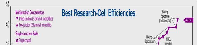
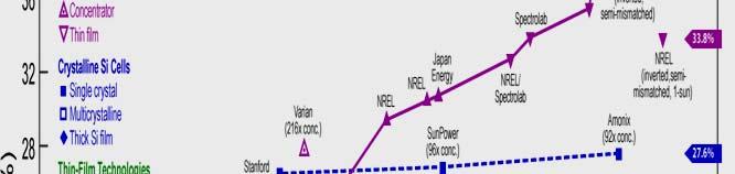
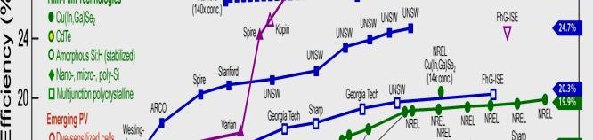
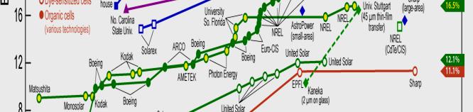
31 Cell Efficiencies Slide 31
32 Photo Diode R Th I I V Th V operating points under different light conditions. As light intensity increases. Why? V Th V As light shines on the photodiode, carriers are generated by absorption. These excess carriers are swept by the electric field at the junction creating drift current, which is same direction as the reverse bias current and hence negative current. The current is proportional to light intensity and hence can provide a direct measurement of light intensity photodetector. V Th /R Th load line Slide 32
33 Zener Diode A Zener diode is designed to operate in the breakdown mode With a well defined breakdown voltage. (l k ) t I D (A) reverse (leakage) current forward current breakdown voltage V BD V D (V) Example: v s (t) R V BD = 15V v o (t) t integrated circuit Slide 33
Semiconductor Diodes
 Semiconductor Diodes A) Motivation and Game Plan B) Semiconductor Doping and Conduction C) Diode Structure and I vs. V D) Diode Circuits Reading: Schwarz and Oldham, Chapter 13.1-13.2 Motivation Digital
Lecture # 23 Diodes and Diode Circuits. A) Basic Semiconductor Materials B) Diode Current and Equation C) Diode Circuits
 Basic Semiconductor Materials B) Diode Current and Equation C) Diode Circuits") EECS 42 ntro. Digital Electronics, Fall 2003 EECS 42 ntroduction to Digital Electronics Lecture # 23 Diodes and Diode Circuits A) Basic Semiconductor Materials B) Diode Current and Equation C) Diode Circuits
EECS 42 ntro. Digital Electronics, Fall 2003 EECS 42 ntroduction to Digital Electronics Lecture # 23 Diodes and Diode Circuits A) Basic Semiconductor Materials B) Diode Current and Equation C) Diode Circuits
Intrinsic Semiconductor
 Semiconductors Crystalline solid materials whose resistivities are values between those of conductors and insulators. Good electrical characteristics and feasible fabrication technology are some reasons
Electronic devices-i. Difference between conductors, insulators and semiconductors
 Electronic devices-i Semiconductor Devices is one of the important and easy units in class XII CBSE Physics syllabus. It is easy to understand and learn. Generally the questions asked are simple. The unit
Electronics The basics of semiconductor physics
 Electronics The basics of semiconductor physics Prof. Márta Rencz, Gábor Takács BME DED 17/09/2015 1 / 37 The basic properties of semiconductors Range of conductivity [Source: http://www.britannica.com]
Semiconductor Devices Lecture 5, pn-junction Diode
 Semiconductor Devices Lecture 5, pn-junction Diode Content Contact potential Space charge region, Electric Field, depletion depth Current-Voltage characteristic Depletion layer capacitance Diffusion capacitance
Electronic Circuits I. Instructor: Dr. Alaa Mahmoud
 Electronic Circuits I Instructor: Dr. Alaa Mahmoud alaa_y_emam@hotmail.com Chapter 27 Diode and diode application Outline: Semiconductor Materials The P-N Junction Diode Biasing P-N Junction Volt-Ampere
Ch5 Diodes and Diodes Circuits
 Circuits and Analog Electronics Ch5 Diodes and Diodes Circuits 5.1 The Physical Principles of Semiconductor 5.2 Diodes 5.3 Diode Circuits 5.4 Zener Diode References: Floyd-Ch2; Gao-Ch6; 5.1 The Physical
Università degli Studi di Roma Tor Vergata Dipartimento di Ingegneria Elettronica. Analogue Electronics. Paolo Colantonio A.A.
 Università degli Studi di Roma Tor Vergata Dipartimento di Ingegneria Elettronica Analogue Electronics Paolo Colantonio A.A. 2015-16 Introduction: materials Conductors e.g. copper or aluminum have a cloud
PN Junction Diode Table of Contents. What Are Diodes Made Out Of?
 PN Junction iode Table of Contents What are diodes made out of?slide 3 N-type materialslide 4 P-type materialslide 5 The pn junctionslides 6-7 The biased pn junctionslides 8-9 Properties of diodesslides
Digital Integrated Circuits A Design Perspective. The Devices. Digital Integrated Circuits 2nd Devices
 Digital Integrated Circuits A Design Perspective The Devices The Diode The diodes are rarely explicitly used in modern integrated circuits However, a MOS transistor contains at least two reverse biased
KOM2751 Analog Electronics :: Dr. Muharrem Mercimek :: YTU - Control and Automation Dept. 1 1 (CONT D) DIODES
 DIODES") KOM2751 Analog Electronics :: Dr. Muharrem Mercimek :: YTU - Control and Automation Dept. 1 1 (CONT D) DIODES Most of the content is from the textbook: Electronic devices and circuit theory, Robert L.
KOM2751 Analog Electronics :: Dr. Muharrem Mercimek :: YTU - Control and Automation Dept. 1 1 (CONT D) DIODES Most of the content is from the textbook: Electronic devices and circuit theory, Robert L.
Department of Electrical Engineering IIT Madras
 Department of Electrical Engineering IIT Madras Sample Questions on Semiconductor Devices EE3 applicants who are interested to pursue their research in microelectronics devices area (fabrication and/or
NAME: Last First Signature
 UNIVERSITY OF CALIFORNIA, BERKELEY College of Engineering Department of Electrical Engineering and Computer Sciences EE 130: IC Devices Spring 2003 FINAL EXAMINATION NAME: Last First Signature STUDENT
Sharjah Indian School, Sharjah ELECTRONIC DEVICES - Class XII (Boys Wing) Page 01
 Page 01") ELECTRONIC DEVICES - Class XII (Boys Wing) Page 01 Electronics is the fast developing branch of Physics. Before the discovery of transistors in 1948, vacuum tubes (thermionic valves) were used as the building
ELECTRONIC DEVICES - Class XII (Boys Wing) Page 01 Electronics is the fast developing branch of Physics. Before the discovery of transistors in 1948, vacuum tubes (thermionic valves) were used as the building
CHAPTER 8 The PN Junction Diode
 CHAPTER 8 The PN Junction Diode Consider the process by which the potential barrier of a PN junction is lowered when a forward bias voltage is applied, so holes and electrons can flow across the junction
EC T34 ELECTRONIC DEVICES AND CIRCUITS
 RAJIV GANDHI COLLEGE OF ENGINEERING AND TECHNOLOGY PONDY-CUDDALORE MAIN ROAD, KIRUMAMPAKKAM-PUDUCHERRY DEPARTMENT OF ECE EC T34 ELECTRONIC DEVICES AND CIRCUITS II YEAR Mr.L.ARUNJEEVA., AP/ECE 1 PN JUNCTION
Photodiode: LECTURE-5
 LECTURE-5 Photodiode: Photodiode consists of an intrinsic semiconductor sandwiched between two heavily doped p-type and n-type semiconductors as shown in Fig. 3.2.2. Sufficient reverse voltage is applied
Laboratory No. 01: Small & Large Signal Diode Circuits. Electrical Enginnering Departement. By: Dr. Awad Al-Zaben. Instructor: Eng.
 Laboratory No. 01: Small & Large Signal Diode Circuits Electrical Enginnering Departement By: Dr. Awad Al-Zaben Instructor: Eng. Tamer Shahta Electronics Laboratory EE 3191 February 23, 2014 I. OBJECTIVES
THERMIONIC AND GASEOUS STATE DIODES
 THERMIONIC AND GASEOUS STATE DIODES Thermionic and gaseous state (vacuum tube) diodes Thermionic diodes are thermionic-valve devices (also known as vacuum tubes, tubes, or valves), which are arrangements
Lesson 08. Name and affiliation of the author: Professor L B D R P Wijesundera Department of Physics, University of Kelaniya.
 Lesson 08 Title of the Experiment: Identification of active components in electronic circuits and characteristics of a Diode, Zener diode and LED (Activity number of the GCE Advanced Level practical Guide
 Electronic Devices 1. Current flowing in each of the following circuits A and respectively are: (Circuit 1) (Circuit 2) 1) 1A, 2A 2) 2A, 1A 3) 4A, 2A 4) 2A, 4A 2. Among the following one statement is not
Chapter Semiconductor Electronics
 Chapter Semiconductor Electronics Q1. p-n junction is said to be forward biased, when [1988] (a) the positive pole of the battery is joined to the p- semiconductor and negative pole to the n- semiconductor
UNIT IX ELECTRONIC DEVICES
 UNT X ELECTRONC DECES Weightage Marks : 07 Semiconductors Semiconductors diode-- characteristics in forward and reverse bias, diode as rectifier. - characteristics of LED, Photodiodes, solarcell and Zener
Diode conducts when V anode > V cathode. Positive current flow. Diodes (and transistors) are non-linear device: V IR!
 are non-linear device: V IR!") Diodes: What do we use diodes for? Lecture 5: Diodes and Transistors protect circuits by limiting the voltage (clipping and clamping) turn AC into DC (voltage rectifier) voltage multipliers (e.g. double
Diodes: What do we use diodes for? Lecture 5: Diodes and Transistors protect circuits by limiting the voltage (clipping and clamping) turn AC into DC (voltage rectifier) voltage multipliers (e.g. double
semiconductor p-n junction Potential difference across the depletion region is called the built-in potential barrier, or built-in voltage:
 Chapter four The Equilibrium pn Junction The Electric field will create a force that will stop the diffusion of carriers reaches thermal equilibrium condition Potential difference across the depletion
Lesson 5. Electronics: Semiconductors Doping p-n Junction Diode Half Wave and Full Wave Rectification Introduction to Transistors-
 Lesson 5 Electronics: Semiconductors Doping p-n Junction Diode Half Wave and Full Wave Rectification Introduction to Transistors- Types and Connections Semiconductors Semiconductors If there are many free
CHAPTER 8 The PN Junction Diode
 CHAPTER 8 The PN Junction Diode Consider the process by which the potential barrier of a PN junction is lowered when a forward bias voltage is applied, so holes and electrons can flow across the junction
1 Semiconductor-Photon Interaction
 1 SEMICONDUCTOR-PHOTON INTERACTION 1 1 Semiconductor-Photon Interaction Absorption: photo-detectors, solar cells, radiation sensors. Radiative transitions: light emitting diodes, displays. Stimulated emission:
PHYS 3050 Electronics I
 PHYS 3050 Electronics I Chapter 4. Semiconductor Diodes and Transistors Earth, Moon, Mars, and Beyond Dr. Jinjun Shan, Associate Professor of Space Engineering Department of Earth and Space Science and
Lecture 2 p-n junction Diode characteristics. By Asst. Prof Dr. Jassim K. Hmood
 Electronic I Lecture 2 p-n junction Diode characteristics By Asst. Prof Dr. Jassim K. Hmood THE p-n JUNCTION DIODE The pn junction diode is formed by fabrication of a p-type semiconductor region in intimate
Semiconductor Materials and Diodes
 C C H H A A P P T T E E R R 1 Semiconductor Materials and Diodes 1.0 1.0 PREVIEW PREVIEW This text deals with the analysis and design of circuits containing electronic devices, such as diodes and transistors.
 Energy band diagrams Metals: 9. ELECTRONIC DEVICES GIST ρ= 10-2 to 10-8 Ω m Insulators: ρ> 10 8 Ω m Semiconductors ρ= 1 to 10 5 Ω m 109 A. Intrinsic semiconductors At T=0k it acts as insulator At room
CHAPTER 8 The pn Junction Diode
 CHAPTER 8 The pn Junction Diode Consider the process by which the potential barrier of a pn junction is lowered when a forward bias voltage is applied, so holes and electrons can flow across the junction
EDC Lecture Notes UNIT-1
 P-N Junction Diode EDC Lecture Notes Diode: A pure silicon crystal or germanium crystal is known as an intrinsic semiconductor. There are not enough free electrons and holes in an intrinsic semi-conductor
Analog Electronic Circuits
 Analog Electronic Circuits Chapter 1: Semiconductor Diodes Objectives: To become familiar with the working principles of semiconductor diode To become familiar with the design and analysis of diode circuits
CONTENTS. 2.2 Schrodinger's Wave Equation 31. PART I Semiconductor Material Properties. 2.3 Applications of Schrodinger's Wave Equation 34
 CONTENTS Preface x Prologue Semiconductors and the Integrated Circuit xvii PART I Semiconductor Material Properties CHAPTER 1 The Crystal Structure of Solids 1 1.0 Preview 1 1.1 Semiconductor Materials
Chapter 14 Semiconductor Electronics Materials Devices And Simple Circuits
 Class XII Chapter 14 Semiconductor Electronics Materials Devices And Simple Circuits Physics Question 14.1: In an n-type silicon, which of the following statement is true: (a) Electrons are majority carriers
Key Questions ECE 340 Lecture 28 : Photodiodes
 Things you should know when you leave Key Questions ECE 340 Lecture 28 : Photodiodes Class Outline: How do the I-V characteristics change with illumination? How do solar cells operate? How do photodiodes
LED lecture. Wei Chih Wang University of Washington
 LED lecture Wei Chih Wang University of Washington Linear and Nonlinear electronics current voltage Vaccum tube (i.e. type 2A3) voltage Thermistor (large negative temperature coefficient of resistivity)
Introduction to Photovoltaics
 Introduction to Photovoltaics PHYS 4400, Principles and Varieties of Solar Energy Instructor: Randy J. Ellingson The University of Toledo February 24, 2015 Only solar energy Of all the possible sources
BASIC ELECTRONICS ENGINEERING
 BASIC ELECTRONICS ENGINEERING Objective Questions UNIT 1: DIODES AND CIRCUITS 1 2 3 4 5 6 7 8 9 10 11 12 The process by which impurities are added to a pure semiconductor is A. Diffusing B. Drift C. Doping
EE/COE 152: Basic Electronics. Lecture 3. A.S Agbemenu. https://sites.google.com/site/agbemenu/courses/ee-coe-152
 EE/COE 152: Basic Electronics Lecture 3 A.S Agbemenu https://sites.google.com/site/agbemenu/courses/ee-coe-152 Books: Microelcetronic Circuit Design (Jaeger/Blalock) Microelectronic Circuits (Sedra/Smith)
Physics 160 Lecture 5. R. Johnson April 13, 2015
 Physics 160 Lecture 5 R. Johnson April 13, 2015 Half Wave Diode Rectifiers Full Wave April 13, 2015 Physics 160 2 Note that there is no ground connection on this side of the rectifier! Output Smoothing
EXPERIMENTS USING SEMICONDUCTOR DIODES
 EXPERIMENT 9 EXPERIMENTS USING SEMICONDUCTOR DIODES Semiconductor Diodes Structure 91 Introduction Objectives 92 Basics of Semiconductors Revisited 93 A p-n Junction Operation of a p-n Junction A Forward
EECE251 Circuit Analysis I Set 6: Diodes
 EECE251 Circuit Analysis I Set 6: Diodes Shahriar Mirabbasi Department of Electrical and Computer Engineering University of British Columbia shahriar@ece.ubc.ca Thanks to Dr. Linares and Dr. Yan for sharing
LEDs, Photodetectors and Solar Cells
 LEDs, Photodetectors and Solar Cells Chapter 7 (Parker) ELEC 424 John Peeples Why the Interest in Photons? Answer: Momentum and Radiation High electrical current density destroys minute polysilicon and
What is the highest efficiency Solar Cell?
 What is the highest efficiency Solar Cell? GT CRC Roof-Mounted PV System Largest single PV structure at the time of it s construction for the 1996 Olympic games Produced more than 1 billion watt hrs. of
 SEMICONDUCTOR EECTRONICS MATERIAS, DEVICES AND SIMPE CIRCUITS Important Points: 1. In semiconductors Valence band is almost filled and the conduction band is almost empty. The energy gap is very small
EE70 - Intro. Electronics
 EE70 - Intro. Electronics Course website: ~/classes/ee70/fall05 Today s class agenda (November 28, 2005) review Serial/parallel resonant circuits Diode Field Effect Transistor (FET) f 0 = Qs = Qs = 1 2π
Section 2.3 Bipolar junction transistors - BJTs
 Section 2.3 Bipolar junction transistors - BJTs Single junction devices, such as p-n and Schottkty diodes can be used to obtain rectifying I-V characteristics, and to form electronic switching circuits
PHYSICAL ELECTRONICS(ECE3540) APPLICATIONS OF PHYSICAL ELECTRONICS PART I
 APPLICATIONS OF PHYSICAL ELECTRONICS PART I") PHYSICAL ELECTRONICS(ECE3540) APPLICATIONS OF PHYSICAL ELECTRONICS PART I Tennessee Technological University Monday, October 28, 2013 1 Introduction In the following slides, we will discuss the summary
PHYSICAL ELECTRONICS(ECE3540) APPLICATIONS OF PHYSICAL ELECTRONICS PART I Tennessee Technological University Monday, October 28, 2013 1 Introduction In the following slides, we will discuss the summary
Downloaded from
 SOLID AND SEMICONDUCTOR DEVICES (EASY AND SCORING TOPIC) 1. Distinction of metals, semiconductor and insulator on the basis of Energy band of Solids. 2. Types of Semiconductor. 3. PN Junction formation
IENGINEERS- CONSULTANTS LECTURE NOTES SERIES ELECTRONICS ENGINEERING 1 YEAR UPTU. Lecture-4
 2 P-n Lecture-4 20 Introduction: If a junction is formed between a p-type and a n-type semiconductor this combination is known as p-n junction diode and has the properties of a rectifier 21 Formation of
The Discussion of this exercise covers the following points:
 Exercise 1 The Diode EXERCISE OBJECTIVE When you have completed this exercise, you will be familiar with the operation of a diode. DISCUSSION OUTLINE The Discussion of this exercise covers the following
Discuss the basic structure of atoms Discuss properties of insulators, conductors, and semiconductors
 Discuss the basic structure of atoms Discuss properties of insulators, conductors, and semiconductors Discuss covalent bonding Describe the properties of both p and n type materials Discuss both forward
PROLOGUE TO ELECTRONICS
 PROLOGUE TO ELECTRONICS When most of us hear the word electronics, we think of televisions, laptop computers, cell phones, or ipods. Actually, these items are electronic systems composed of subsystems
EE 5611 Introduction to Microelectronic Technologies Fall Thursday, September 04, 2014 Lecture 02
 EE 5611 Introduction to Microelectronic Technologies Fall 2014 Thursday, September 04, 2014 Lecture 02 1 Lecture Outline Review on semiconductor materials Review on microelectronic devices Example of microelectronic
EFM Ec. a) Sketch the electrostatic potential inside the semiconductor as a function of position.
 Sketch the electrostatic potential inside the semiconductor as a function of position.") 1.The energy band diagram for an ideal x o =.2um MOS-C operated at T=300K is shown below. Note that the applied gate voltage causes band bending in the semiconductor such that E F =E i at the Si-SiO2 interface.
1.The energy band diagram for an ideal x o =.2um MOS-C operated at T=300K is shown below. Note that the applied gate voltage causes band bending in the semiconductor such that E F =E i at the Si-SiO2 interface.
Basic Electronics. Introductory Lecture Course for. Technology and Instrumentation in Particle Physics Chicago, Illinois June 9-14, 2011
 Basic Electronics Introductory Lecture Course for Technology and Instrumentation in Particle Physics 2011 Chicago, Illinois June 9-14, 2011 Presented By Gary Drake Argonne National Laboratory Session 3
Learning Outcomes. Spiral 2-6. Current, Voltage, & Resistors DIODES
 26.1 26.2 Learning Outcomes Spiral 26 Semiconductor Material MOS Theory I underst why a diode conducts current under forward bias but does not under reverse bias I underst the three modes of operation
Review Energy Bands Carrier Density & Mobility Carrier Transport Generation and Recombination
 Review Energy Bands Carrier Density & Mobility Carrier Transport Generation and Recombination Current Transport: Diffusion, Thermionic Emission & Tunneling For Diffusion current, the depletion layer is
Lecture 3: Diodes. Amplitude Modulation. Diode Detection.
 Whites, EE 322 Lecture 3 Page 1 of 10 Lecture 3: Diodes. Amplitude Modulation. Diode Detection. Diodes are the fourth basic discrete component listed in Lecture 2. These and transistors are both nonlinear
Optical Receivers Theory and Operation
 Optical Receivers Theory and Operation Photo Detectors Optical receivers convert optical signal (light) to electrical signal (current/voltage) Hence referred O/E Converter Photodetector is the fundamental
Solar Cell Parameters and Equivalent Circuit
 9 Solar Cell Parameters and Equivalent Circuit 9.1 External solar cell parameters The main parameters that are used to characterise the performance of solar cells are the peak power P max, the short-circuit
SEMICONDUCTOR ELECTRONICS: MATERIALS, DEVICES AND SIMPLE CIRCUITS
 Chapter Fourteen SEMICONDUCTOR ELECTRONICS: MATERIALS, DEVICES AND SIMPLE CIRCUITS 14.1 INTRODUCTION Devices in which a controlled flow of electrons can be obtained are the basic building blocks of all
Wallace Hall Academy. CfE Higher Physics. Unit 3 - Electricity Notes Name
 Wallace Hall Academy CfE Higher Physics Unit 3 - Electricity Notes Name 1 Electrons and Energy Alternating current and direct current Alternating current electrons flow back and forth several times per
PN Junction in equilibrium
 PN Junction in equilibrium PN junctions are important for the following reasons: (i) PN junction is an important semiconductor device in itself and used in a wide variety of applications such as rectifiers,
Downloaded from
 Question 14.1: In an n-type silicon, which of the following statement is true: (a) Electrons are majority carriers and trivalent atoms are the dopants. (b) Electrons are minority carriers and pentavalent
Student Lecture by: Giangiacomo Groppi Joel Cassell Pierre Berthelot September 28 th 2004
 Student Lecture by: Giangiacomo Groppi Joel Cassell Pierre Berthelot September 28 th 2004 Lecture outline Historical introduction Semiconductor devices overview Bipolar Junction Transistor (BJT) Field
Unit 2 Semiconductor Devices. Lecture_2.5 Opto-Electronic Devices
 Unit 2 Semiconductor Devices Lecture_2.5 Opto-Electronic Devices Opto-electronics Opto-electronics is the study and application of electronic devices that interact with light. Electronics (electrons) Optics
Class XII - Physics Semiconductor Electronics. Chapter-wise Problems
 lass X - Physics Semiconductor Electronics Materials, Device and Simple ircuit hapter-wise Problems Multiple hoice Question :- 14.1 The conductivity of a semiconductor increases with increase in temperature
OPTOELECTRONIC and PHOTOVOLTAIC DEVICES
 OPTOELECTRONIC and PHOTOVOLTAIC DEVICES Outline 1. Introduction to the (semiconductor) physics: energy bands, charge carriers, semiconductors, p-n junction, materials, etc. 2. Light emitting diodes Light
Lecture 7:PN Junction. Structure, Depletion region, Different bias Conditions, IV characteristics, Examples
 Lecture 7:PN Junction Structure, Depletion region, Different bias Conditions, IV characteristics, Examples PN Junction The diode (pn junction) is formed by dopping a piece of intrinsic silicon, such that
ECE-342 Test 1: Sep 27, :00-8:00, Closed Book. Name : SOLUTION
 ECE-342 Test 1: Sep 27, 2011 6:00-8:00, Closed Book Name : SOLUTION All solutions must provide units as appropriate. Use the physical constants and data as provided on the formula sheet the last page of
Mechatronics Chapter 3-1 Semiconductor devices Diode
 MEMS1082 Mechatronics Chapter 3-1 Semiconductor devices Diode Semiconductor: Si Semiconductor N-type and P-type Semiconductors There are two types of impurities: N-type - In N-type doping, phosphorus or
Fall 2004 Dawn Hettelsater, Yan Zhang and Ali Shakouri, 05/09/2002
 University of California at Santa Cruz Jack Baskin School of Engineering Electrical Engineering Department EE-145L: Properties of Materials Laboratory Lab 6: Solar Cells Fall 2004 Dawn Hettelsater, Yan
EXPERIMENT 10: SCHOTTKY DIODE CHARACTERISTICS
 EXPERIMENT 10: SCHOTTKY DIODE CHARACTERISTICS AIM: To plot forward and reverse characteristics of Schottky diode (Metal Semiconductor junction) APPARATUS: D.C. Supply (0 15 V), current limiting resistor
1) A silicon diode measures a low value of resistance with the meter leads in both positions. The trouble, if any, is
 A silicon diode measures a low value of resistance with the meter leads in both positions. The trouble, if any, is") 1) A silicon diode measures a low value of resistance with the meter leads in both positions. The trouble, if any, is A [ ]) the diode is open. B [ ]) the diode is shorted to ground. C [v]) the diode is
1) A silicon diode measures a low value of resistance with the meter leads in both positions. The trouble, if any, is A [ ]) the diode is open. B [ ]) the diode is shorted to ground. C [v]) the diode is
Basic Electronics: Diodes and Transistors. October 14, 2005 ME 435
 Basic Electronics: Diodes and Transistors Eşref Eşkinat E October 14, 2005 ME 435 Electric lectricity ity to Electronic lectronics Electric circuits are connections of conductive wires and other devices
10/14/2009. Semiconductor basics pn junction Solar cell operation Design of silicon solar cell
 PHOTOVOLTAICS Fundamentals PV FUNDAMENTALS Semiconductor basics pn junction Solar cell operation Design of silicon solar cell SEMICONDUCTOR BASICS Allowed energy bands Valence and conduction band Fermi
Discuss the difference between conductors,insulators and semi conductors. Understand the P-N junction and explain the origin of the depletion region
 UNIT III SEMICONDUCTOR DIODES Review of intrinsic & externsic semiconductors Theory of PN junction diode Energy band structure current equation space charge and diffusion capacitances effect of temperature
SRM INSTITUTE OF SCIENCE AND TECHNOLOGY (DEEMED UNIVERSITY)
") SRM INSTITUTE OF SCIENCE AND TECHNOLOGY (DEEMED UNIVERSITY) QUESTION BANK I YEAR B.Tech (II Semester) ELECTRONIC DEVICES (COMMON FOR EC102, EE104, IC108, BM106) UNIT-I PART-A 1. What are intrinsic and
SRM INSTITUTE OF SCIENCE AND TECHNOLOGY (DEEMED UNIVERSITY) QUESTION BANK I YEAR B.Tech (II Semester) ELECTRONIC DEVICES (COMMON FOR EC102, EE104, IC108, BM106) UNIT-I PART-A 1. What are intrinsic and
EECE 481. MOS Basics Lecture 2
 EECE 481 MOS Basics Lecture 2 Reza Molavi Dept. of ECE University of British Columbia reza@ece.ubc.ca Slides Courtesy : Dr. Res Saleh (UBC), Dr. D. Sengupta (AMD), Dr. B. Razavi (UCLA) 1 PN Junction and
Lab VIII Photodetectors ECE 476
 Lab VIII Photodetectors ECE 476 I. Purpose The electrical and optical properties of various photodetectors will be investigated. II. Background Photodiode A photodiode is a standard diode packaged so that
Digital Integrated Circuits EECS 312
 14 12 10 8 6 Fujitsu VP2000 IBM 3090S Pulsar 4 IBM 3090 IBM RY6 CDC Cyber 205 IBM 4381 IBM RY4 2 IBM 3081 Apache Fujitsu M380 IBM 370 Merced IBM 360 IBM 3033 Vacuum Pentium II(DSIP) 0 1950 1960 1970 1980
Electronics I. Midterm #1
 The University of Toledo s6ms_elct7.fm - Electronics I Midterm # Problems Points. 4 2. 5 3. 6 Total 5 Was the exam fair? yes no The University of Toledo s6ms_elct7.fm - 2 Problem 4 points For full credit,
Microelectronic Circuits Fourth Edition Adel S. Sedra, Kenneth C. Smith, 1998 Oxford University Press
 Diodes ELZ 206 - Elektronik I Microelectronic Circuits Fourth Edition Adel S. Sedra, Kenneth C. Smith, 1998 Oxford University Press Department of Electrical and Electronics Engineering Dicle University
Figure 2.1: Energy Band gap Block Diagram
 Figure 2.1: Energy Band gap Block Diagram Figure 2.2: Log Is Vs 10 3 /T Figure 2.3: Schematic Representation of a p-n Junction Diode Department of Physical Sciences, Bannari Amman Institute of Technology,
Detectors for Optical Communications
 Optical Communications: Circuits, Systems and Devices Chapter 3: Optical Devices for Optical Communications lecturer: Dr. Ali Fotowat Ahmady Sep 2012 Sharif University of Technology 1 Photo All detectors
15 - SEMICONDUCTOR ELECTRONICS: MATERIALS, DEVICES AND SIMPLE CIRCUITS Page 1
 15.1 Introduction MATERIALS, DEVICES AND SIMPLE CIRCUITS Page 1 The word electronics is coined from the words electron mechanics. The subject of electronics deals with the study of devices in which specific
CHAPTER-2 Photo Voltaic System - An Overview
 CHAPTER-2 Photo Voltaic System - An Overview 15 CHAPTER-2 PHOTO VOLTAIC SYSTEM -AN OVERVIEW 2.1 Introduction With the depletion of traditional energies and the increase in pollution and greenhouse gases
Objective Type Questions 1. Why pure semiconductors are insulators at 0 o K? 2. What is effect of temperature on barrier voltage? 3.
 Objective Type Questions 1. Why pure semiconductors are insulators at 0 o K? 2. What is effect of temperature on barrier voltage? 3. What is difference between electron and hole? 4. Why electrons have
Part II. Devices Diode, BJT, MOSFETs
 Part II Devices Diode, BJT, MOSFETs 49 4 Semiconductor Semiconductor The number of charge carriers available to conduct current 1 is between that of conductors and that of insulators. Semiconductor is
OFCS OPTICAL DETECTORS 11/9/2014 LECTURES 1
 OFCS OPTICAL DETECTORS 11/9/2014 LECTURES 1 1-Defintion & Mechanisms of photodetection It is a device that converts the incident light into electrical current External photoelectric effect: Electrons are
Semiconductor Devices
 About the Tutorial The electronic components exploiting the electronic properties of semiconductor materials, are termed as semiconductor devices. This tutorial discusses the functional operation of semiconductor
Section:A Very short answer question
 Section:A Very short answer question 1.What is the order of energy gap in a conductor, semi conductor, and insulator?. Conductor - no energy gap Semi Conductor - It is of the order of 1 ev. Insulator -
3A.1. Lecture 3A Semiconductors. Semiconductor Structure
 3A.1 Lecture 3A Semiconductors Semiconductor structure. ptype semiconductor. ntype semiconductor. The pn junction. The pn junction characteristic (diode vi characteristic). Diode models. The Halleffect
Unit - 19 Semiconductor Electronics
 Unit - 19 Semiconductor Electronics 321 Conductor :- Presence of free electrons Electrical resistivity is quite less Insulator :- No free electrons Very large electrical resistivity Semi-conductor :- Hole
13. SEMICONDUCTOR DEVICES
 Synopsis: 13. SEMICONDUCTOR DEVICES 1. Solids are classified into two categories. a) Crystalline solids b) Amorphous solids 2. Crystalline solids : Crystalline solids have orderly arrangement of atoms