Resonant Tunneling Device. Kalpesh Raval
|
|
|
- Shavonne Garrison
- 6 years ago
- Views:
Transcription
1 Resonant Tunneling Device Kalpesh Raval
2 Outline Diode basics History of Tunnel diode RTD Characteristics & Operation Tunneling Requirements Various Heterostructures Fabrication Technique Challenges Application & Integration Conclusion
3 Diode Basics A diode is a two- terminal device having two active electrodes (anode/cathode) at each end between which the signal of interest may flow. Function - The most common function of a diode is to allow an electric current to pass in one direction (called the forward biased condition) and to block the current in the opposite direction (the reverse biased condition). Thus, the diode can be thought of as an electronic version of a check valve.
4 Forward Bias - Forward-bias occurs when the P-type semiconductor material is connected to the positive terminal of a battery and the N-type semiconductor material is connected to the negative terminal. This makes the P-N junction conduct. Reverse Bias - If a diode is reverse biased, the voltage at the cathode is higher than that at the anode. Therefore, no current will flow until the diode breaks down. Connecting the P-type region to the negative terminal of the battery and the N-type region to the positive terminal, produces the reversebias effect.

5 I-V Characteristic of conventional diode
6
7 Why Resonant Tunneling Device? Are candidates of new functional devices applicable to new IC technology in so-called Beyond CMOS region. is central to the development of new types of semiconductor nanostructure. Are promising because of: - capability for high-speed operation - large Negataive Differentiate Resistance (NDR) characteristics at room temperature, and - adaptive design of device characteristics.
8 Why RTD? Lower sub-threshold swing can allow for lower operating voltages to be used Negative differential resistance (NDR) properties can be exploited to create simpler designs for bistable circuits, differential comparators, oscillators, etc. Leads to chips that consume less power (few mamps to a few tenths of a volt)
 can operate at (.")
9 History of Tunnel diode Invented in August 1957 by Leo Esaki while working at Tokyo Tsushin Kogyo (now known as SONY). It was a 1 st quantum electron device. In 1973, he received the Nobel Prize in Physics for discovering the electron tunneling effect used in these diodes. A tunnel diode (Esaki diode) can operate at ( GHz) & terahertz (x10^12 Hz ) at room temperature by using quantum mechanical effects. RTDs are formed as a single quantum well structure that is surrounded by thin layer barriers known as a double-barrier structure. Initially manufactured by SONY in 1958 followed by General Electric and other companies from RTDs are being manufactured in low volume today.


10 Resonant Tunnel Diode (I-V) Characteristic is a property of electrical circuit elements composed of certain materials in which, over certain voltage ranges, current is a decreasing function of voltage. This range of voltages is known as a negative resistance region. Large NDR region allows new types of circuit to be designed based on different principles than those of conventional circuits. RTD has an intrinsic bistability in the negative differential resistance region which stems from the heavily doped P-N junction.
11 Operation Heavily doped P-N junction results in extremely narrow depletion zone (one-millionth of an inch) impurity atoms for ten-million semiconductor atoms vs. 1 impurity atom used in a normal diode. Leads to overlap of conduction and valence bands.
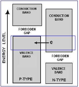
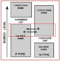
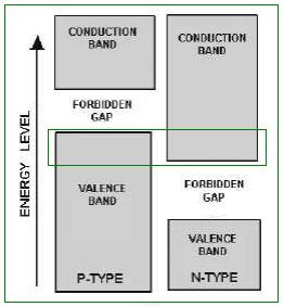
12 Operation
13 Tunnel Diode Forward Bias Operation -Tunnel diodes have a heavily doped p-n junction approximately 10 nm (100 A ) wide which results in overlap between energy bands. - As voltage begins to increase, electrons at first tunnel through the very narrow p-n junction barrier causing current to increase. - As voltage increases further these states become more misaligned and the current drops this is called negative resistance, because current decreases with increasing voltage. - As voltage increases yet further, the diode begins to operate as a normal diode, where electrons travel by conduction across the p-n junction, and no longer by tunneling through the p-n junction barrier.
14 Resonant Tunneling Tunneling is a quantum mechanical phenomenon with no analogy in classical physics. Occurs when an electron passes through a potential barrier without having enough energy to do so. Resonant tunneling can be described by the transmission and reflection processes of coherent electron waves through the double barrier structure. Can be seen as leaking of the amplitude through the potential step.


15 Tunneling Even though the transmission coefficient or the tunneling probability of an incident particle through the barrier is always less than one and decreases with increasing barrier height and width, two barriers in a row can be completely transparent for certain energies of the incident particle. This phenomenon is called resonant tunneling.
16 Tunneling Requirements Need good (high quality) heterostructures Quantum well layers Tunnel layers with high energy-barriers Requires junction to be abrupt Above, currently difficult on Si substrate
17 Heterostructures Heterostructures are structures with two or more interfaces at the boundaries between the regions of different materials. Compound semiconductors from Group (III V) are widely used to fabricate heterostructures. A double-barrier structure can be grown by molecular beam heteroepitaxy (MBE). Common compounds used are GaAs (gallium arsenide) and AlAs (aluminum arsenide) Band offsets at the boundary of heterojunction can depend on the quality of the interface, conditions of growth etc. Types I, II and broken-gap lineup heterojunctions
18 Type I The lowest conduction-band states occur in the same part of the structure as the highest valence-band states. (GaAs/Al x Ga 1-x As, is type I) Type II The lowest conduction-band minimum occurs on one side and the highest valence-band maximum on the other with an energy separation between the two is less than the lower of the two bulk bandgaps. (AlAs/Al x Ga 1-x As and some Si/Si x Ge 1-x structures) Broken-gap lineup The bottom of the conduction band on one side drops below the top of the valence band on the other. (InAs/GaSb gap of 150meV)


19 Molecular Beam Epitaxy Lab The most important aspect of MBE is the slow deposition rate, typically less than 1000 nm (1 micron) per hour, which allows the films to grow epitaxially.
20 Conduction band profiles of a double barrier RTD
21 RTD Challenges Scalability to below certain dimensions result in undesirable surface leakage current. Since the peak current through an RTD depends exponentially on the barrier thickness, it is difficult to get device operation unless the gate also controls the peak current. Integration of a transistor with a pair of RTDs introduces delays to the fast bistable switching times so, the operational speed of the integrated device can be slower than the intrinsic speeds of the RTDs themselves. The precise control of the layer thickness and properties of RTDs may require use of commercial molecular beam epitaxy to achieve the required control. A limited I ON /I OFF ratio of 10 compare to the ratio of 10 5 required by CMOS digital circuit designers. Fabrication of silicon or silicon-germanium tunnel diodes with high peak-to-valley current ratios.
22 Reasonably high performance III-V RTDs have been realized. But such devices have not entered mainstream applications yet because the processing of III-V materials is incompatible with Si CMOS technology. Although, RTD devices have several issues to overcome as described earlier, fabrication in a Si compatible material structure substantially reduces the integration challenges. Current research activity involving RTDs has been in the area of integration on the silicon platform.
.")
23 RTD on Si Substrates using Fluoride Alloy Heterostructures RTDs composed of CaF 2 -barrier/cdf 2 -well/ CaF 2 -barrier heterostructures are expected to be co-integrated with Si-Large Scale Integration (LSI). High speed LSI and low power consumption can be constructed in Siintegrated circuits.
24 Problems with compound fluoride structure Thickness of the CaF 2 barrier must be very thin to obtain enough current density due to excessive barrier height. Since chemical reactivity between Si and CdF 2 is very high, the CdF 2 well layer must be grown at very low temperature. This limits the overall growth temperature of the entire heterostructure. Results: poor yield of RTD and unstable electrical properties.

25 Solution Use Ca x Cd 1-x F 2 alloy for the overall structure and Cd-rich based alloy separation layers to protect the RTD active region. Cd-rich alloy can be grown with good crystallinity at higher temperature than for pure CdF 2 by adding a small amount of CaF 2 to CdF 2.
26 Solution The alloy Ca 0.5 Cd 0.5 F 2 showed the lower barrier height instead of CaF 2 and high PVCR. Similarly, RTDs using the Cd-rich alloy for the well exhibited even larger peak to valley current ratio at room temperature b/c of good crystallinity.

27 Result Ca 0.5 Cd 0.5 F 2 Ca 0.1 Cd 0.9 F 2
28 Applications OptoElectronic Integrated Circuits (OEICS) based on Group III-V RTDs can be used as oscillators, high frequency amplifiers, frequency converters and photodetectors. MOBILE circuits used in ultra high-speed analog to digital converters (80 Gb/s). MOBILE type structures can be applied to multi-valued threshold circuits and multi-threshold gates in general. Resonant-tunneling transistors - a negative transconductance that is used in logic XOR gate with only one transistor. Recent works also explore spin-polarized resonant tunneling, which can be useful for application in spintronic devices.
29 Integration of RTDs A pair of RTDs can be integrated with CMOS gate to achieve bi-stable operation. If connected in series with opposing polarities, results in MOBILE configuration. Trials of co-integration of the fluoride RTDs with Si-MOSFET have been reported. However, stability of electrical properties of the RTDs is insufficient (current drift) to realize circuit operations well at the moment. The origin is presumably charging effects of carrier traps in heterostructures. Further investigation to improve crystalline quality of the fluoride heterostructures is necessary to achieve reliable circuit operation of this device.
30 Devices
31 Conclusion Tunnel diodes are expected to add another node in the road Three-terminal tunnel devices could add several nodes at the end of CMOS-scaling Challenges are more practical than theoretical Uniformity of the tunneling barrier needs to be improved
32 References David Bohm, Quantum Theory, Prentice-Hall, New York, Baym Gordon, Lectures on Quantum Mechanics, Addison-Wesley Company, Canada, H. Mizuta and T. Tanoue. The Physics and applications of Resonant Tunnelling Diodes. Cambridge University Press, Cambridge Koichi Maezawa. Resonant Tunneling Diodes and Their Application to High-Speed Circuits. CSIC 2005 Digest, IEEE.
Introduction to Nanoelectronics. Topic Resonant Tunnel Diode. Professor R. Krchnavek. By Kalpesh Raval
 1 Introduction to Nanoelectronics Topic Resonant Tunnel Diode Professor R. Krchnavek By Kalpesh Raval 2 Over the several decades, the world of electronics has been dominated by Si (Silicon) based technologies.
Zaid abdul zahra hassan. Dept.of physics-collage of education for pure sciences. Babylon university
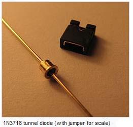
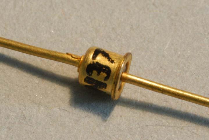
 Tunnel diode: Zaid abdul zahra hassan Dept.of physics-collage of education for pure sciences Babylon university 1N3716 tunnel diode (with jumper for scale) A tunnel diode or Esaki diode is a type of semiconductor
Chapter 1. Introduction
 Chapter 1 Introduction 1.1 Introduction of Device Technology Digital wireless communication system has become more and more popular in recent years due to its capability for both voice and data communication.
Downloaded from
 SOLID AND SEMICONDUCTOR DEVICES (EASY AND SCORING TOPIC) 1. Distinction of metals, semiconductor and insulator on the basis of Energy band of Solids. 2. Types of Semiconductor. 3. PN Junction formation
Electronic devices-i. Difference between conductors, insulators and semiconductors
 Electronic devices-i Semiconductor Devices is one of the important and easy units in class XII CBSE Physics syllabus. It is easy to understand and learn. Generally the questions asked are simple. The unit
Chapter Semiconductor Electronics
 Chapter Semiconductor Electronics Q1. p-n junction is said to be forward biased, when [1988] (a) the positive pole of the battery is joined to the p- semiconductor and negative pole to the n- semiconductor
Optoelectronic integrated circuits incorporating negative differential resistance devices
 Optoelectronic integrated circuits incorporating negative differential resistance devices José Figueiredo Centro de Electrónica, Optoelectrónica e Telecomunicações Departamento de Física da Faculdade de
Electronic Circuits I. Instructor: Dr. Alaa Mahmoud
 Electronic Circuits I Instructor: Dr. Alaa Mahmoud alaa_y_emam@hotmail.com Chapter 27 Diode and diode application Outline: Semiconductor Materials The P-N Junction Diode Biasing P-N Junction Volt-Ampere
Ultra-low voltage resonant tunnelling diode electroabsorption modulator
 Ultra-low voltage resonant tunnelling diode electroabsorption modulator, 1/10 Ultra-low voltage resonant tunnelling diode electroabsorption modulator J. M. L. FIGUEIREDO Faculdade de Ciências e Tecnologia,
Semiconductor Physics and Devices
 Metal-Semiconductor and Semiconductor Heterojunctions The Metal-Oxide-Semiconductor Field-Effect Transistor (MOSFET) is one of two major types of transistors. The MOSFET is used in digital circuit, because
15 Transit Time and Tunnel NDR Devices
 15 Transit Time and Tunnel NDR Devices Schematics of Transit-time NDR diode. A packet of carriers (e.g., electrons) is generated in a confined and narrow zone (generation region) and injected into the
Prepared by: Dr. Rishi Prakash, Dept of Electronics and Communication Engineering Page 1 of 5
 Microwave tunnel diode Some anomalous phenomena were observed in diode which do not follows the classical diode equation. This anomalous phenomena was explained by quantum tunnelling theory. The tunnelling
NAME: Last First Signature
 UNIVERSITY OF CALIFORNIA, BERKELEY College of Engineering Department of Electrical Engineering and Computer Sciences EE 130: IC Devices Spring 2003 FINAL EXAMINATION NAME: Last First Signature STUDENT
1- Light Emitting Diode (LED)
") Content: - Special Purpose two terminal Devices: Light-Emitting Diodes, Varactor (Varicap)Diodes, Tunnel Diodes, Liquid-Crystal Displays. 1- Light Emitting Diode (LED) Light Emitting Diode is a photo electronic
Content: - Special Purpose two terminal Devices: Light-Emitting Diodes, Varactor (Varicap)Diodes, Tunnel Diodes, Liquid-Crystal Displays. 1- Light Emitting Diode (LED) Light Emitting Diode is a photo electronic
Title. Author(s)Uemura, T.; Baba, T. CitationIEEE Transactions on Electron Devices, 49(8): Issue Date Doc URL. Rights.
Uemura, T.; Baba, T. CitationIEEE Transactions on Electron Devices, 49(8): Issue Date Doc URL. Rights.") Title A three-valued D-flip-flop and shift register using Author(s)Uemura, T.; Baba, T. CitationIEEE Transactions on Electron Devices, 49(8): 1336-1 Issue Date 2002-08 Doc URL http://hdl.handle.net/2115/5577
Title A three-valued D-flip-flop and shift register using Author(s)Uemura, T.; Baba, T. CitationIEEE Transactions on Electron Devices, 49(8): 1336-1 Issue Date 2002-08 Doc URL http://hdl.handle.net/2115/5577
 Electronic Devices 1. Current flowing in each of the following circuits A and respectively are: (Circuit 1) (Circuit 2) 1) 1A, 2A 2) 2A, 1A 3) 4A, 2A 4) 2A, 4A 2. Among the following one statement is not
Review Energy Bands Carrier Density & Mobility Carrier Transport Generation and Recombination
 Review Energy Bands Carrier Density & Mobility Carrier Transport Generation and Recombination Current Transport: Diffusion, Thermionic Emission & Tunneling For Diffusion current, the depletion layer is
Università degli Studi di Roma Tor Vergata Dipartimento di Ingegneria Elettronica. Analogue Electronics. Paolo Colantonio A.A.
 Università degli Studi di Roma Tor Vergata Dipartimento di Ingegneria Elettronica Analogue Electronics Paolo Colantonio A.A. 2015-16 Introduction: materials Conductors e.g. copper or aluminum have a cloud
420 Intro to VLSI Design
 Dept of Electrical and Computer Engineering 420 Intro to VLSI Design Lecture 0: Course Introduction and Overview Valencia M. Joyner Spring 2005 Getting Started Syllabus About the Instructor Labs, Problem
SRM INSTITUTE OF SCIENCE AND TECHNOLOGY (DEEMED UNIVERSITY)
") SRM INSTITUTE OF SCIENCE AND TECHNOLOGY (DEEMED UNIVERSITY) QUESTION BANK I YEAR B.Tech (II Semester) ELECTRONIC DEVICES (COMMON FOR EC102, EE104, IC108, BM106) UNIT-I PART-A 1. What are intrinsic and
SRM INSTITUTE OF SCIENCE AND TECHNOLOGY (DEEMED UNIVERSITY) QUESTION BANK I YEAR B.Tech (II Semester) ELECTRONIC DEVICES (COMMON FOR EC102, EE104, IC108, BM106) UNIT-I PART-A 1. What are intrinsic and
Intro to Electricity. Introduction to Transistors. Example Circuit Diagrams. Water Analogy
 Introduction to Transistors Transistors form the basic building blocks of all computer hardware. Invented by William Shockley, John Bardeen and Walter Brattain in 1947, replacing previous vaccuumtube technology
UNIT IX ELECTRONIC DEVICES
 UNT X ELECTRONC DECES Weightage Marks : 07 Semiconductors Semiconductors diode-- characteristics in forward and reverse bias, diode as rectifier. - characteristics of LED, Photodiodes, solarcell and Zener
Power Semiconductor Devices
 TRADEMARK OF INNOVATION Power Semiconductor Devices Introduction This technical article is dedicated to the review of the following power electronics devices which act as solid-state switches in the circuits.
Chapter 1: Semiconductor Diodes
 Chapter 1: Semiconductor Diodes Diodes The diode is a 2-terminal device. A diode ideally conducts in only one direction. 2 Diode Characteristics Conduction Region Non-Conduction Region The voltage across
UNIT-4. Microwave Engineering
 UNIT-4 Microwave Engineering Microwave Solid State Devices Two problems with conventional transistors at higher frequencies are: 1. Stray capacitance and inductance. - remedy is interdigital design. 2.Transit
PHYS 3050 Electronics I
 PHYS 3050 Electronics I Chapter 4. Semiconductor Diodes and Transistors Earth, Moon, Mars, and Beyond Dr. Jinjun Shan, Associate Professor of Space Engineering Department of Earth and Space Science and
Lesson 08. Name and affiliation of the author: Professor L B D R P Wijesundera Department of Physics, University of Kelaniya.
 Lesson 08 Title of the Experiment: Identification of active components in electronic circuits and characteristics of a Diode, Zener diode and LED (Activity number of the GCE Advanced Level practical Guide
MSE 410/ECE 340: Electrical Properties of Materials Fall 2016 Micron School of Materials Science and Engineering Boise State University
 MSE 410/ECE 340: Electrical Properties of Materials Fall 2016 Micron School of Materials Science and Engineering Boise State University Practice Final Exam 1 Read the questions carefully Label all figures
Digital Electronics. By: FARHAD FARADJI, Ph.D. Assistant Professor, Electrical and Computer Engineering, K. N. Toosi University of Technology
 K. N. Toosi University of Technology Chapter 7. Field-Effect Transistors By: FARHAD FARADJI, Ph.D. Assistant Professor, Electrical and Computer Engineering, K. N. Toosi University of Technology http://wp.kntu.ac.ir/faradji/digitalelectronics.htm
Optodevice Data Book ODE I. Rev.9 Mar Opnext Japan, Inc.
 Optodevice Data Book ODE-408-001I Rev.9 Mar. 2003 Opnext Japan, Inc. Section 1 Operating Principles 1.1 Operating Principles of Laser Diodes (LDs) and Infrared Emitting Diodes (IREDs) 1.1.1 Emitting Principles
Electron Devices and Circuits (EC 8353)
") Electron Devices and Circuits (EC 8353) Prepared by Ms.S.KARKUZHALI, A.P/EEE Diodes The diode is a 2-terminal device. A diode ideally conducts in only one direction. Diode Characteristics Conduction Region
Electron Devices and Circuits (EC 8353) Prepared by Ms.S.KARKUZHALI, A.P/EEE Diodes The diode is a 2-terminal device. A diode ideally conducts in only one direction. Diode Characteristics Conduction Region
Module 04.(B1) Electronic Fundamentals
 Electronic Fundamentals") 1.1a. Semiconductors - Diodes. Module 04.(B1) Electronic Fundamentals Question Number. 1. What gives the colour of an LED?. Option A. The active element. Option B. The plastic it is encased in. Option
1.1a. Semiconductors - Diodes. Module 04.(B1) Electronic Fundamentals Question Number. 1. What gives the colour of an LED?. Option A. The active element. Option B. The plastic it is encased in. Option
LEDs, Photodetectors and Solar Cells
 LEDs, Photodetectors and Solar Cells Chapter 7 (Parker) ELEC 424 John Peeples Why the Interest in Photons? Answer: Momentum and Radiation High electrical current density destroys minute polysilicon and
UNIT-VI FIELD EFFECT TRANSISTOR. 1. Explain about the Field Effect Transistor and also mention types of FET s.
 UNIT-I FIELD EFFECT TRANSISTOR 1. Explain about the Field Effect Transistor and also mention types of FET s. The Field Effect Transistor, or simply FET however, uses the voltage that is applied to their
Innovative ultra-broadband ubiquitous Wireless communications through terahertz transceivers ibrow
 Project Overview Innovative ultra-broadband ubiquitous Wireless communications through terahertz transceivers ibrow Mar-2017 Presentation outline Project key facts Motivation Project objectives Project
Tunneling Field Effect Transistors for Low Power ULSI
 Tunneling Field Effect Transistors for Low Power ULSI Byung-Gook Park Inter-university Semiconductor Research Center and School of Electrical and Computer Engineering Seoul National University Outline
CONTENTS. 2.2 Schrodinger's Wave Equation 31. PART I Semiconductor Material Properties. 2.3 Applications of Schrodinger's Wave Equation 34
 CONTENTS Preface x Prologue Semiconductors and the Integrated Circuit xvii PART I Semiconductor Material Properties CHAPTER 1 The Crystal Structure of Solids 1 1.0 Preview 1 1.1 Semiconductor Materials
EE 5611 Introduction to Microelectronic Technologies Fall Thursday, September 04, 2014 Lecture 02
 EE 5611 Introduction to Microelectronic Technologies Fall 2014 Thursday, September 04, 2014 Lecture 02 1 Lecture Outline Review on semiconductor materials Review on microelectronic devices Example of microelectronic
value of W max for the device. The at band voltage is -0.9 V. Problem 5: An Al-gate n-channel MOS capacitor has a doping of N a = cm ;3. The oxi
 Prof. Jasprit Singh Fall 2001 EECS 320 Homework 10 This homework is due on December 6 Problem 1: An n-type In 0:53 Ga 0:47 As epitaxial layer doped at 10 16 cm ;3 is to be used as a channel in a FET. A
Quantum Condensed Matter Physics Lecture 16
 Quantum Condensed Matter Physics Lecture 16 David Ritchie QCMP Lent/Easter 2018 http://www.sp.phy.cam.ac.uk/drp2/home 16.1 Quantum Condensed Matter Physics 1. Classical and Semi-classical models for electrons
Lecture 18: Photodetectors
 Lecture 18: Photodetectors Contents 1 Introduction 1 2 Photodetector principle 2 3 Photoconductor 4 4 Photodiodes 6 4.1 Heterojunction photodiode.................... 8 4.2 Metal-semiconductor photodiode................
UNIT 3 Transistors JFET
 UNIT 3 Transistors JFET Mosfet Definition of BJT A bipolar junction transistor is a three terminal semiconductor device consisting of two p-n junctions which is able to amplify or magnify a signal. It
Downloaded from
 Question 14.1: In an n-type silicon, which of the following statement is true: (a) Electrons are majority carriers and trivalent atoms are the dopants. (b) Electrons are minority carriers and pentavalent
The resonant tunneling diode-laser diode optoelectronic integrated circuit operating as a voltage controlled oscillator
 The resonant tunneling diode-laser diode optoelectronic integrated circuit operating as a voltage controlled oscillator C. N. Ironside a, T. J. Slight a, L. Wang a and E. Wasige a, B. Romeira b and J.
THERMIONIC AND GASEOUS STATE DIODES
 THERMIONIC AND GASEOUS STATE DIODES Thermionic and gaseous state (vacuum tube) diodes Thermionic diodes are thermionic-valve devices (also known as vacuum tubes, tubes, or valves), which are arrangements
SEMICONDUCTOR ELECTRONICS: MATERIALS, DEVICES AND SIMPLE CIRCUITS. Class XII : PHYSICS WORKSHEET
 SEMICONDUCT ELECTRONICS: MATERIALS, DEVICES AND SIMPLE CIRCUITS Class XII : PHYSICS WKSHEET 1. How is a n-p-n transistor represented symbolically? (1) 2. How does conductivity of a semiconductor change
A Brief Introduction to Single Electron Transistors. December 18, 2011
 A Brief Introduction to Single Electron Transistors Diogo AGUIAM OBRECZÁN Vince December 18, 2011 1 Abstract Transistor integration has come a long way since Moore s Law was first mentioned and current
Alternatives to standard MOSFETs. What problems are we really trying to solve?
 Alternatives to standard MOSFETs A number of alternative FET schemes have been proposed, with an eye toward scaling up to the 10 nm node. Modifications to the standard MOSFET include: Silicon-in-insulator
Student Lecture by: Giangiacomo Groppi Joel Cassell Pierre Berthelot September 28 th 2004
 Student Lecture by: Giangiacomo Groppi Joel Cassell Pierre Berthelot September 28 th 2004 Lecture outline Historical introduction Semiconductor devices overview Bipolar Junction Transistor (BJT) Field
Lecture 2 p-n junction Diode characteristics. By Asst. Prof Dr. Jassim K. Hmood
 Electronic I Lecture 2 p-n junction Diode characteristics By Asst. Prof Dr. Jassim K. Hmood THE p-n JUNCTION DIODE The pn junction diode is formed by fabrication of a p-type semiconductor region in intimate
Semiconductor Physics and Devices
 Nonideal Effect The experimental characteristics of MOSFETs deviate to some degree from the ideal relations that have been theoretically derived. Semiconductor Physics and Devices Chapter 11. MOSFET: Additional
Department of Electrical Engineering IIT Madras
 Department of Electrical Engineering IIT Madras Sample Questions on Semiconductor Devices EE3 applicants who are interested to pursue their research in microelectronics devices area (fabrication and/or
General look back at MESFET processing. General principles of heterostructure use in FETs
 SMA5111 - Compound Semiconductors Lecture 11 - Heterojunction FETs - General HJFETs, HFETs Last items from Lec. 10 Depletion mode vs enhancement mode logic Complementary FET logic (none exists, or is likely
In this lecture we will begin a new topic namely the Metal-Oxide-Semiconductor Field Effect Transistor.
 Solid State Devices Dr. S. Karmalkar Department of Electronics and Communication Engineering Indian Institute of Technology, Madras Lecture - 38 MOS Field Effect Transistor In this lecture we will begin
UNIT VIII-SPECIAL PURPOSE ELECTRONIC DEVICES. 1. Explain tunnel Diode operation with the help of energy band diagrams.
 UNIT III-SPECIAL PURPOSE ELECTRONIC DEICES 1. Explain tunnel Diode operation with the help of energy band diagrams. TUNNEL DIODE: A tunnel diode or Esaki diode is a type of semiconductor diode which is
Comparative Study of Silicon and Germanium Doping-less Tunnel Field Effect Transistors
 IJSTE - International Journal of Science Technology & Engineering Volume 2 Issue 5 November 2015 ISSN (online): 2349-784X Comparative Study of Silicon and Germanium Doping-less Tunnel Field Effect Transistors
INTERNATIONAL JOURNAL OF APPLIED ENGINEERING RESEARCH, DINDIGUL Volume 1, No 3, 2010
 Low Power CMOS Inverter design at different Technologies Vijay Kumar Sharma 1, Surender Soni 2 1 Department of Electronics & Communication, College of Engineering, Teerthanker Mahaveer University, Moradabad
Lecture - 19 Microwave Solid State Diode Oscillator and Amplifier
 Basic Building Blocks of Microwave Engineering Prof. Amitabha Bhattacharya Department of Electronics and Communication Engineering Indian Institute of Technology, Kharagpur Lecture - 19 Microwave Solid
Solid State Devices- Part- II. Module- IV
 Solid State Devices- Part- II Module- IV MOS Capacitor Two terminal MOS device MOS = Metal- Oxide- Semiconductor MOS capacitor - the heart of the MOSFET The MOS capacitor is used to induce charge at the
Gallium nitride (GaN)
") 80 Technology focus: GaN power electronics Vertical, CMOS and dual-gate approaches to gallium nitride power electronics US research company HRL Laboratories has published a number of papers concerning
80 Technology focus: GaN power electronics Vertical, CMOS and dual-gate approaches to gallium nitride power electronics US research company HRL Laboratories has published a number of papers concerning
ECE 340 Lecture 29 : LEDs and Lasers Class Outline:
 ECE 340 Lecture 29 : LEDs and Lasers Class Outline: Light Emitting Diodes Lasers Semiconductor Lasers Things you should know when you leave Key Questions What is an LED and how does it work? How does a
Key Questions. What is an LED and how does it work? How does a laser work? How does a semiconductor laser work? ECE 340 Lecture 29 : LEDs and Lasers
 Things you should know when you leave Key Questions ECE 340 Lecture 29 : LEDs and Class Outline: What is an LED and how does it How does a laser How does a semiconductor laser How do light emitting diodes
Chapter 3: Basics Semiconductor Devices and Processing 2006/9/27 1. Topics
 Chapter 3: Basics Semiconductor Devices and Processing 2006/9/27 1 Topics What is semiconductor Basic semiconductor devices Basics of IC processing CMOS technologies 2006/9/27 2 1 What is Semiconductor
Avalanche Photodiode. Instructor: Prof. Dietmar Knipp Presentation by Peter Egyinam. 4/19/2005 Photonics and Optical communicaton
 Avalanche Photodiode Instructor: Prof. Dietmar Knipp Presentation by Peter Egyinam 1 Outline Background of Photodiodes General Purpose of Photodiodes Basic operation of p-n, p-i-n and avalanche photodiodes
1) A silicon diode measures a low value of resistance with the meter leads in both positions. The trouble, if any, is
 A silicon diode measures a low value of resistance with the meter leads in both positions. The trouble, if any, is") 1) A silicon diode measures a low value of resistance with the meter leads in both positions. The trouble, if any, is A [ ]) the diode is open. B [ ]) the diode is shorted to ground. C [v]) the diode is
1) A silicon diode measures a low value of resistance with the meter leads in both positions. The trouble, if any, is A [ ]) the diode is open. B [ ]) the diode is shorted to ground. C [v]) the diode is
Lesson 5. Electronics: Semiconductors Doping p-n Junction Diode Half Wave and Full Wave Rectification Introduction to Transistors-
 Lesson 5 Electronics: Semiconductors Doping p-n Junction Diode Half Wave and Full Wave Rectification Introduction to Transistors- Types and Connections Semiconductors Semiconductors If there are many free
Chapter 6. Silicon-Germanium Technologies
 Chapter 6 licon-germanium Technologies 6.0 Introduction The design of bipolar transistors requires trade-offs between a number of parameters. To achieve a fast base transit time, hence achieving a high
Lecture: Integration of silicon photonics with electronics. Prepared by Jean-Marc FEDELI CEA-LETI
 Lecture: Integration of silicon photonics with electronics Prepared by Jean-Marc FEDELI CEA-LETI Context The goal is to give optical functionalities to electronics integrated circuit (EIC) The objectives
Numerical Analysis of Triple Barrier GaAs/ Al x Ga 1-x As Resonant Tunneling Structure Using PMM Approach
 266 Numerical Analysis of Triple Barrier GaAs/ Al x Ga 1-x As Resonant Tunneling Structure Using PMM Approach Abbas Zarifkar, Abolfazl Mohammadi Bagherabadi Iran Telecommunication Research Center, Tehran,
Power MOSFET Zheng Yang (ERF 3017,
 ECE442 Power Semiconductor Devices and Integrated Circuits Power MOSFET Zheng Yang (ERF 3017, email: yangzhen@uic.edu) Evolution of low-voltage (
Optical Fiber Communication Lecture 11 Detectors
 Optical Fiber Communication Lecture 11 Detectors Warriors of the Net Detector Technologies MSM (Metal Semiconductor Metal) PIN Layer Structure Semiinsulating GaAs Contact InGaAsP p 5x10 18 Absorption InGaAs
CHAPTER FORMULAS & NOTES
 Formulae For u SEMICONDUCTORS By Mir Mohammed Abbas II PCMB 'A' 1 Important Terms, Definitions & Formulae CHAPTER FORMULAS & NOTES 1 Intrinsic Semiconductor: The pure semiconductors in which the electrical
Transistor was first invented by William.B.Shockley, Walter Brattain and John Bardeen of Bell Labratories. In 1961, first IC was introduced.
 Unit 1 Basic MOS Technology Transistor was first invented by William.B.Shockley, Walter Brattain and John Bardeen of Bell Labratories. In 1961, first IC was introduced. Levels of Integration:- i) SSI:-
Semiconductor Memory: DRAM and SRAM. Department of Electrical and Computer Engineering, National University of Singapore
 Semiconductor Memory: DRAM and SRAM Outline Introduction Random Access Memory (RAM) DRAM SRAM Non-volatile memory UV EPROM EEPROM Flash memory SONOS memory QD memory Introduction Slow memories Magnetic
Difference between BJTs and FETs. Junction Field Effect Transistors (JFET)
") Difference between BJTs and FETs Transistors can be categorized according to their structure, and two of the more commonly known transistor structures, are the BJT and FET. The comparison between BJTs
Difference between BJTs and FETs Transistors can be categorized according to their structure, and two of the more commonly known transistor structures, are the BJT and FET. The comparison between BJTs
Lecture 7:PN Junction. Structure, Depletion region, Different bias Conditions, IV characteristics, Examples
 Lecture 7:PN Junction Structure, Depletion region, Different bias Conditions, IV characteristics, Examples PN Junction The diode (pn junction) is formed by dopping a piece of intrinsic silicon, such that
Electronics The basics of semiconductor physics
 Electronics The basics of semiconductor physics Prof. Márta Rencz, Gábor Takács BME DED 17/09/2015 1 / 37 The basic properties of semiconductors Range of conductivity [Source: http://www.britannica.com]
Photodynamics Research Center, The Institute of Physical and Chemical Research, Aza-Koeji, Nagamachi, Aoba-ku, Sendai 980, Japan
 SERIES CONNECTION OF RESONANT TUNNELING DIODES FOR ELIMINATING SPURIOUS OSCILLATIONS Tetsu Fujii 1,2, Olga Boric-Lubecke l, Jongsuck Bae 1.2, and Koji Mizuno 1.2 Photodynamics Research Center, The Institute
Design and Analysis of Double Gate MOSFET Devices using High-k Dielectric
 International Journal of Electrical Engineering. ISSN 0974-2158 Volume 7, Number 1 (2014), pp. 53-60 International Research Publication House http://www.irphouse.com Design and Analysis of Double Gate
Semiconductor Lasers Semiconductors were originally pumped by lasers or e-beams First diode types developed in 1962: Create a pn junction in
 Semiconductor Lasers Semiconductors were originally pumped by lasers or e-beams First diode types developed in 1962: Create a pn junction in semiconductor material Pumped now with high current density
What is the highest efficiency Solar Cell?
 What is the highest efficiency Solar Cell? GT CRC Roof-Mounted PV System Largest single PV structure at the time of it s construction for the 1996 Olympic games Produced more than 1 billion watt hrs. of
Physics of Waveguide Photodetectors with Integrated Amplification
 Physics of Waveguide Photodetectors with Integrated Amplification J. Piprek, D. Lasaosa, D. Pasquariello, and J. E. Bowers Electrical and Computer Engineering Department University of California, Santa
IENGINEERS- CONSULTANTS LECTURE NOTES SERIES ELECTRONICS ENGINEERING 1 YEAR UPTU. Lecture-4
 2 P-n Lecture-4 20 Introduction: If a junction is formed between a p-type and a n-type semiconductor this combination is known as p-n junction diode and has the properties of a rectifier 21 Formation of
Performance Evaluation of MISISFET- TCAD Simulation
 Performance Evaluation of MISISFET- TCAD Simulation Tarun Chaudhary Gargi Khanna Rajeevan Chandel ABSTRACT A novel device n-misisfet with a dielectric stack instead of the single insulator of n-mosfet
EECE251 Circuit Analysis I Set 6: Diodes
 EECE251 Circuit Analysis I Set 6: Diodes Shahriar Mirabbasi Department of Electrical and Computer Engineering University of British Columbia shahriar@ece.ubc.ca Thanks to Dr. Linares and Dr. Yan for sharing
Simulation of GaAs MESFET and HEMT Devices for RF Applications
 olume, Issue, January February 03 ISSN 78-6856 Simulation of GaAs MESFET and HEMT Devices for RF Applications Dr.E.N.GANESH Prof, ECE DEPT. Rajalakshmi Institute of Technology ABSTRACT: Field effect transistor
LSI ON GLASS SUBSTRATES
 LSI ON GLASS SUBSTRATES OUTLINE Introduction: Why System on Glass? MOSFET Technology Low-Temperature Poly-Si TFT Technology System-on-Glass Technology Issues Conclusion System on Glass CPU SRAM DRAM EEPROM
Intrinsic Semiconductor
 Semiconductors Crystalline solid materials whose resistivities are values between those of conductors and insulators. Good electrical characteristics and feasible fabrication technology are some reasons
Diode conducts when V anode > V cathode. Positive current flow. Diodes (and transistors) are non-linear device: V IR!
 are non-linear device: V IR!") Diodes: What do we use diodes for? Lecture 5: Diodes and Transistors protect circuits by limiting the voltage (clipping and clamping) turn AC into DC (voltage rectifier) voltage multipliers (e.g. double
Diodes: What do we use diodes for? Lecture 5: Diodes and Transistors protect circuits by limiting the voltage (clipping and clamping) turn AC into DC (voltage rectifier) voltage multipliers (e.g. double
Power Bipolar Junction Transistors (BJTs)
") ECE442 Power Semiconductor Devices and Integrated Circuits Power Bipolar Junction Transistors (BJTs) Zheng Yang (ERF 3017, email: yangzhen@uic.edu) Power Bipolar Junction Transistor (BJT) Background The
ECE442 Power Semiconductor Devices and Integrated Circuits Power Bipolar Junction Transistors (BJTs) Zheng Yang (ERF 3017, email: yangzhen@uic.edu) Power Bipolar Junction Transistor (BJT) Background The
Fundamentals of Power Semiconductor Devices
 В. Jayant Baliga Fundamentals of Power Semiconductor Devices 4y Spri ringer Contents Preface vii Chapter 1 Introduction 1 1.1 Ideal and Typical Power Switching Waveforms 3 1.2 Ideal and Typical Power Device
PN Junction in equilibrium
 PN Junction in equilibrium PN junctions are important for the following reasons: (i) PN junction is an important semiconductor device in itself and used in a wide variety of applications such as rectifiers,
Physics 160 Lecture 5. R. Johnson April 13, 2015
 Physics 160 Lecture 5 R. Johnson April 13, 2015 Half Wave Diode Rectifiers Full Wave April 13, 2015 Physics 160 2 Note that there is no ground connection on this side of the rectifier! Output Smoothing
INTRODUCTION: Basic operating principle of a MOSFET:
 INTRODUCTION: Along with the Junction Field Effect Transistor (JFET), there is another type of Field Effect Transistor available whose Gate input is electrically insulated from the main current carrying
Semiconductor Lasers Semiconductors were originally pumped by lasers or e-beams First diode types developed in 1962: Create a pn junction in
 Semiconductor Lasers Semiconductors were originally pumped by lasers or e-beams First diode types developed in 1962: Create a pn junction in semiconductor material Pumped now with high current density
CHAPTER 8 The PN Junction Diode
 CHAPTER 8 The PN Junction Diode Consider the process by which the potential barrier of a PN junction is lowered when a forward bias voltage is applied, so holes and electrons can flow across the junction
Discuss the basic structure of atoms Discuss properties of insulators, conductors, and semiconductors
 Discuss the basic structure of atoms Discuss properties of insulators, conductors, and semiconductors Discuss covalent bonding Describe the properties of both p and n type materials Discuss both forward
Module IV, Lecture 2 DNP experiments and hardware
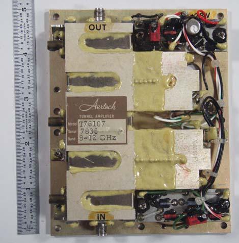
 Module IV, Lecture 2 DNP experiments and hardware tunnel diodes, Gunn diodes, magnetrons, traveling-wave tubes, klystrons, gyrotrons Dr Ilya Kuprov, University of Southampton, 2013 (for all lecture notes
InP-based Waveguide Photodetector with Integrated Photon Multiplication
 InP-based Waveguide Photodetector with Integrated Photon Multiplication D.Pasquariello,J.Piprek,D.Lasaosa,andJ.E.Bowers Electrical and Computer Engineering Department University of California, Santa Barbara,
 Energy band diagrams Metals: 9. ELECTRONIC DEVICES GIST ρ= 10-2 to 10-8 Ω m Insulators: ρ> 10 8 Ω m Semiconductors ρ= 1 to 10 5 Ω m 109 A. Intrinsic semiconductors At T=0k it acts as insulator At room